

Page 1
XR-MK7
HC, HR
SERVICE MANUAL
COMPACT DISC STEREO
SYSTEM
This Service Manual is the "Revision Publishing" and replaces "Simple Manual"
(S/M Code No. 09-99B-337-9T1).
SPECIFICATIONS
BASIC CD MECHANISM : DA11T3C
Design and specifications are subject to change without
•
notice
.
S/M Code No. 09-001-337-9R1
REVISION
DATA
Page 2

TABLE OF CONTENTS
PROTECTION OF EYES FROM LASER BEAM DURING SERVICING/
Precaution to replace Optical block......................................................................................................... 3
ELECTRICAL MAIN PARTS LIST ....................................................................................................... 4-8
TRANSISTOR ILLUSTRATION .............................................................................................................. 8
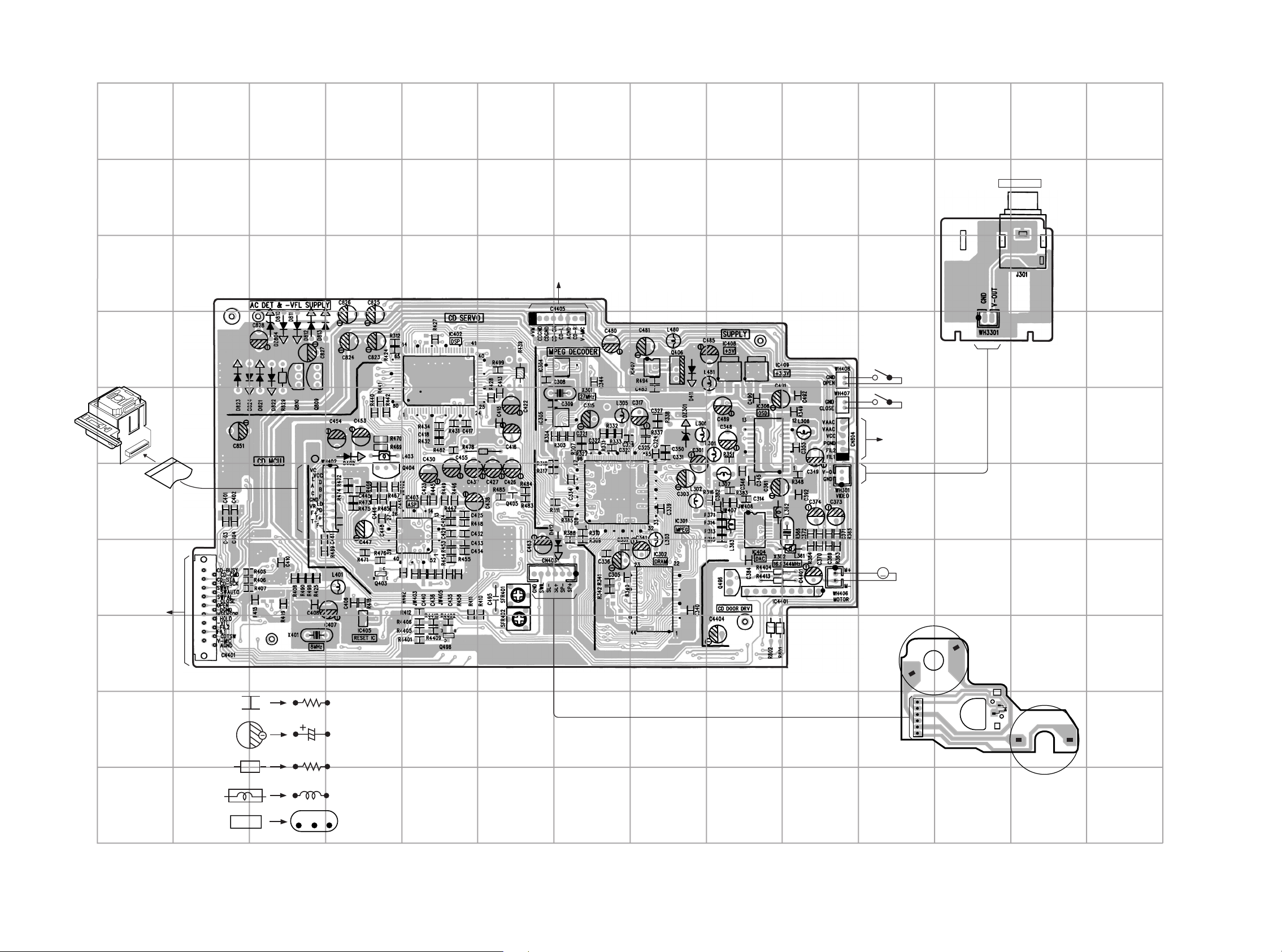
BLOCK DIAGRAM-1 (CD/CONTROL).............................................................................................. 9, 10
BLOCK DIAGRAM-2 (POWER/AMP) ............................................................................................. 11, 12
BLOCK DIAGRAM-3 (VIDEO/DISPLAY) ........................................................................................ 13, 14
WIRING-1 (MAIN: COMPONENT SIDE) ........................................................................................ 15, 16
WIRING-2 (MAIN: CONDUCTOR SIDE) ........................................................................................ 17, 18
SCHEMATIC DIAGRAM-1 (MAIN).................................................................................................. 19, 20
SCHEMATIC DIAGRAM-2 (VCD 1/3) ............................................................................................. 21, 22
SCHEMATIC DIAGRAM-3 (VCD 2/3) ............................................................................................. 23, 24
SCHEMATIC DIAGRAM-4 (VCD 3/3) ............................................................................................. 25, 26
WIRING-3 (VCD: COMPONENT SIDE).......................................................................................... 27, 28
WIRING-4 (VCD: CONDUCTOR SIDE).......................................................................................... 29, 30
WIRING-5 (TUNER)........................................................................................................................ 31, 32
SCHEMATIC DIAGRAM-5 (TUNER) .............................................................................................. 33, 34
WIRING-6 (DISPLAY: COMPONENT SIDE) .................................................................................. 35, 36
WIRING-7 (DISPLAY: CONDUCTOR SIDE) .................................................................................. 37, 38
SCHEMATIC DIAGRAM-6 (DISPLAY) ........................................................................................... 39, 40
WIRING-8 (PT)................................................................................................................................ 41, 42
SCHEMATIC DIAGRAM-7 (PT) ...................................................................................................... 43, 44
VOLTAGE CHART........................................................................................................................... 45-50
FL GRID ASSIGNMENT/ANODE CONNECTION .......................................................................... 51, 52
ELECTRICAL ADJUSTMENT/PRACTICAL SERVICE FIGURE .................................................... 53, 54
IC DESCRIPTION............................................................................................................................ 55-68
IC BLOCK DIAGRAM....................................................................................................................... 69-74
MECHANICAL EXPLODED VIEW 1/1............................................................................................ 75, 76
MECHANICAL PARTS LIST 1/1 ........................................................................................................... 77
CD MECHANISM EXPLODED VIEW 1/1 ............................................................................................. 78
CD MECHANISM PARTS LIST 1/1 ...................................................................................................... 78
SPEAKER DISASSEMBLY INSTRUCTIONS....................................................................................... 79
SPEAKER PARTS LIST 1/1.................................................................................................................. 80
ACCESSORIES/PACKAGE LIST ......................................................................................................... 81
2
Page 3
PROTECTION OF EYES FROM LASER BEAM DURING SERVICING
CLASS 1
KLASSE 1
LUOKAN 1
KLASS 1
LASER PRODUCT
LASER PRODUKT
LASER LAITE
LASER APPARAT
This set employs laser. Therefore, be sure to follow carefully the
instructions below when servicing.
WARNING!
WHEN SERVICING, DO NOT APPROACH THE LASER EXIT
WITH THE EYE TOO CLOSELY. IN CASE IT IS NECESSARY TO
CONFIRM LASER BEAM EMISSION. BE SURE TO OBSERVE
FROM A DISTANCE OF MORE THAN 30cm FROM THE
SURFACE OF THE OBJECTIVE LENS ON THE OPTICAL
PICK-UP BLOCK.
Caution: Invisible laser radiation when
open and interlocks defeated avoid exposure to beam.
Advarsel:Usynling laserståling ved åbning,
når sikkerhedsafbrydere er ude af funktion.
Undgå udsættelse for stråling.
VAROITUS!
Laiteen Käyttäminen muulla kuin tässä käyttöohjeessa mainitulla tavalla saattaa altistaa käyt-täjän turvallisuusluokan 1 ylittävälle näkymättömälle lasersäteilylle.
CAUTION
Use of controls or adjustments or performance of procedures
other than those specified herein may result in hazardous
radiation exposure.
ATTENTION
L'utilisation de commandes, réglages ou procédures autres que
ceux spécifiés peut entraîner une dangereuse exposition aux
radiations.
ADVARSEL!
Usynlig laserståling ved åbning, når sikkerhedsafbrydereer ude
af funktion. Undgå udsættelse for stråling.
This Compact Disc player is classified as a CLASS 1 LASER
product.
The CLASS 1 LASER PRODUCT label is located on the rear
exterior.
VARNING!
Om apparaten används på annat sätt än vad som specificeras i
denna bruksanvising, kan användaren utsättas för osynling
laserstrålning, som överskrider gränsen för laserklass 1.
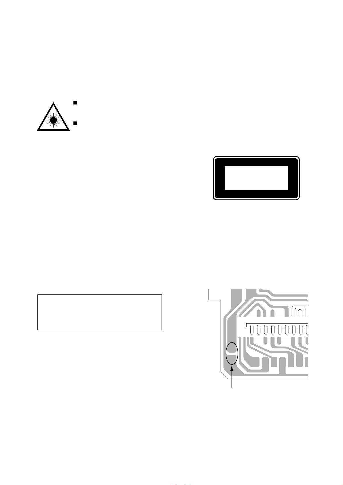
Precaution to replace Optical block
(SF-P101NR)
Body or clothes electrostatic potential could ruin
laser diode in the optical block. Be sure ground
body and workbench, and use care the clothes
do not touch the diode.
1) After the connection, remove solder shown in
the right figure.
PICK-UP Assy P.C.B
Solder
3
Page 4

ELECTRICAL MAIN PARTS LIST
REF. NO PART NO. KANRI DESCRIPTION
NO.
IC
8Z-CL5-641-010 C-IC,LC876572-5N64
87-070-282-010 IC,BU2092
8Z-CL5-616-010 IC,RPM638CBRL676/6938-V4
87-A20-920-010 C-IC,CL680-D1
87-A20-962-040 C-IC,MSM54V16258B/BSL
84-ZG1-695-040 C-IC,LH5V2RN1
87-A20-975-040 C-IC,SN74LV74APW
87-A20-921-040 C-IC,SN74LVU04APW
87-A20-974-040 C-IC,LC74781M-9017
8Z-CDW-615-010 C-IC,UPD78016FGC-570-AB8
87-A20-917-010 C-IC,CXD2540Q-1/2
87-A20-547-010 C-IC,CXA1992AR
87-A20-918-040 C-IC,SM5878AM
87-A20-592-040 C-IC,M51943 AML
87-A20-919-040 C-IC,BA5915FP
87-A20-602-040 C-IC,M5291FP
87-A20-925-040 C-IC,BA05FP
87-A20-905-040 C-IC,BA033FP
87-A21-111-040 C-IC,M62495FP
87-A21-022-040 C-IC,BA3880FS
87-017-915-080 IC,BU4094BCF
87-070-391-040 IC,BA4558F
87-017-698-080 IC,M65843FP
87-070-127-110 IC,LC72131 D
87-A20-913-010 IC,LA1837NL
87-A21-347-010 IC,LA4625
87-001-982-010 IC,TA7291S
TRANSISTOR
89-327-125-080 CHIP TR,2SC2712GR
87-A30-087-080 C-FET,2SK2158
87-026-230-080 CHIP-TR,DTA114YK
89-111-625-080 TR,2SA1162 (0.15W)
87-026-235-080 CHIP-TR,DTC114EK
89-406-556-080 TR,2SD65F
87-026-580-080 C-TR,DTA123JK
87-026-231-080 CHIP-TRANSISTER,DTA124XK
87-026-237-080 CHIP-TR,DTC124XK
87-A30-117-010 TR,2SA1357
87-CD7-604-080 TR,8550C
87-026-213-080 CHIP-TR,DTC114YK
87-026-239-080 TR,DTC114TK (0.2W)
87-A30-234-080 TR,CSC4115BC
87-A30-071-080 C-TR,RT1N 144C
89-213-702-010 TR,2SB1370 (1.8W)
89-327-143-080 TR,2SC2714 (0.1W)
87-026-463-080 TR,2SA933S (0.3W)
87-026-211-080 TR,DTA144EK
89-318-155-080 TR,2SC1815 (0.4W)
DIODE
87-070-345-080 DIODE,IN4148
87-A40-337-080 ZENER,MTZJ 6.8B
87-020-331-080 CHIP-DIODE,DAN202K
87-020-330-080 DIODE,DAP202K
87-017-024-080 C-DIODE,DA204K
87-A40-409-080 DIODE,AK04
87-A40-466-080 ZENER,MTZJ2.7A
87-070-136-080 ZENER,MTZJ5.1B
87-017-149-080 ZENER,HZS6A2L
87-020-465-080 DIODE,1SS133 (110MA)
88-CD9-651-090 DIODE,J05
87-A40-345-080 ZENER,MTZJ10C
87-002-743-080 ZENER,MTZJ 33B
8Z-CL5-626-010 DIODE,6A1
REF. NO PART NO. KANRI DESCRIPTION
NO.
MAIN C.B
C510 87-015-684-080 CAP,E 47-16 7L
C511 87-015-688-080 CAP,E 4.7-35 7L
C512 87-015-688-080 CAP,E 4.7-35 7L
C513 87-015-688-080 CAP,E 4.7-35 7L
C514 87-015-688-080 CAP,E 4.7-35 7L
C515 87-010-188-080 CAP,CHIP 6800P
C516 87-010-188-080 CAP,CHIP 6800P
C517 87-012-140-080 CAP 470P
C518 87-012-140-080 CAP 470P
C519 87-010-178-080 CHIP CAP 1000P
C520 87-010-178-080 CHIP CAP 1000P
C521 87-015-695-080 CAP,E 1-50 7L
C522 87-015-695-080 CAP,E 1-50 7L
C523 87-010-196-080 CHIP CAPACITOR,0.1-25
C524 87-015-684-080 CAP,E 47-16 7L
C525 87-010-197-080 CAP, CHIP 0.01 DM
C526 87-010-197-080 CAP, CHIP 0.01 DM
C528 87-010-195-080 C-CAP,S 0.068-25 F
C530 87-015-684-080 CAP,E 47-16 7L
C531 87-010-196-080 CHIP CAPACITOR,0.1-25
C532 87-A11-088-080 CAP,TC U 100P-50 J CH
C534 87-012-358-080 C-CAP,S 0.47-10 F Z
C545 87-015-696-080 CAP,E 2.2-50 7L
C546 87-015-696-080 CAP,E 2.2-50 7L
C551 87-010-213-080 C-CAP,S 0.015-50 B
C552 87-010-213-080 C-CAP,S 0.015-50 B
C553 87-015-688-080 CAP,E 4.7-35 7L
C554 87-015-688-080 CAP,E 4.7-35 7L
C555 87-015-692-080 CAP,E 0.22-50 7L
C556 87-015-692-080 CAP,E 0.22-50 7L
C557 87-015-692-080 CAP,E 0.22-50 7L
C558 87-015-692-080 CAP,E 0.22-50 7L
C559 87-015-691-080 CAP,E 0.1-50 7L
C560 87-015-691-080 CAP,E 0.1-50 7L
C561 87-015-680-080 CAP,E 47-10 7L
C562 87-015-680-080 CAP,E 47-10 7L
C563 87-018-147-080 CAP,TC-U 10P-50 CH
C586 87-015-695-080 CAP,E 1-50 7L
C591 87-010-322-080 C-CAP,S 100P-50 CH
C592 87-010-322-080 C-CAP,S 100P-50 CH
C593 87-010-322-080 C-CAP,S 100P-50 CH
C594 87-010-322-080 C-CAP,S 100P-50 CH
C804 87-A11-144-080 CAP,TC U 0.1-50 K B
C805 87-A11-144-080 CAP,TC U 0.1-50 K B
C806 87-A11-144-080 CAP,TC U 0.1-50 K B
C807 87-A11-144-080 CAP,TC U 0.1-50 K B
C808 87-010-389-090 CAP, E 2200-25 SME
C809 87-012-140-080 CAP 470P
C811 87-010-060-080 ELECTROLYTIC 100-16V
C812 87-010-060-080 ELECTROLYTIC 100-16V
C813 87-010-235-080 CAP,E 470-16 SME
C819 87-A11-140-080 CAP,TC U 0.047-50 K B
C820 87-A11-140-080 CAP,TC U 0.047-50 K B
C821 87-A11-754-010 CAP,E 6800-25 M 105 KMEVB
C822 87-010-387-080 CAP,E 470-25 SME
C829 87-015-681-080 CAP,E 10-16 7L
C830 87-010-197-080 CAP, CHIP 0.01 DM
C833 87-010-180-080 C-CER 1500P
C834 87-010-180-080 C-CER 1500P
C835 87-015-691-080 CAP,E 0.1-50 7L
C836 87-015-691-080 CAP,E 0.1-50 7L
C838 87-010-265-080 CAP, ELECT 33-16V
C849 87-010-182-080 C-CAP,S 2200P-50 B
C850 87-010-182-080 C-CAP,S 2200P-50 B
C851 87-015-697-080 CAP,E 3.3-50 7L
C852 87-010-385-080 CAP, ELECT 220-25V
C853 87-010-060-080 ELECTROLYTIC 100-16V
C854 87-010-060-080 ELECTROLYTIC 100-16V
4
Page 5

REF. NO PART NO. KANRI DESCRIPTION
C855 87-010-060-080 ELECTROLYTIC 100-16V
C856 87-010-060-080 ELECTROLYTIC 100-16V
C857 87-A11-755-010 CAP,E 1000-25 M 105 BP KMEVB
C858 87-A11-755-010 CAP,E 1000-25 M 105 BP KMEVB
C859 87-015-694-080 CAP,E 0.47-50 7L
C881 87-A10-479-080 CAP,CER 2200P-250 M E KH
C882 87-A10-479-080 CAP,CER 2200P-250 M E KH
C883 87-015-697-080 CAP,E 3.3-50 7L
C884 87-010-387-080 CAP,E 470-25 SME
C5503 87-015-696-080 CAP,E 2.2-50 7L
C5504 87-015-696-080 CAP,E 2.2-50 7L
C5505 87-015-695-080 CAP,E 1-50 7L
C5506 87-015-695-080 CAP,E 1-50 7L
C5507 87-015-680-080 CAP,E 47-10 7L
CN101 8Z-CL5-621-010 FF-CABLE, 16P 1.0 220MM
CN201 87-A60-770-010 CONN,18P B TMC-D(X)
CON801 8Z-CL5-622-010 F-CABLE,9P 2.5 250MM UL2468 AW
!
F801 87-A91-266-010 FUSE,2.5A 125V F 51NM
!
F802 87-A91-266-010 FUSE,2.5A 125V F 51NM
!
F803 87-A91-266-010 FUSE,2.5A 125V F 51NM
!
F804 87-A91-270-010 FUSE,5A 125V F 51NM
!
F805 87-A91-270-010 FUSE,5A 125V F 51NM
J801 87-009-216-010 JACK, DIA 3.5
J802 87-A60-238-010 TERMINAL,SP 4P (MSC)
P1 87-A60-317-010 TERMINAL, 1P MSC
P2 87-A60-317-010 TERMINAL, 1P MSC
S801 87-036-235-010 SW SLIDE ESD269
W804 8Z-CL5-627-010 F-CABLE,5P 2.5 250MM UL2468 AW
WH405 87-009-036-010 CONNECTOR, 8P PH V WHT
WH804 87-009-034-010 CONN,6P PH V
WH1101 8Z-CL5-624-010 CONN,13P H WHT 528071310
CONTROL C.B
C219 87-010-197-080 CAP, CHIP 0.01 DM
C220 87-010-197-080 CAP, CHIP 0.01 DM
LED206 8Z-CL5-614-010 LED,W03304GSC-SC GR
LED207 8Z-CL5-614-010 LED,W03304GSC-SC GR
LED208 8Z-CL5-614-010 LED,W03304GSC-SC GR
SW210 87-036-073-010 TACT SWITCH
SW211 87-036-073-010 TACT SWITCH
SW212 87-036-073-010 TACT SWITCH
SW217 87-036-073-010 TACT SWITCH
SW218 87-036-073-010 TACT SWITCH
SW219 87-036-073-010 TACT SWITCH
SW220 87-036-073-010 TACT SWITCH
SW221 87-036-073-010 TACT SWITCH
W203 8Z-CL5-603-010 FF-CABLE, 7P 1.0 150MM UL2896
WH203 8Z-CL5-618-010 CONN,7P H WHT 528070710
VIDEO OUT C.B
J301 87-009-502-010 JACK,PIN 1P Y EARTH
PT C.B
C571 87-010-060-080 ELECTROLYTIC 100-16V
C572 87-010-060-080 ELECTROLYTIC 100-16V
C573 87-015-688-080 CAP,E 4.7-35 7L
C574 87-015-688-080 CAP,E 4.7-35 7L
C575 87-015-688-080 CAP,E 4.7-35 7L
C576 87-015-688-080 CAP,E 4.7-35 7L
C577 87-010-176-080 C-CAP,S 680P-50 SL
C578 87-010-176-080 C-CAP,S 680P-50 SL
C579 87-010-318-080 C-CAP,S 47P-50 CH
C580 87-010-318-080 C-CAP,S 47P-50 CH
C581 87-012-154-080 C-CAP,S 150P-50 CH
C582 87-012-154-080 C-CAP,S 150P-50 CH
C583 87-015-695-080 CAP,E 1-50 7L
C584 87-015-695-080 CAP,E 1-50 7L
NO.
C585 87-015-695-080 CAP,E 1-50 7L
!
J501 8Z-CL5-608-010 JACK,PIN 6P VERTICAL
!
WH803 87-009-031-010 CONNECTOR, 3P
DISPLAY C.B
C201 87-010-196-080 CHIP CAPACITOR,0.1-25
C202 87-010-196-080 CHIP CAPACITOR,0.1-25
C203 87-010-196-080 CHIP CAPACITOR,0.1-25
C204 87-010-497-080 CAP,E 4.7-35 5L
C205 87-010-497-080 CAP,E 4.7-35 5L
C206 87-015-684-080 CAP,E 47-16 7L
C207 87-010-196-080 CHIP CAPACITOR,0.1-25
C208 87-010-322-080 C-CAP,S 100P-50 CH
C209 87-010-196-080 CHIP CAPACITOR,0.1-25
C210 87-010-312-080 C-CAP,S 15P-50 CH
C211 87-010-198-080 CAP, CHIP 0.022
C212 87-010-196-080 CHIP CAPACITOR,0.1-25
C213 87-012-145-080 CAP, CHIP S 270P CH
C214 87-010-178-080 CHIP CAP 1000P
C215 87-015-681-080 CAP,E 10-16 7L
C216 87-015-694-080 CAP,E 0.47-50 7L
C217 87-010-196-080 CHIP CAPACITOR,0.1-25
C218 87-010-370-080 CAP,E 330-6.3 SME
C221 87-010-196-080 CHIP CAPACITOR,0.1-25
C222 87-015-694-080 CAP,E 0.47-50 7L
C223 87-010-196-080 CHIP CAPACITOR,0.1-25
C224 87-015-681-080 CAP,E 10-16 7L
C225 87-010-194-080 CAP, CHIP 0.047
C227 87-010-754-080 CAP,E220-10 SRA 7L
C229 87-015-696-080 CAP,E 2.2-50 7L
C238 87-010-196-080 CHIP CAPACITOR,0.1-25
C601 87-010-182-080 C-CAP,S 2200P-50 B
C603 87-010-174-080 CAP CHIP SL470P (K)
C604 87-010-421-040 CAP,E 4.7-50 5L
C605 87-015-692-080 CAP,E 0.22-50 7L
C606 87-010-178-080 CHIP CAP 1000P
C607 87-015-692-080 CAP,E 0.22-50 7L
C608 87-010-421-040 CAP,E 4.7-50 5L
C609 87-015-692-080 CAP,E 0.22-50 7L
C610 87-012-358-080 C-CAP,S 0.47-10 F Z
C611 87-010-754-080 CAP,E220-10 SRA 7L
C612 87-010-754-080 CAP,E220-10 SRA 7L
C613 87-010-060-080 ELECTROLYTIC 100-16V
C614 87-010-196-080 CHIP CAPACITOR,0.1-25
C633 87-010-177-080 C-CAP,S 820P-50 SL
C634 87-010-177-080 C-CAP,S 820P-50 SL
C636 87-015-692-080 CAP,E 0.22-50 7L
C637 87-010-178-080 CHIP CAP 1000P
C638 87-010-196-080 CHIP CAPACITOR,0.1-25
C639 87-010-197-080 CAP, CHIP 0.01 DM
C640 87-010-196-080 CHIP CAPACITOR,0.1-25
C641 87-012-142-080 CAP, S 0.33-16
C642 87-012-142-080 CAP, S 0.33-16
C643 87-015-680-080 CAP,E 47-10 7L
C644 87-010-196-080 CHIP CAPACITOR,0.1-25
C645 87-010-178-080 CHIP CAP 1000P
C646 87-010-197-080 CAP, CHIP 0.01 DM
C647 87-015-681-080 CAP,E 10-16 7L
C648 87-015-680-080 CAP,E 47-10 7L
CN205 8Z-CL5-617-010 CONN,7P V WHT 528060710
D202 87-002-352-010 LED,SPR-39MVWF
D203 87-002-352-010 LED,SPR-39MVWF
D204 87-002-352-010 LED,SPR-39MVWF
D205 87-002-352-010 LED,SPR-39MVWF
DP201 8Z-CL1-630-010 FL,13-ST-36GNAK
J601 8Z-CL5-645-010 JACK,3.5 BLK ST W/O SW
L201 87-A50-052-010 COIL,CLOCK 5.76MHZ T1
REF. NO PART NO. KANRI DESCRIPTION
NO.
F881 87-A91-276-080 FUSE,125MA 125V F 251
RY881 87-045-389-010 RELAY,OSA-SS-212DM5
5
Page 6

REF. NO PART NO. KANRI DESCRIPTION
L601 87-005-370-080 COIL,680UH
LED201 8Z-CL5-613-010 LED,SE6201AT RED W/REFCT
S201 87-A90-646-010 SW,RTRY 3-2-1 RE0131
SW201 87-036-073-010 TACT SWITCH
SW202 87-036-073-010 TACT SWITCH
SW203 87-036-073-010 TACT SWITCH
SW204 87-036-073-010 TACT SWITCH
SW205 87-036-073-010 TACT SWITCH
SW206 87-036-073-010 TACT SWITCH
SW207 87-036-073-010 TACT SWITCH
SW301 8Z-CL5-642-010 SW,SL 2-2-3 SS23D05
VR601 8Z-CL5-644-010 VR,RTRY 10KAX1 1 V
VR602 8Z-CL5-643-010 VR,RTRY 10KBX1 V
WH201 87-A60-778-010 CONN,18P B TMC-D(P)
WH4401 87-A60-778-010 CONN,18P B TMC-D(P)
VCD C.B
C301 87-015-680-080 CAP,E 47-10 7L
C302 87-010-197-080 CAP, CHIP 0.01 DM
C303 87-015-677-080 CAP,E 100-6.3 7L
C304 87-010-197-080 CAP, CHIP 0.01 DM
C305 87-015-676-080 ELECTROLYTIC CAPACITOR, 47U-6.
C306 87-010-197-080 CAP, CHIP 0.01 DM
C308 87-010-197-080 CAP, CHIP 0.01 DM
C309 87-010-197-080 CAP, CHIP 0.01 DM
C311 87-010-154-080 CAP CHIP 10P
C313 87-010-154-080 CAP CHIP 10P
C314 87-A11-080-080 CAP,TC U 47P-50 J CH
C315 87-015-677-080 CAP,E 100-6.3 7L
C316 87-010-196-080 CHIP CAPACITOR,0.1-25
C317 87-015-677-080 CAP,E 100-6.3 7L
C318 87-010-196-080 CHIP CAPACITOR,0.1-25
C321 87-010-197-080 CAP, CHIP 0.01 DM
C322 87-010-197-080 CAP, CHIP 0.01 DM
C323 87-010-197-080 CAP, CHIP 0.01 DM
C324 87-010-197-080 CAP, CHIP 0.01 DM
C325 87-010-197-080 CAP, CHIP 0.01 DM
C326 87-010-197-080 CAP, CHIP 0.01 DM
C327 87-012-145-080 CAP, CHIP S 270P CH
C328 87-010-322-080 C-CAP,S 100P-50 CH
C329 87-012-157-080 C-CAP,S 330P-50 CH
C330 87-012-154-080 C-CAP,S 150P-50 CH
C331 87-010-197-080 CAP, CHIP 0.01 DM
C332 87-010-197-080 CAP, CHIP 0.01 DM
C333 87-010-197-080 CAP, CHIP 0.01 DM
C334 87-010-197-080 CAP, CHIP 0.01 DM
C335 87-010-197-080 CAP, CHIP 0.01 DM
C336 87-010-197-080 CAP, CHIP 0.01 DM
C337 87-010-197-080 CAP, CHIP 0.01 DM
C338 87-010-197-080 CAP, CHIP 0.01 DM
C339 87-010-197-080 CAP, CHIP 0.01 DM
C340 87-010-196-080 CHIP CAPACITOR,0.1-25
C341 87-015-676-080 ELECTROLYTIC CAPACITOR, 47U-6.
C342 87-010-196-080 CHIP CAPACITOR,0.1-25
C343 87-010-197-080 CAP, CHIP 0.01 DM
C344 87-010-197-080 CAP, CHIP 0.01 DM
C345 87-010-197-080 CAP, CHIP 0.01 DM
C346 87-012-358-080 C-CAP,S 0.47-10 F Z
C347 87-012-153-080 C-CAP,S 120P-50 CH
C348 87-015-695-080 CAP,E 1-50 7L
C349 87-010-371-080 CAP, ELECT 470-6.3V
C350 87-010-197-080 CAP, CHIP 0.01 DM
C354 87-010-197-080 CAP, CHIP 0.01 DM
C355 87-010-315-080 C-CAP,S 27P-50 CH
C356 87-010-316-080 C-CAP,S 33P-50 CH
C360 87-010-197-080 CAP, CHIP 0.01 DM
C361 87-010-060-080 ELECTROLYTIC 100-16V
C362 87-010-196-080 CHIP CAPACITOR,0.1-25
C363 87-010-197-080 CAP, CHIP 0.01 DM
NO.
C366 87-010-197-080 CAP, CHIP 0.01 DM
C367 87-010-313-080 CAP, CHIP 18P
C368 87-010-313-080 CAP, CHIP 18P
C369 87-010-178-080 CHIP CAP 1000P
C370 87-010-178-080 CHIP CAP 1000P
C371 87-010-178-080 CHIP CAP 1000P
C372 87-010-178-080 CHIP CAP 1000P
C373 87-015-681-080 CAP,E 10-16 7L
C374 87-015-681-080 CAP,E 10-16 7L
C375 87-A11-080-080 CAP,TC U 47P-50 J CH
C376 87-A11-080-080 CAP,TC U 47P-50 J CH
C379 87-010-197-080 CAP, CHIP 0.01 DM
C386 87-010-315-080 C-CAP,S 27P-50 CH
C401 87-010-322-080 C-CAP,S 100P-50 CH
C402 87-010-322-080 C-CAP,S 100P-50 CH
C403 87-010-322-080 C-CAP,S 100P-50 CH
C404 87-010-322-080 C-CAP,S 100P-50 CH
C406 87-010-196-080 CHIP CAPACITOR,0.1-25
C407 87-015-677-080 CAP,E 100-6.3 7L
C408 87-010-196-080 CHIP CAPACITOR,0.1-25
C409 87-010-197-080 CAP, CHIP 0.01 DM
C410 87-010-196-080 CHIP CAPACITOR,0.1-25
C411 87-010-178-080 CHIP CAP 1000P
C412 87-A11-073-080 CAP,TC U 22P-50 J CH
C413 87-012-358-080 C-CAP,S 0.47-10 F Z
C414 87-012-156-080 C-CAP,S 220P-50 CH
C415 87-010-197-080 CAP, CHIP 0.01 DM
C416 87-010-754-080 CAP,E220-10 SRA 7L
C417 87-010-184-080 CHIP CAPACITOR 3300P(K)
C418 87-010-194-080 CAP, CHIP 0.047
C419 87-010-194-080 CAP, CHIP 0.047
C420 87-010-182-080 C-CAP,S 2200P-50 B
C421 87-010-197-080 CAP, CHIP 0.01 DM
C422 87-015-677-080 CAP,E 100-6.3 7L
C423 87-010-213-080 C-CAP,S 0.015-50 B
C424 87-012-154-080 C-CAP,S 150P-50 CH
C425 87-010-213-080 C-CAP,S 0.015-50 B
C426 87-010-244-080 CAP ELECT 16-22
C427 87-015-695-080 CAP,E 1-50 7L
C428 87-010-197-080 CAP, CHIP 0.01 DM
C429 87-010-193-080 CHIP CAPACITOR,0.033
C430 87-010-421-040 CAP,E 4.7-50 5L
C431 87-012-158-080 C-CAP,S 390P-50 CH
C432 87-010-196-080 CHIP CAPACITOR,0.1-25
C433 87-010-196-080 CHIP CAPACITOR,0.1-25
C434 87-010-196-080 CHIP CAPACITOR,0.1-25
C435 87-010-182-080 C-CAP,S 2200P-50 B
C436 87-010-196-080 CHIP CAPACITOR,0.1-25
C437 87-015-677-080 CAP,E 100-6.3 7L
C438 87-015-677-080 CAP,E 100-6.3 7L
C439 87-010-196-080 CHIP CAPACITOR,0.1-25
C440 87-010-198-080 CAP, CHIP 0.022
C442 87-010-194-080 CAP, CHIP 0.047
C443 87-010-194-080 CAP, CHIP 0.047
C446 87-010-313-080 CAP, CHIP 18P
C447 87-015-695-080 CAP,E 1-50 7L
C448 87-010-193-080 CHIP CAPACITOR,0.033
C449 87-010-193-080 CHIP CAPACITOR,0.033
C450 87-010-193-080 CHIP CAPACITOR,0.033
C451 87-010-197-080 CAP, CHIP 0.01 DM
C452 87-010-178-080 CHIP CAP 1000P
C453 87-015-677-080 CAP,E 100-6.3 7L
C454 87-015-677-080 CAP,E 100-6.3 7L
C455 87-015-677-080 CAP,E 100-6.3 7L
C456 87-010-197-080 CAP, CHIP 0.01 DM
C457 87-010-184-080 CHIP CAPACITOR 3300P(K)
C458 87-010-196-080 CHIP CAPACITOR,0.1-25
C459 87-010-196-080 CHIP CAPACITOR,0.1-25
C460 87-010-196-080 CHIP CAPACITOR,0.1-25
C461 87-010-196-080 CHIP CAPACITOR,0.1-25
REF. NO PART NO. KANRI DESCRIPTION
NO.
6
Page 7

REF. NO PART NO. KANRI DESCRIPTION
NO.
C462 87-010-196-080 CHIP CAPACITOR,0.1-25
C463 87-010-060-080 ELECTROLYTIC 100-16V
C480 87-010-383-080 CAP, ELECT 33-25V
C481 87-010-060-080 ELECTROLYTIC 100-16V
C482 87-012-140-080 CAP 470P
C483 87-010-178-080 CHIP CAP 1000P
C484 87-010-178-080 CHIP CAP 1000P
C485 87-010-101-080 CAP, ELECT 220-16
C486 87-010-196-080 CHIP CAPACITOR,0.1-25
C488 87-010-196-080 CHIP CAPACITOR,0.1-25
C489 87-015-677-080 CAP,E 100-6.3 7L
C490 87-010-196-080 CHIP CAPACITOR,0.1-25
C491 87-015-677-080 CAP,E 100-6.3 7L
C492 87-010-196-080 CHIP CAPACITOR,0.1-25
C493 87-010-196-080 CHIP CAPACITOR,0.1-25
C494 87-010-060-080 ELECTROLYTIC 100-16V
C823 87-016-513-080 CAP,E 47-35 7L
C824 87-016-513-080 CAP,E 47-35 7L
C825 87-016-513-080 CAP,E 47-35 7L
C826 87-016-513-080 CAP,E 47-35 7L
C827 87-010-247-080 CAP, ELECT 100-50V
C828 87-010-247-080 CAP, ELECT 100-50V
C4401 87-016-513-080 CAP,E 47-35 7L
C4417 87-015-695-080 CAP,E 1-50 7L
CN301 87-009-030-010 CONNECTOR 2P PH M
CN401 87-A60-778-010 CONN,18P B TMC-D(P)
CN402 8Z-CL5-610-010 CONN,16P H WHT 528071610
CN406 87-009-030-010 CONNECTOR 2P PH M
CN407 87-009-865-010 CONN,2P ZH BLU
CN408 87-009-863-010 CONN,2P ZH WHT
CN3301 87-009-030-010 CONNECTOR 2P PH M
L301 87-005-204-080 COIL,47UH
L302 87-005-204-080 COIL,47UH
L303 87-005-204-080 COIL,47UH
L305 87-005-204-080 COIL,47UH
L306 87-005-189-080 COIL 2.7UH
L307 87-005-187-080 COIL,1.8UH
L308 87-003-148-080 COIL BIAS 33UH
L403 87-005-196-080 COIL,10UH
L480 87-005-426-080 COIL,3.3UH K FLR50
L481 87-A50-095-010 COIL,68UH RCR875D
M401 87-A91-069-010 MOT,RF-370CA15370
R335 87-A00-408-080 C-RES,S 2K-1/10W D
S401 8Z-CL5-609-010 SW,PUSH 1-1-1 MQS2
S402 8Z-CL5-609-010 SW,PUSH 1-1-1 MQS2
W402 8Z-CL5-604-010 CONN,18P(BOARD TO BOARD)
X301 87-A70-125-080 VIB,XTAL 27MHZ 50PPM
X302 87-A70-046-010 VIB,XTAL 16.934MHZ
X401 87-A70-124-080 VIB,CER 8.0MHZ
MOTOR C.B
M2 9X-262-576-910 MOTOR GEAR ASSY
PIN3 91-564-722-110 CONNECTOR 6P
SW1 91-572-085-120 LEAF SW
TUNER C.B
C701 87-010-381-080 CAP, ELECT 330-16V
C702 87-010-404-080 CAP, ELECT 4.7-50V
C703 87-012-286-080 CAP, U 0.01-25
C704 87-012-286-080 CAP, U 0.01-25
C705 87-A10-592-080 C-CAP,S 0.015-50 J B
C706 87-A10-592-080 C-CAP,S 0.015-50 J B
C709 87-012-195-080 C-CAP,U 100P-50CH
C711 87-010-260-080 CAP, ELECT 47-25V
C712 87-010-831-080 C-CAP,U,0.1-16F
C714 87-012-286-080 CAP, U 0.01-25
C717 87-012-286-080 CAP, U 0.01-25
C719 87-012-286-080 CAP, U 0.01-25
REF. NO PART NO. KANRI DESCRIPTION
NO.
C720 87-012-195-080 C-CAP,U 100P-50CH
C721 87-012-176-080 CAP 15P
C722 87-012-176-080 CAP 15P
C723 87-012-274-080 CHIP CAP,U 1000P-50B
C725 87-012-274-080 CHIP CAP,U 1000P-50B
C727 87-010-196-080 CHIP CAPACITOR,0.1-25
C728 87-010-248-080 CAP, ELECT 220-10V
C729 87-012-274-080 CHIP CAP,U 1000P-50B
C731 87-012-286-080 CAP, U 0.01-25
C733 87-010-987-080 C-CAP,S 1500P-50 CH
C734 87-010-987-080 C-CAP,S 1500P-50 CH
C735 87-010-987-080 C-CAP,S 1500P-50 CH
C736 87-010-987-080 C-CAP,S 1500P-50 CH
C737 87-A10-592-080 C-CAP,S 0.015-50 J B
C738 87-A10-592-080 C-CAP,S 0.015-50 J B
C751 87-010-220-080 C-CAP,S 0.018-25 B
C752 87-010-220-080 C-CAP,S 0.018-25 B
C756 87-012-286-080 CAP, U 0.01-25
C757 87-012-188-080 C-CAP,U 47P-50 CH
C758 87-012-167-080 C-CAP,U 5P-50 CH
C763 87-010-829-080 CAP, U 0.047-16
C764 87-012-337-080 C-CAP,U 56P-50 CH
C765 87-012-286-080 CAP, U 0.01-25
C768 87-012-286-080 CAP, U 0.01-25
C769 87-010-260-080 CAP, ELECT 47-25V
C770 87-010-829-080 CAP, U 0.047-16
C771 87-010-383-080 CAP, ELECT 33-25V
C772 87-010-829-080 CAP, U 0.047-16
C773 87-010-196-080 CHIP CAPACITOR,0.1-25
C774 87-010-263-080 CAP, ELECT 100-10V
C775 87-010-404-080 CAP, ELECT 4.7-50V
C776 87-012-286-080 CAP, U 0.01-25
C777 87-010-400-080 CAP, ELECT 0.47-50V
C778 87-010-401-080 CAP, ELECT 1-50V
C779 87-010-401-080 CAP, ELECT 1-50V
C780 87-010-196-080 CHIP CAPACITOR,0.1-25
C781 87-010-405-080 CAP, ELECT 10-50V
C782 87-010-405-080 CAP, ELECT 10-50V
C783 87-012-286-080 CAP, U 0.01-25
C784 87-012-286-080 CAP, U 0.01-25
C785 87-010-401-080 CAP, ELECT 1-50V
C789 87-012-275-080 C-CAP,U 1200P-50 B
C790 87-012-275-080 C-CAP,U 1200P-50 B
C791 87-010-405-080 CAP, ELECT 10-50V
C793 87-012-273-080 C-CAP,U 820P-50 B
C794 87-010-406-080 CAP, ELECT 22-50
C795 87-010-596-080 CAP, S 0.047-16
C796 87-010-403-080 CAP, ELECT 3.3-50V
C799 87-010-829-080 CAP, U 0.047-16
C812 87-012-286-080 CAP, U 0.01-25
C820 87-010-260-080 CAP, ELECT 47-25V
C821 87-012-286-080 CAP, U 0.01-25
C822 87-012-286-080 CAP, U 0.01-25
C823 87-012-286-080 CAP, U 0.01-25
C828 87-010-196-080 CHIP CAPACITOR,0.1-25
C829 87-010-196-080 CHIP CAPACITOR,0.1-25
C959 87-010-196-080 CHIP CAPACITOR,0.1-25
C960 87-010-196-080 CHIP CAPACITOR,0.1-25
C961 87-012-174-080 CAP CHIP CERA SS 12P CHJ
C963 87-010-196-080 CHIP CAPACITOR,0.1-25
CF801 87-008-261-010 FILTER, SFE10.7MA5-A
CF802 87-008-261-010 FILTER, SFE10.7MA5-A
CN701 87-A60-700-010 CONN,13P H GRY TUC-P13X-C1
FFE801 A8-8ZA-190-030 8ZA-1 FEUNM
L771 87-A50-266-010 COIL,FM DET-2N(TOK)
L772 87-A91-110-010 FLTR,PCFJZH-450 (TOK)
L981 8Z-ZA1-664-010 COIL,AM PACK 4(TOK)
X721 87-A70-061-010 VIB,XTAL 4.500MHZ CSA-309
7
Page 8
TUNER ADAPTOR C.B
WH101 8Z-CL5-624-010 CONN,13P H WHT 528071310
WH102 87-099-570-010 CONN,13P TUC-P13P-B1
• Regarding connectors, they are not stocked as they are not the initial order items.
The connectors are available after they are supplied from connector manufacturers upon the order is received.
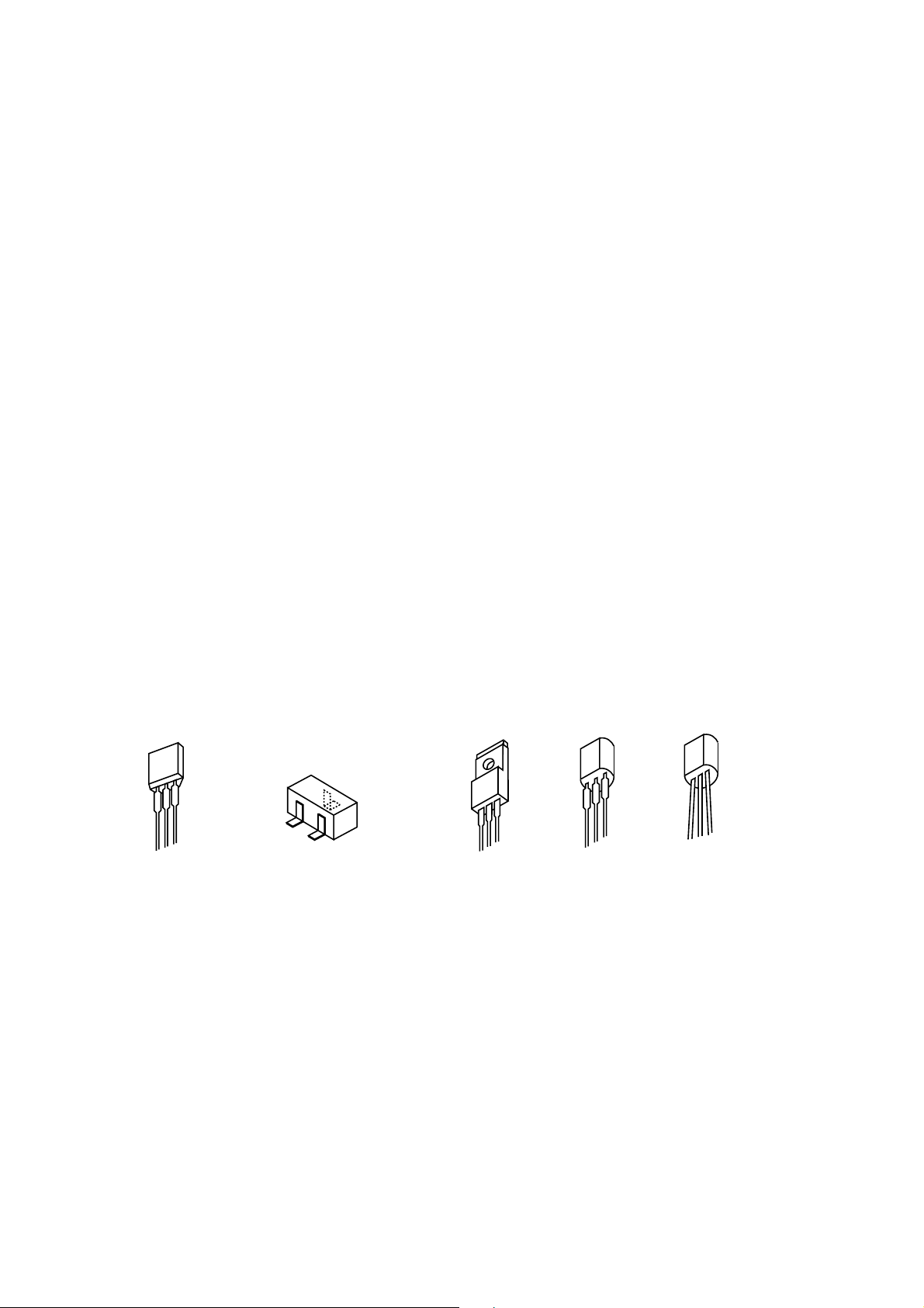
TRANSISTOR ILLUSTRATION
B
ECB
2SA933
CSC4115
2SA1162
2SC2712
2SC2714
DTA114YK
DTA123JK
DTA124XK
C
E
DTA144EK
DTC114EK
DTC114TK
DTC114YK
DTC124XK
RT1N144C
BC E
2SA1357
2SB1370
ECB
2SC1815
2SK2158
ECB
2SD65F
PE8550
8
Page 9
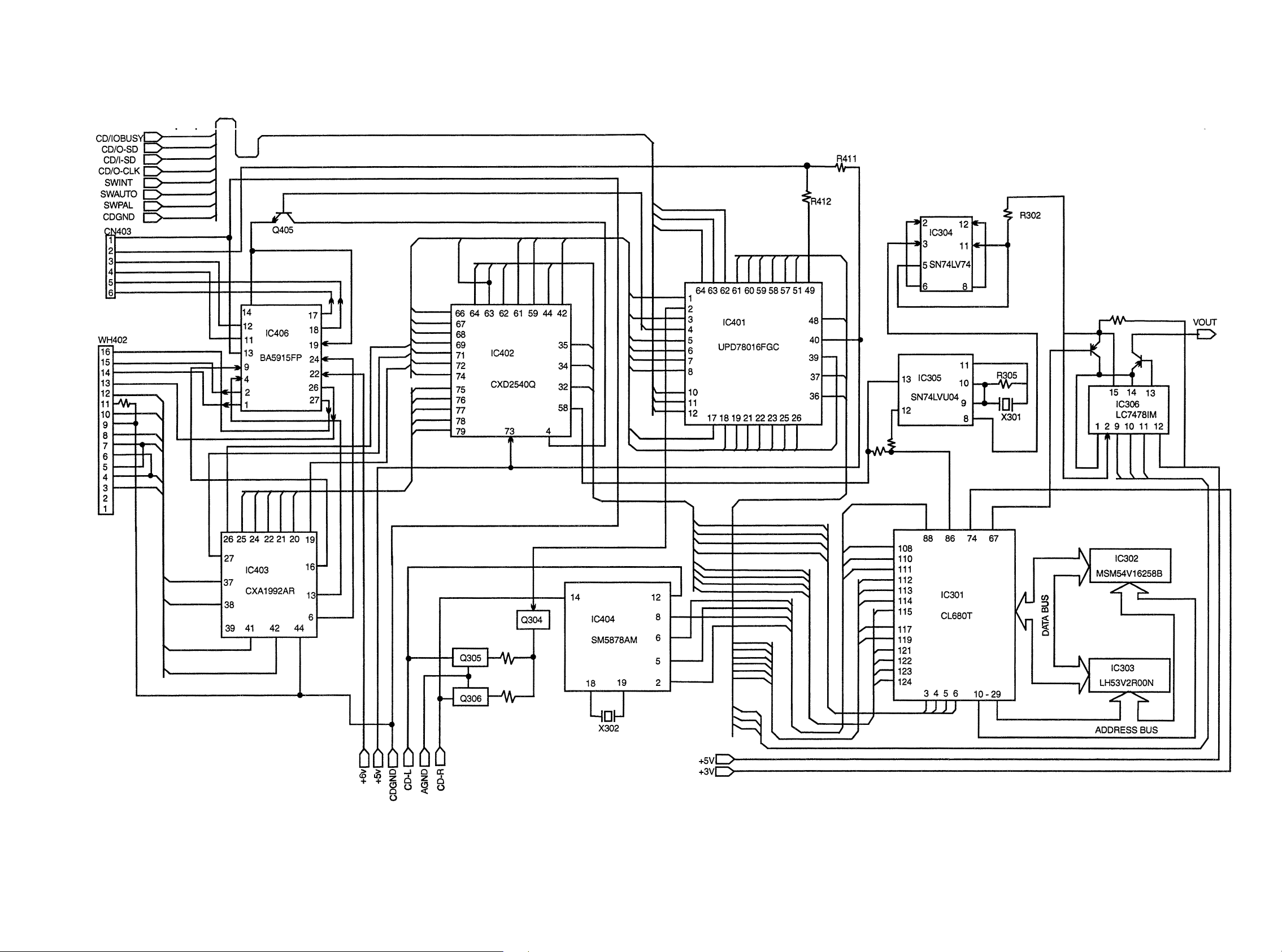
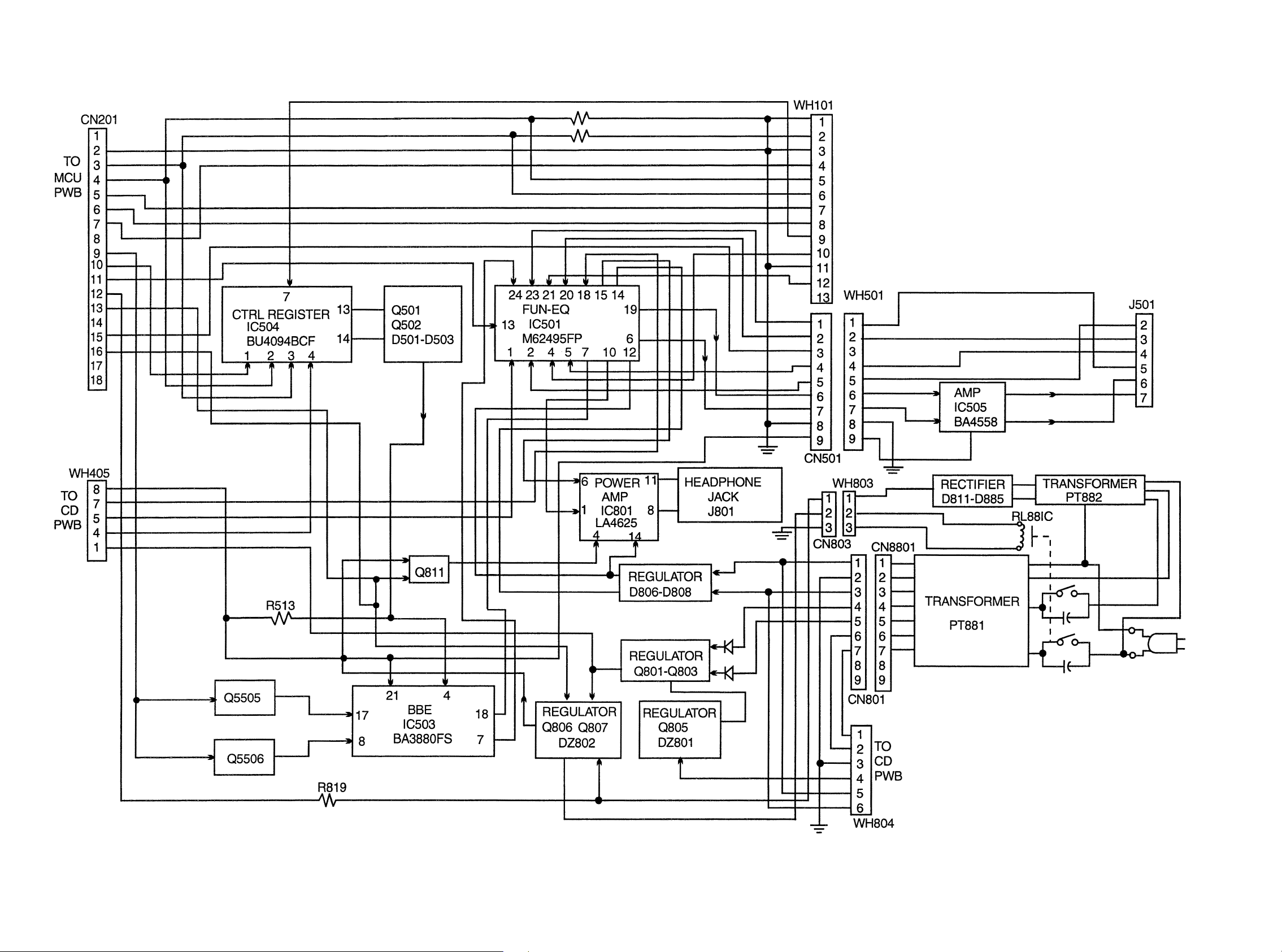
BLOCK DIAGRAM-1 (CD/CONTROL)
109
Page 10
BLOCK DIAGRAM-2 (POWER/AMP)
1211
Page 11
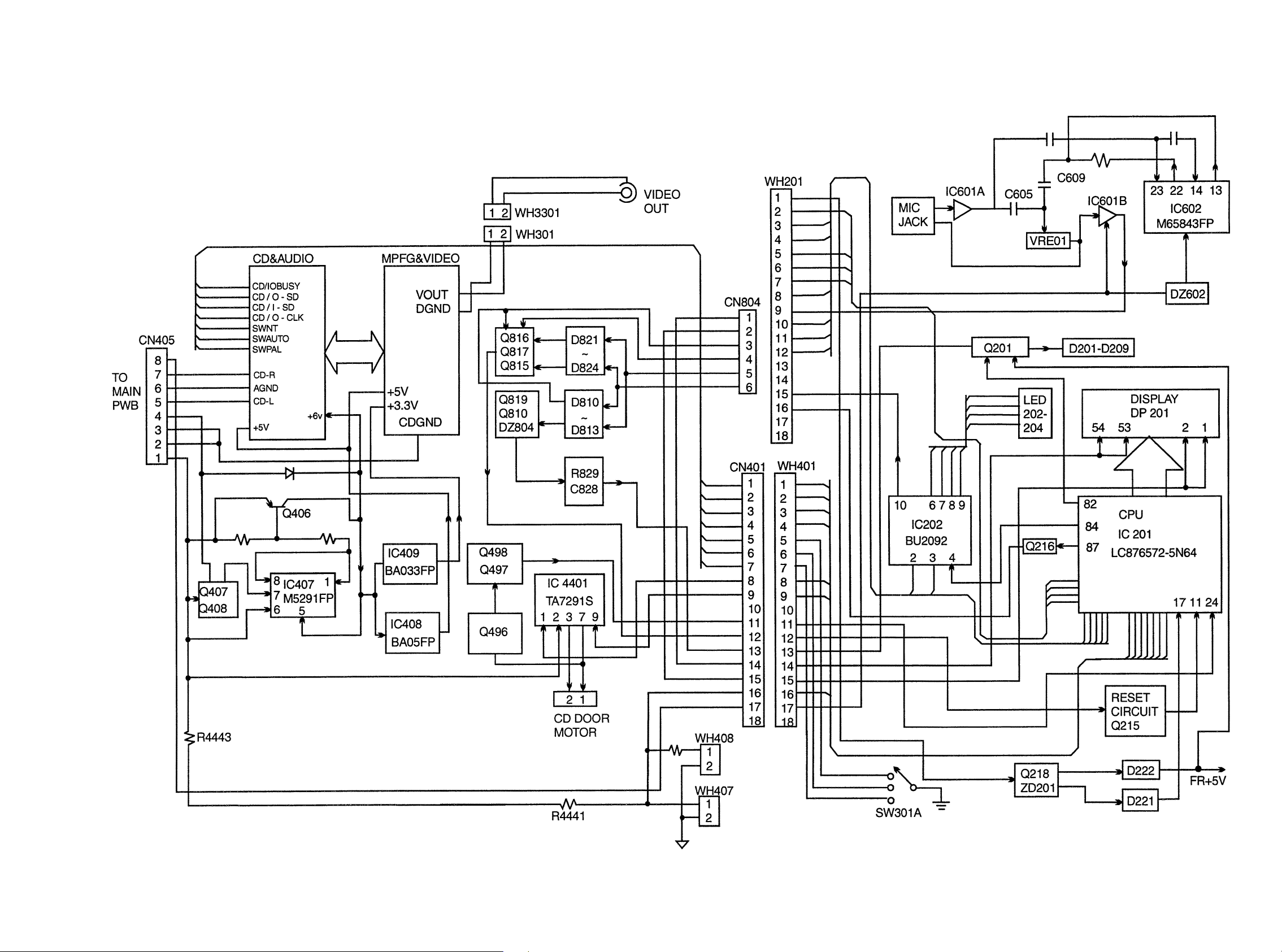
BLOCK DIAGRAM-3 (VIDEO/DISPLAY)
1413
Page 12
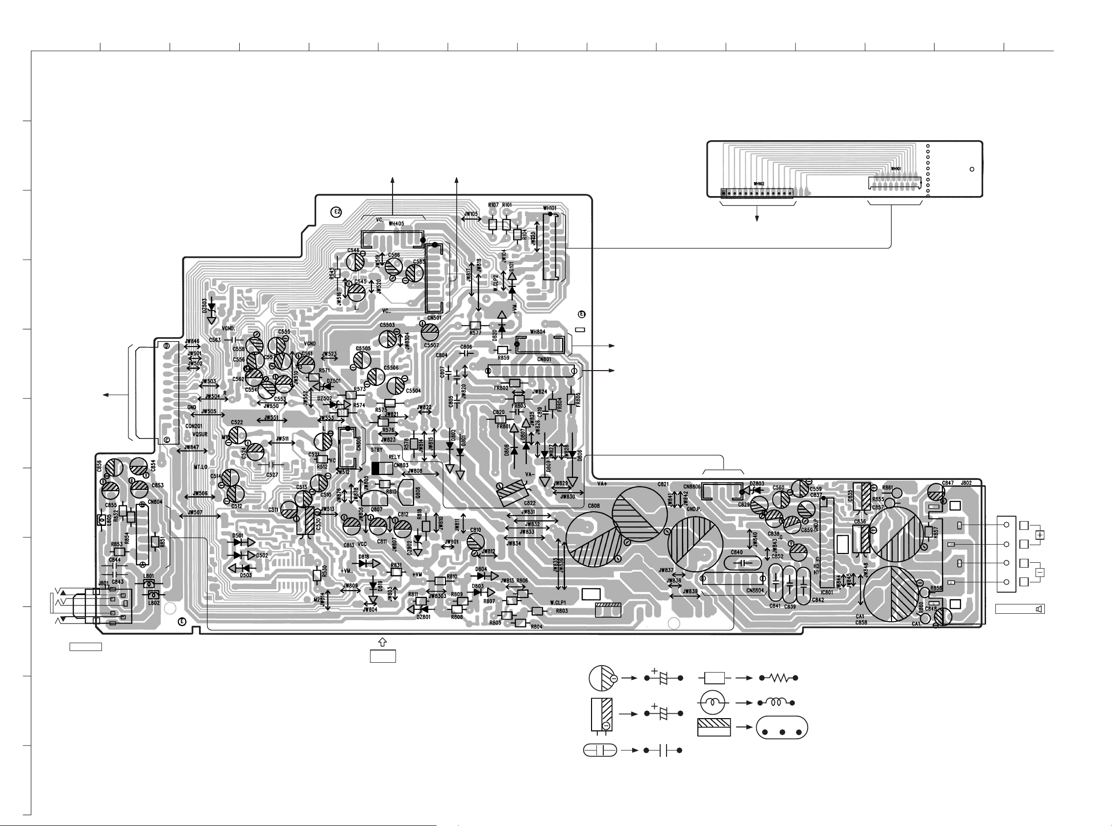
WIRING-1 (MAIN: COMPONENT SIDE)
1
A
234567
8
9
10
11 12 13
14
TUNER ADAPTOR C.B
(COMPONENT SIDE)
B
C
MAIN C.B
(COMPONENT SIDE)
TO VCD C.B
CN405
8
TO PT C.B
WH501
113
1
1
1
16
TO TUNER C.B
CN 701
116
D
9
1
E
WH201
TO DISPLAY C.B
F
1
9
18
1
6
1
TO VCD C.B CN804
TO PT C.B CN8801
5
1
3
B
G
1
6
ECB
C
E
H
BCE
Q801
I
J801
PHONES
CN803
13
TO PT C.B WH803
NOTE
5
1
16
1
L
R
L
14
R
SPEAKERS
J
ECB
ECB
K
1615
Page 13
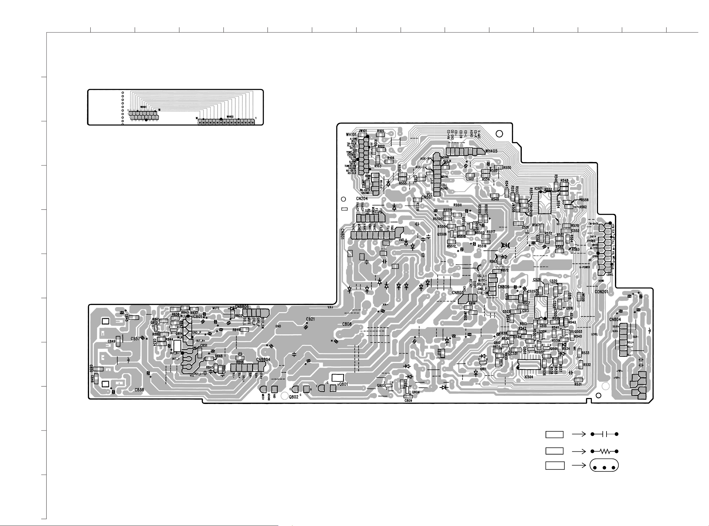
WIRING-2 (MAIN: CONDUCTOR SIDE)
1
A
234567
TUNER ADAPTOR C.B
(CONDUCTOR SIDE)
8
9
10
11 12 13
14
B
MAIN C.B
(CONDUCTOR SIDE)
C
D
24
1
13
12
E
F
1213
1
24
G
H
I
916
1
8
NOTE
CXXX
RXXX
J
C
E
B
E
C
B
K
1817
Page 14
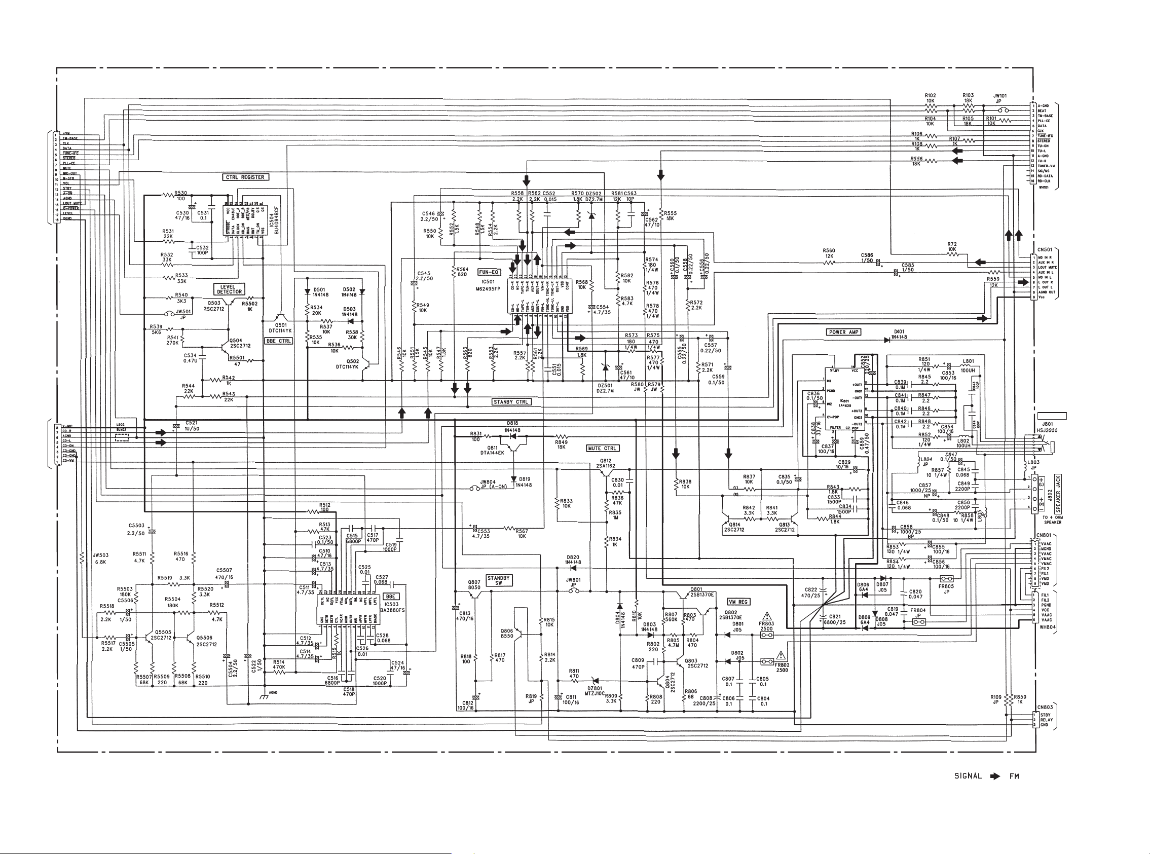
SCHEMATIC DIAGRAM-1 (MAIN)
MAIN C.B
CN201
TO DISPLAY C.B
TO VCD C.B (1/3)
WH201
CN405
WH405
TO TUNER ADAPTORTO PT C.B
WH501
PHONES
Q5505, 5506
MIC AMP
RELAY
DRIVER
MUTE MUTE
Q801-804
CN8801
TO PT C.B
CN804
TO VCD C.B
WH803
TO PT C.B
:
2019
Page 15
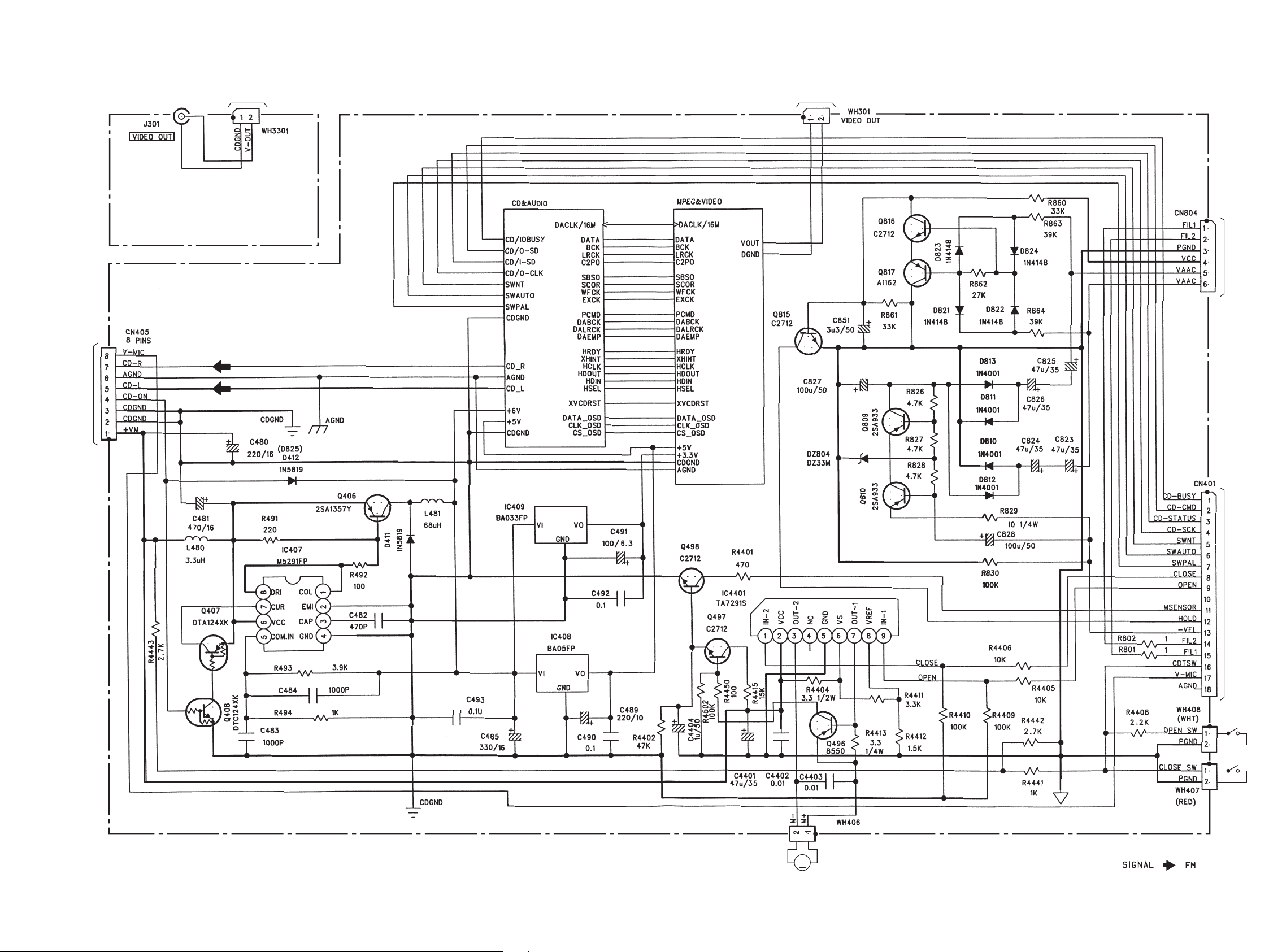
SCHEMATIC DIAGRAM-2 (VCD 1/3)
TO MAIN C.B
VIDEO OUT C.B
WH405
TO VCD C.B (1/3)
WH301
VCD C.B (1/3)
TO VIDEO OUT C.B
WH3301
SWITCH
Q816, 817
AC DETECT
WH804
TO MAIN C.B
Q407, 408
SWITCH
SWITCHING
SWITCHING
REGULATOR
+33V REG.
+5V REG.
Q497, 498
MSENSOR
SWITCH
MOTOR
DRIVER
Q809, 810
-VFL REG.
CURRENT
DETECT
TO DISPLAY C.B
S1
(OPEN)
S2
(CLOSE)
WH401
M
M1
(LOADING)
:
2221
Page 16
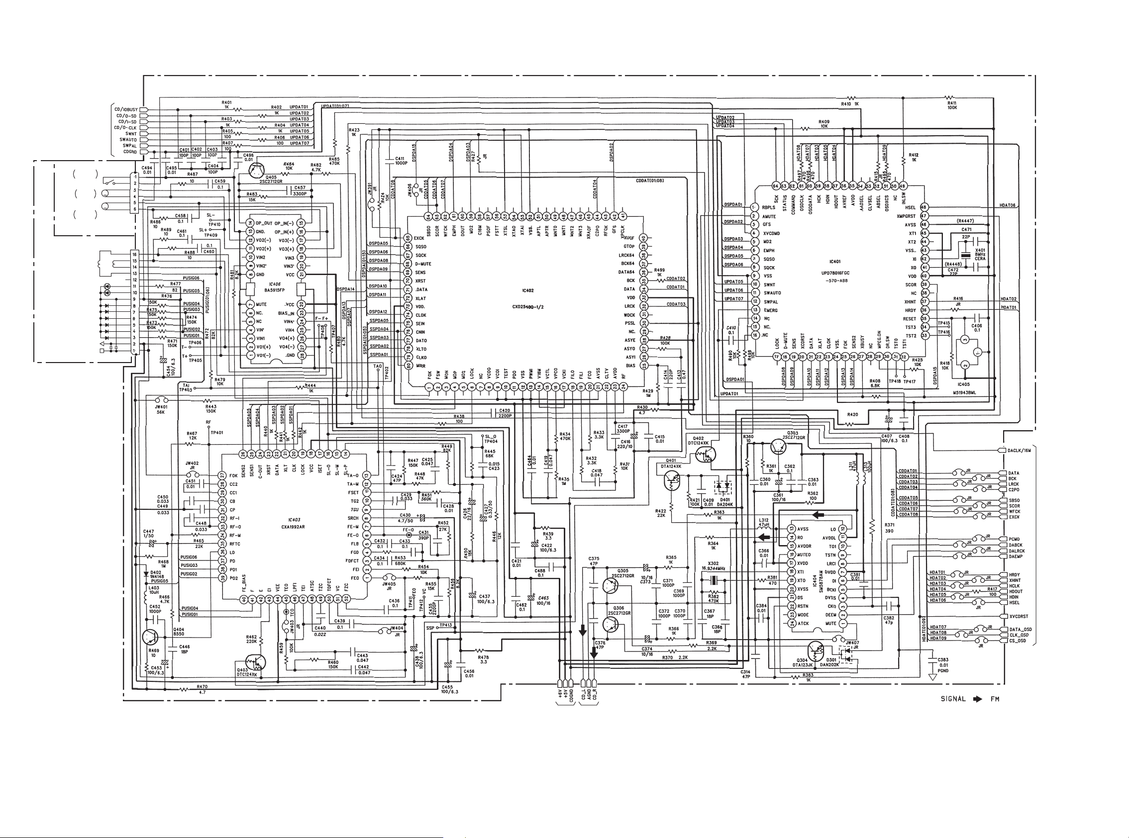
SCHEMATIC DIAGRAM-3 (VCD 2/3)
VCD C.B (2/3)
TO VCD C.B (1/3)
SW1
INSIDE
LIMIT SW
M2
SLED
MOTOR
M1
SPINDLE
MOTOR
MOTOR C.B
CD MECHANISM
DA-11T3C
OPTICAL PICK UP
BLOCK SF-P101 NR
M
M
COIL
TRACKING
FOCUS COIL
GND
SWIL
SL–
SL+
SP–
SP+
GND
VCC
PIN3
CN1
F–
T–
T+
F+
PD
VR
LD
F
C
B
A
D
E
VC
MOTOR DRIVER
SWITCH
CD DIGITAL SIGNAL PROCESSOR
CD SYSTEM
CONTROL
LD
DRIVER
SWITCH
CD RF SIGNAL PROCESSOR
SERVO AMP
MUTE
MUTE
SWITCH
SWITCH
RIPPLE
FILTER
OR GATE
D/A CONVETOR
RESET
TO VCD C.B (3/3)
TO
VCD C.B
(3/3)
TO
MAIN C.B
WH405
:
2423
Page 17
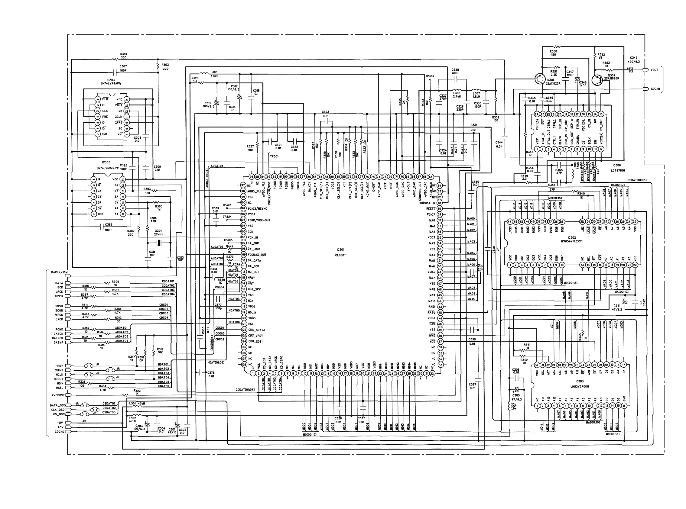
SCHEMATIC DIAGRAM-4 (VCD 3/3)
VCD C.B (3/3)
DIVIDER
INV. BUFFER
BUFFER
BUFFER
TO VCD C.B (1/3)
CHARACTOR DISPLAY CONTROL
DRAM
TO VCD C.B (2/3)
DSP
EEPROM
2625
Page 18
WIRING-3 (VCD: COMPONENT SIDE)
14
PICK UP ASSY
SF-P101NR
13 12 11 10 9 8
7
6
5
432
1
A
V-OUT C.B
VIDEO OUT
B
VCD C.B
(COMPONENT SIDE)
BCE
BCE
1
16
1
BCE
TO MAIN C.B
1
WH405
8
14
1
7
C
8
1
2
D
7
1
14
8
1
45
E
8
C
B
33
11
2
1
2
1
6
1
2
1
S1
(OPEN)
S2
(CLOSE)
TO MAIN C.B
WH804
E
1
WH401
TO DISPLAY C.B
F
24
16
16
1
3
2
18
NOTE
C
B
EEC
B
1
12 13
E
C
9
B
1
M1
(LOADING)
M
G
MOTOR C.B
M2
+
_
PIN3
M2
(SLED MOTOR)
SW1
(INSIDE LIMIT SW)
(SPINDLE MOTOR)
SW1
_
M1
M1
H
+
I
J
2827
Page 19

WIRING-4 (VCD: CONDUCTOR SIDE)
1
234567
8
9
10
11 12 13
14
A
B
VCD C.B
C
D
(CONDUCTOR SIDE)
E
F
1
32
28
G
16
17
1415
1617
1
32
33
48
1
64
49
H
NOTE
I
CXXX
RXXX
C
J
B
EEC
B
3029
Page 20

WIRING-5 (TUENR)
1
A
B
C
D
234567
8
9
10
11 12 13
14
TO TUNER ADAPTOR C.B
WH102
E
F
G
H
I
J
K
3231
Page 21

SCHEMATIC DIAGRAM-5 (TUNER)
IF AMP
BAND
SW
TO TUNER ADAPTOR C.B
WH102
TUNER C.B
TU+B
SW
FM/AM IF/STEREO
TUNER SYSTEM
L771
DC Balance/Mono Distortion ADJ
L772
AM IF ADJ
L981
AM T racking ADJ
:
:
3433
Page 22

WIRING-6 (DISPLAY: COMPONENT SIDE)
14
13 12 11 10 9 8
DISPLAY C.B
(COMPONENT PART)
7
MD
6
5
432
1
A
B
C
D
CONTROL C.B
(COMPONENT SIDE)
E
MIC JACK C.B
(COMPONENT SIDE)
NOTE
ECB
ECB
F
G
H
I
J
3635
Page 23

WIRING-7 (DISPLAY: CONDUCTOR SIDE)
1
A
B
234567
8
9
10
11 12 13
14
DISPLAY C.B
(CONDUCTOR PART)
C
D
CONTROL C.B
(CONDUCTOR SIDE)
E
F
TO VCD C.B
G
H
I
J
NOTE
CXXX
RXXX
B
C
EEC
B
CN401
TO MAIN C.B
CN201
3837
Page 24

SCHEMATIC DIAGRAM-6 (DISPLAY)
J601
MIC
TO MAIN C.B
CN201
DISPLAY C.B
IC601
MIC AMP/ECHO AMP
6.8K 6.8K
4.7U 4.7U
1.2K
1.2K
DIGITAL
ECHO
MTZJ6.8B
SPR-39MVWF
SPR-39MVWF
SPR-39MVWF
SPR-39MVWF
SPR-39MVWF
LED DRIVER
DECODER
R
2.2K
2.2K
R
R
DRIVER SW
2.2K
R
SW
SW
R
CN401
TO VCD C.B (1/3)
VOL/MULTI JOG
BUFFER
SYSTEM/
DISPLAY CONTROL
2.2/50
2.2K
1.2K 1.2K
1.5K
MD
CD AUX TUNER DISPLAY
(CD LED)
LED DRIVER
POWERDEMO
1N4148
REG.
RESET
2.2K
330/6.3
RECEIVER
6.8K 4.7K
3.3K
CD OPENREW FF
CONTROL C.B
2.2K 2.2K 1.5K 1.2K 1.2K
220/10
STOPPLAYPAUSEENTERJOG MODE
4039
Page 25

WIRING-8 (PT)
MD IN
AUX IN
LINE OUT
J501
L R
7
654321
PT C.B
(COMPONENT SIDE)
PT882
1
9
TO MAIN C.B
CN501
5
4
1
8
1
A
A
2
3
456
7
PT C.B
(CONDUCTOR SIDE)
B
B
C
C
TO MAIN C.B
CN803
3
1
D
D
WH803
120V
220V
240V
PT881
E
E
9
F
F
CN801
TO MAIN C.B
1
G
G
H
H
I
CN8801
120V/220-240V
50/60Hz
I
J
J
4241
Page 26

SCHEMATIC DIAGRAM-7 (PT)
PT C.B
LINE
AMP
MUTE
DRIVE
TO MAIN C.B
CN501
MUTE
DRIVE
2S
MUTE
MUTE
Q881, Q882
POWER OFF
DISCHARGE
MUTE
MUTE
BABY PT
!
!
MAIN PT
TO MAIN C.B
TO MAIN C.B
CN803
!
CN801
4443
Page 27

VOLTAGE CHART
45
Page 28

4647484950
Page 29

Page 30

Page 31

Page 32

Page 33

FL (13-ST-36GNAK) GRID ASSIGNMENT/ANODE CONNECTION
5251
Page 34

ELECTRICAL ADJUSTMENT
< TUNER SECTION >
1
L771
IC771
TP4
R785
TP3
PRACTICAL SERVICE FIGURE
1. DC Balance/Mono Distortion Adjustment
Settings: • Test point: TP3, TP4
• Adjustment location: L771
• Input level: 54dB
2
L772
TP1
5
FFE801
TUNER C.B
3
30
TP2
L981
Method: Set to FM 98.0MHz and adjust L771 so that
the voltage between TP3 and TP4 becomes
0V±0.04V.
Next, check that the distortion is less than
1.3%.
2. AM IF Adjustment
Settings: • Test point: TP5, TP6
L772 ..............................................450kHz
3. AM Tracking Adjustment
Settings: • Test point: TP5, TP6
• Adjustment location: L981
Method: Set to AM 999kHz and adjust L981 so that the
test point becomes maximum.
4. AM VT Check
Settings: • Test point: TP1 (VT)
Method: Set to AM 1710kHz and check that the test
point is less than 7.0V.
Then set to AM 530kHz and check that the test
point is more than 0.5V.
< TUNER SECTION >
<FM SECTION>
IHF Sensitiviy: 4dB±6dB
(THD 3%) (at 88.0/98.0MHz)
5dB±6dB (at 108MHz)
Signal to noise ratio: More than 65dB
(at 98.0MHz)
Distortion: Less than 1.5%
(Input: 66dB) (at 98.0MHz)
Stereo separation: More than 25dB
(at 98.0MHz)
Intermediate frequency: 10.7MHz
<AM SECTION>
Sensitivity: Less than 60dB (at 603kHz)
(S/N 20dB) Less than 58dB
(at 999/1404kHz)
Signal to noise ratio: More than 36dB
(Input: 74dB) (at 999kHz)
Distortion: Less than 2.0%
(at 999kHz)
Intermediate frequency: 450±5kHz
TP6
GND
12 11 10
TP5
CN701
5. Clock Frequency Check
Settings: • Test point: TP2 (CLK IC771 pin30)
Method: Set to AM 1710kHz and check that the test
point becomes 2160kHz±45Hz.
6. FM VT Check
Settings: • Test point: TP1 (VT)
Method: Set to FM 88MHz, 108.0MHz and check that
the test point is more than 0.5V (88MHz) and
less than 8.0V (108.0MHz).
5453
Page 35

IC DESCRIPTION
IC, LC876572V-5N64
Pin No. Pin Name I/O Description
1
2
3
4
5
6
_______________
I-STEREO
I-TUDO/
I-STATUS
I/O-BUSY
___________
O-F.LED
O-M.STB
O-CLK
I/O
O
O
O
I
Connected to stereo detection and tuner.
Connected to tuner PLL IC LC72131 pin-6 DO and connected to VCD µPD78016
I
pin- .
63
Connected to VCD microprocessor µPD78016 pin-≥.
Function LED control output.
Connected to main shift resistor 4094 pin-1 STB.
Connected to front shift resistor BU2092 pin-3 CLK, main shift resistor 4094 pin-3
CLK, and tuner PLL IC LC72131 pin-5 CL.
7
O-DATA
Connected to front shift resistor BU2092 pin-2 DATA, main shift resistor 4094 pin-
O
2 DATA, and tuner PLL IC LC72131 pin-4 DI.
8
9
10
11
12
13
14
15
16
17
O-VOLCTL
I-TMBASE
_____________
O-CKSFT
RESET
I-ACOFF
N.C
VSS
CF1
CF2
VDD1
O
O
I/O
—
—
—
—
—
Connected to VOL/P.EQ IC M62439SP pin-! CONT.
I
Reference clock input for clock PLL IC LC72131 pin-7.
Clock shift output is shifted: “L”
Microprocessor reset.
I
Hold status detection.
Not connected.
GND.
Connected to 5.76 MHz oscillator
Connected to 5.76 MHz oscillator.
Microprocessor power supply. (µ-com 5 V)
18
19
20
21
22
23
24
25
26
27
28
29
30-42
43-45
46
47-50
51
52-63
64
65
N.C
I-KEY1
I-KEY0
I-DSW
I-CDTSW
I-ENC1
M SENSOR
O-CE
N.C
I-LEVEL
O-CLK
I-RMT
G1-G13
P33-P35
VDD3
P29-P32
VP
P17-P28
________
P16/BBE
______________
P15/DOLBY
—
Not connected.
I
Key AD value input.
I
Key AD value input.
I
Deck MECA status detection input. (AD)
I
CD tray OPEN/CLOSE status detection input. (AD)
I
AD value input from multiple jog rotary encoder outputs A and B.
I
Electronic VOL’s AD value input from rotary encoder outputs A and B.
O
Connected to tuner PLL IC LC72131 pin-3 CE.
—
Not connected.
I
Level meter input.
O
Connected to VCD microprocessor µPD78016 pin- .
I
Remote control input.
O
FL tube grid output.
O
FL tube anode output.
—
Microprocessor power supply. (µ-com 5 V)
O
FL tube anode output.
—
Connected to minus power supply for FL, -VFL.
O
FL tube anode output.
O
FL tube anode output, and INT.DIODE MATRIX input.
O
FL tube anode output, and INT.DIODE MATRIX input.
64
66
P14/AM10k
O
FL tube anode output, and INT.DIODE MATRIX input.
55
Page 36

Pin No. Pin Name I/O Description
67
68
69
P13/FMWIDE&AMST
P12/LW
P11/SW
FL tube anode output, and INT.DIODE MATRIX input.
O
FL tube anode output, and INT.DIODE MATRIX input.
O
FL tube anode output, and INT.DIODE MATRIX input.
O
70
71
72
73-78
79
80
81
82
83
84
85
86
87
88
89
90
91
92
93
94
P10/OIRT
P9/RDS
VDD4
P3-P8
P2/CAM
P1/AUTO
O-QSURR
O-SWSCAN
O-MOTOR
O-FSTB
O-CDOPEN
O-CDCLOSE
O-POWER
______________
O-MDRST
VSS2
VDD2
O-SD
O-CLK
O-MUTE
_____
O-PL
—
—
—
FL tube anode output, and INT.DIODE MATRIX input.
O
FL tube anode output, and INT.DIODE MATRIX input.
O
Microprocessor power supply. (µ-com 5 V)
FL tube anode output. (SHOP)
O
Deck mechanism status detection input. (CAM)
O
Deck mechanism status detection input. (AUTO)
O
Q-Surround IC control output.
O
Key scan detection timing switch.
O
Deck mechanism motor control output.
O
Connected to front shift resistor IC BU2092 pin-5.
O
CD tray open control output.
O
CD tray close control output.
O
Power supply ON/OFF control.
O
MD unit 7ZG-9A reset signal output.
O
GND.
Microprocessor power supply. (µ-com 5 V)
Connected to VCD microprocessor µPD78016 pin- .
O
Connected to VCD microprocessor µPD78016 pin- .
O
Main mute output.
O
Deck mechanism plunger solenoid control output.
O
62
64
95-100
N.C
—
Not connected.
56
Page 37

IC, CL680
Pin No. Pin Name I/O Description
1
2
3
NC
VSS
CD BCK
—
No connection.
—
GND.
I
Bit clock input from CD DSP.
4
5
6
7-9
10-15
16
17
18
19
20
21
22
23-29
30-36
37
38
39
40
41
42
43
44-46
47
48
CD DATA
CD LRCK
CD C2PO
NC
MD0-MD5
VSS
MD6
VDD3
MD7
VSS
MD8
VDD3
MD9-MD15
NC
________
MCE
__________
MWE
VSS
________
CAS
VDD3
___________
RASO
___________
RASI
MA10-MA8
VSS
MA7
—
I/O
—
I/O
—
I/O
—
I/O
—
I/O
—
—
O
—
O
—
O
O
O
—
O
I
Data input from CD DSP.
I
LRCK input from CD DSP.
I
C2 pointer input from CD DSP.
No connection.
DRAM/ROM interface. (DATA)
Ground.
DRAM/ROM interface. (DATA)
Power supply 3.3V.
DRAM/ROM interface. (DATA)
Ground.
DRAM/ROM interface. (DATA)
Power supply 3.3V.
DRAM/ROM interface. (DATA)
No connection.
ROM chip enable.
DRAM write enable.
Ground.
DRAM/ROM interface.
Power supply 3.3V.
DRAM/ROM interface.
DRAM/ROM interface. (Address)
Ground.
DRAM/ROM interface. (Address)
49
50-52
53
54
55
56-58
59
60
61
62-64
65
66
67
68
VDD3
MA6-MA4
VSS
MA3
VDD3
MA2-MA0
PGIO7
______________
RESET
VDD MAX IN
NC
AGND DAC
A DAC
COMP OUT
AGND DAC
—
O
—
O
—
O
I/O
—
—
—
—
O
—
Power supply 3.3V.
DRAM/ROM interface. (Address)
Ground.
DRAM/ROM interface. (Address)
Power supply 3.3V.
DRAM/ROM interface. (Address)
Programmable I/O.
I
Reset input.
Power supply - VDDMAX. (5.0V)
No connection.
Analog ground.
Analog power supply (DAC) : 3.3V.
Composite out.
Analog ground.
57
Page 38

Pin No. Pin Name I/O Description
Video signal “Y” OUT.
—
—
—
—
—
—
O
Analog power supply (DAC) 3.3V.
Analog ground.
Reference resistor input.
I
Voltage reference input.
I
Analog power supply (DAC) : 3.3V.
Video signal “C” out.
O
Analog ground.
Clock selection input.
I
Ground.
Clock selection input.
I
Power supply 3.3V.
Clock selection input.
I
69
70
71
72
73
74
75
76
77-79
80
81
82
83, 84
Y OUT
AVDD DAC
AGND DAC
R REF
V REF
AVDD DAC
C OUT
AGND DAC
CLK SEL0-2
VSS
CLK SEL3
VDD3
CLK SEL4, 5
85
86
87
88
89, 90
91
92
93
94
95
96
97
98
99
100
101
102
103
104
AGND PLL
DA XCK
AVDD PLL
DA EMP
PGIO5, O6
PGIO0
PGIO8
______________ ______________
VSYNC/CSYNC
AVDD PLL
VID_DAC_CK
PROC_CK
AUD_XCK
AGND PLL
VSS
NC
______________
HSYNC
VDD3
VCK OUT
VSS
—
—
O
I/O
I/O
I/O
O
—
O
O
O
—
—
—
O
—
O
—
Analog ground.
DA XCK (16.933MHz) input.
I
Analog power supply 3.3V.
DAC-emphasis output.
Programmable I/O.
______________ ______________
VSYNC/CSYNC output.
Analog power supply (PLL) 3.3V.
Video DAC clock.
Processor clock.
Audio XCK.
Analog ground.
Ground.
No connection.
______________
HSYNC output.
Power supply 3.3V.
VCK out.
Ground.
105
106
107
108
109
110
111
112
113
GCK
VCK
GCK OUT
DA LRCK
VDD MAX OUT
DA DATA
DA BCK
HD OUT
HRDY
—
Global clock signal input. (42.3MHz)
I
Video clock signal input. (27.0MHz)
I
Global clock signal output. (27.0MHz)
O
DAC-LRCK output.
O
Power supply (VDD MAX) : 5.0V.
DAC-PCM data output.
O
DAC-BIT clock output.
O
Micon interface. (Data out)
O
Micon interface. (Host ready)
O
58
Page 39

Pin No. Pin Name I/O Description
__________
114
115
HINT
CDG SCK
Micon interface. (Host interrupt)
O
CD-G serial clock input.
I
116
117
118
119
120
121
122
123
124
125
126-128
VSS
HCK
VDD3
HD IN
VDD3
HSEL
CDG DATA
CDG VFSY
CDG SOSI
DSP-XCK
NC
Ground.
—
Micon interface. (Host clock)
I
Power supply 3.3V.
—
Micon interface. (Host data in)
I
Power supply 3.3V.
—
Micon interface. (Host select in)
I
CD-G data input.
I
CD-G VFSY input.
I
CD-G SOSI input.
I
DSP-XCK output.
O
No connection.
—
59
Page 40

IC, µPD78016FGC-570-AB8
Pin No. Pin Name I/O Description
1
2
3
RBPLS
AMUTE
GFS
RADIAL BALANCE PLUS.
O
AUDIO ANALOG MUTE (H=MUTE ON).
O
GFS.
I
10
11
12
13
14
15
16
17
18
19
20
21
22
4
5
6
7
8
9
XVCDMD
MD2
EMPH
SQSO
SQCK
VSS
SWNT
SWAUTO
SWPAL
EMERG
NC
LPCSEL
NC
LOCK
DMUTE
SENS
XCDRST
DATA
XLAT
—
—
—
AUDIO/VIDEO CD MODE (L=VCD=SPINDLE GAIN UP).
I
DOUT MUTE CONT.
O
EMPHASIS.
I
SQDATA FROM CD.
I
SQCLK TO CD.
O
GND.
SW TV OUT MODE (L=NTSC).
I
SW TV OUT MODE (L=NTSC/PAL AUTO).
I
SW TV OUT MODE (L=PAL).
I
POWER EMERGENCY STOP (L*3sec=STOP).
I
Not used.
“LPC ON/OFF (H=ON, NORMAL)”.
I
Not used.
GFS (FRAME SYNC) LOCK (NO USE=H).
O
DIGITAL DATA OUT MUTE.
O
DSP SENS1 FROM CD.
I
CD RESET.
O
DATA TO CD.
O
XLT TO CD.
O
23
24
25
26
27
28
29
30
31
32
33
34
35
36
37
38
39
40
CLOK
VSS
FOK
SENS2
XBUSY
NC
NC
NC
TST0
TST1
TST2
TST3
RESET
HRDY
XHINT
NC
SCOR
VDD
O
—
I/O
—
—
—
I/O
I/O
I/O
I/O
—
—
CLK TO CD.
GND.
FOCUS OK.
I
SSP SENS2 FROM CD.
I
READY/BUSY I/O TO HOST OD.
Not used.
CHECK LAND.
RESET.
I
HRDY FROM CL680.
I
HINT FROM CL680.
I
Not used.
SCOR FROM CD.
I
5.0VDD.
41
XO
8.0MHz CERALOCK.
O
60
Page 41

Pin No. Pin Name I/O Description
42
43
44
XI
VSS
XT2
8.0MHz CERALOCK.
I
GND.
—
Not used.
—
45
46
47
48
49
50
51
52
53
54
55
56
57
58
59
60
61
62
63
XT1
AVSS
XMPGRST
HSEL
INLSW
NC
OSDXCS
ABSEL
CLVSEL
AADSEL
AVDD
AVREF
HDOUT
HDIN
HCK
OSDDATA
OSDCLK
COMMAND
STATUS
5.0VDD.
I
GND.
—
MPEG BLOCK IC RESET.
O
ADDRESS/DATA SEL TO CL680.
O
INSIDE LIMIT SW.
I
Not used.
—
OSD CHIP SELECT.
O
CXA1992A/B SELECT (L=CXA1992A).
I
CLV MODE SELECT (H=CLV-N).
I
AUTO ADJUST SELECT (H=AUTO ON).
I
—
5.0VDD.
—
HD-OUT FROM CL680.
I
HD-IN TO CL680.
O
HCK TO CL680.
O
OSD DATA.
O
OSD CLOCK.
O
COMMAND FROM HOST.
I
STATUS TO HOST.
O
64
SCK
SCK FROM HOST.
I
61
Page 42

IC, CXD2540Q
Pin No. Pin Name I/O Description
1
2
3
FOK
FSW
MON
I
Focus OK input. Used for SENS output and the servo auto sequencer.
O
Spindle motor output filter switching output.
O
Spindle motor on/off control output.
10
11
12
13
14
15
16
17
18
19
20
21
22
4
5
6
7
8
9
MDP
MDS
LOCK
NC
VCOO
VCOI
TEST
PDO
VSS
PWMI
V16M
VCTL
VPCO
VCKI
FILO
FILI
PCO
AVSS
CLTV
—
—
—
O
Spindle motor servo control.
O
High, when sampled value of GFS at 460Hz is high.
O
Low, when sampled value of GFS at 460Hz is low by 8 times successively.
O
Analog EFM PLL oscillation circuit output.
I
Analog EFM PLL oscillation circuit input. fLOCK=8.6436MHz.
I
TEST pin.
O
Analog EFM PLL charge pump output.
GND.
I
Spindle motor external control input.
O
VCO2 oscillation output for the wide-band EFM PLL.
I
VCO2 control voltage input for the wide-band EFM PLL.
O
Wide-band EFM PLL charge pump output.
I
VCO2 oscillation input for the wide-band EFM PLL.
O
Multiplier PLL (slave=digital PLL) filter output.
I
Multiplier PLL filter input.
O
Multiplier PLL charge pump output.
Analog GND.
I
Multiplier VCO1 control voltage input.
23
24
25
26
27
28
29
30
31
32
33
34
35
36
37
38
AVDD
RF
BIAS
ASYI
ASYO
ASYE
NC
PSSL
WDCK
LRCK
VDD
DA16
DA15
DA14
DA13
DA12
—
—
—
Analog power supply (5V).
I
EFM signal input.
I
Constant current input of the asymmetry circuit.
I
Asymmetry comparator voltage input.
O
EFM full-swing output.
I
Low: asymmetry circuit off; high: asymmetry circuit on.
I
Audio data output mode switching input. Low: serial output; high: parallel output.
O
D/A interface for 48-bit slot. Word clock f=2Fs.
O
D/A interface for 48-bit slot. LR clock f=Fs.
Power supply (5V).
DA16 (MSB) output when PSSL=1.
O
48-bit slot serial data (two’s complement, MSB first) when PSSL=0.
O
DA15 output when PSSL=1. 48-bit slot bit clock when PSSL=0.
DA14 output when PSSL=1.
O
64-bit slot serial data (two’s complement, LSB first) when PSSL=0.
O
DA13 output when PSSL=1. 64-bit slot bit clock when PSSL=0.
O
DA12 output when PSSL=1. 64-bit slot LR clock when PSSL=0.
62
Page 43

Pin No. Pin Name I/O Description
39
40
41
DA11
DA10
DA09
O
DA11 output when PSSL=1. GTOP output when PSSL=0.
O
DA10 output when PSSL=1. XUGF output when PSSL=0.
O
DA09 output when PSSL=1. XPLCK output when PSSL=0.
42
43
44
45
46
47
48
49
50
51
52
53
54
55
56
57
58
59
60
DA08
DA07
DA06
DA05
DA04
DA03
DA02
DA01
APTR
APTL
VSS
XTAI
XTAO
XTSL
FSTT
FSOF
C16M
MD2
DOUT
O
DA08 output when PSSL=1. GFS output when PSSL=0.
O
DA07 output when PSSL=1. RFCK output when PSSL=0.
O
DA06 output when PSSL=1. C2PO output when PSSL=0.
O
DA05 output when PSSL=1. XRAOF output when PSSL=0.
O
DA04 output when PSSL=1. MNT3 output when PSSL=0.
O
DA03 output when PSSL=1. MNT2 output when PSSL=0.
O
DA02 output when PSSL=1. MNT1 output when PSSL=0.
O
DA01 output when PSSL=1. MNT0 output when PSSL=0.
Aperture compensation control output.
O
This pin outputs a high signal when the right channel is used.
Aperture compensation control output.
O
This pin outputs a high signal when the left channel is used.
—
GND.
I
Crystal oscillation circuit input.
O
Crystal oscillation circuit output.
I
Crystal selector input.
O
2/3 frequency divider output for Pins 53 and 54.
O
1/4 frequency divider output for Pins 53 and 54.
O
16.9344MHz output. (V16M output in CLV-W and CAV-W modes)
I
Digital-out on/off control. High: on; low: off
O
Digital-out output.
61
62
63
64
65
66
67
68
69
70
71
72
73
74
75
76
EMPH
WFCK
SCOR
SBSO
EXCK
SQSO
SQCK
MUTE
SENS
XRST
DATA
XLAT
VDD
CLOK
SEIN
CNIN
Outputs a high signal when the playback disc has emphasis, and a low signal when
O
there is no emphasis.
I
WFCK (write frame clock) output.
O
Outputs a high signal when either subcode sync S0 or S1 is detected.
O
Sub P to W serial output.
I
SBSO readout clock input.
O
Sub Q 80-bit and PCM peak, level metter and internal status outputs.
I
SQSO readout clock input.
I
High: mute; low: release
—
SENS output to CPU.
I
System reset. Reset when low.
O
Serial data input from CPU.
O
Latch input from CPU. Serial data is latched at the falling edge.
—
Power supply (5V).
O
Serial data transfer clock input from CPU.
I
SENS input from SSP.
I
Track jump count signal input.
63
Page 44

Pin No. Pin Name I/O Description
77
78
79
DATO
XLTO
CLKO
Serial data output to SSP.
O
Serial data latch output to SSP. Latched at the falling edge.
O
Serial data transfer clock output to SSP.
O
80
Notes)
• The 64-bit slot is an LSB first, two’s complement output, and the 48-bit slot is an MSB first, two’s complement output.
• GTOP is used to monitor the frame sync protection status. (High: sync protection window open.)
• XUGF is the negative pulse for the frame sync obtained from the EFM signal. It is the signal before sync protection.
• XPLCK is the inverse of the EFM PLL clock. The PLL is designed so that the falling edge and the EFM signal transition point
coincide.
• GFS goes high when the frame sync and the insertion protection timing match.
• RFCK is derived from the crystal accuracy, and has a cycle of 136µ.
• C2PO represents the data error status.
• XRAOF is generated when the 32K RAM exceeds the ±28F jitter margin.
MIRR
Mirror signal input. Used when the number of tracks is 128 or more for the 2N-track
I
jump and M track move of the auto sequencer.
64
Page 45

IC, CXA1992AR
Pin No. Pin Name I/O Description
1
2
3
FEO
FEI
FDFCT
Output terminal for focus error amplifier. Internally connected to window comparator
O
input for bias condition.
Input terminal for focus error.
I
Capacitor connection terminal for time constant used when there is defect.
I
10
11
12
13
14
15
16
4
5
6
7
8
9
FGD
FLB
FE_O
FEM
SRCH
TGU
TG2
FSET
TA_M
TA_O
SL_P
SL_M
SL_O
This pin is connected to GND via capacitor when high frequency gain of the focus
I
servo is attenuated.
This is a pin where the time constant is externally connected to raise the low frequency
I
gain of the focus servo.
Focus drive output.
O
Focus amplifier inverted input pin.
I
This is a pin where the time constant is externally connected to generate the focus
I
search waveform.
This is a pin where the selection time constant is externally connected to set the
I
tracking servo the high frequency gain.
This is a pin where the selection time constant is externally connected to set the
I
tracking high frequency gain.
Pin for setting peak of the phase compensator of the focus tracking.
I
Tracking amplifier inverted input pin.
I
Tracking drive output.
O
Sled amplifier non-inverted input pin.
I
Sled amplifier inverted input pin.
I
Sled drive output.
O
17
18
19
20
21
22
23
24
25
26
27
28
29
30
31
ISET
Vcc
LOCK
CLK
XLT
DATA
XRST
C_OUT
SENS1
SENS2
FOK
CC2
CC1
CB
CP
The current which determines height of the focus search, track jump and sled kick is
I
input with external resistance connected.
Power supply.
I
“L” setting starts sled disorder-prevention circuit. (Not pull-up resistance)
I
Clock input for serial data transfer from CPU. (No pull-up resistance)
I
Latch input from CPU. (No pull-up resistance)
I
Serial data input from CPU. (No pull-up resistance)
I
Reset system at “L” setting. (No pull-up resistance)
I
Signal output for track number counting.
O
FZC, DFCT1, TZC, BALH, TGH, FOH, or ATSC is output depending on the
O
command from CPU.
DFCT2, MIRR, BALL, TGL or FOL is output depending on the command from CPU.
O
Output terminal for focus OK comparator.
O
Input pin where the DEFECT bottom hold output is capacitance coupled.
I
DEFECT bottom-hold output terminal. Internally connected to interruption comparator
O
input.
Connection terminal for DEFECT bottom-hold capacitor.
I
Connection terminal for MIRR hold-capacitor.
I
Anti-reverse input terminal for MIRR comparator.
65
Page 46

Pin No. Pin Name I/O Description
32
33
34
RF_I
RF_O
RF_M
I
Input terminal by capacity combination of RF summing amplifier.
O
Output terminal of RF summing amplifier. Checkpoint of Eye pattern.
Anti-reverse input terminal for RF summing amplifier.
The gain of RF amplifier is decided by the connection resistance between RF_M and
I
RFO terminals.
35
36
37
38, 39
40
41, 42
43
44
45
46
47
48
49
50
RFTC
LD
PD
PD1, PD2
FEBIAS
F, E
EI
VEE
TEO
LPFI
TEI
ATSC
TZC
TDFCT
O
I/O
—
—
O
This is a pin where the selection time constant is externally connected to control the
I
RF level.
APC amplifier output terminal.
I
APC amplifier input terminal.
RFI-V amplifier inverted input pin.
I
These pins are connected to the A+C and B+C pins of the optical pickup, receiving by
currents input.
Bias adjustment pin of the focus error amplifier.
F and EIV amplifier inverted input pins.
I
These pins are connected to the F and E of the optical pickup, receiving by current
input.
Gain adjustment pin of the I-V amplifier E. (When not in use of BAL automatic
adjustment)
GND connection pin.
Output terminal for tacking-error amplifier. Output E-F signal.
I
BAL adjustment comparator input pin. (Input through LPF from TEO)
I
Input terminal for tracking error.
I
Window-comparator input terminal for detecting ATSC.
I
Input terminal for tracking-zero cross comparator.
I
Capacitor connection pin for the time constant used when there is defect.
51
52
VC
FZC
O
Output terminal for DC voltage reduced to half of VCC+VEE.
I
Input terminal for focus-zero cross comparator.
66
Page 47

IC, LC74781M
Pin No. Pin Name I/O Description
1
2
3
VSS1
Xtal IN
Xtal OUT
GND connection terminal. (Digital ground terminal).
—
I
External X’tal and capacitor for internal sync generator, or the external clock are
connected to this terminal. (2fsc or 4fsc).
O
10
11
12
4
CTRL1
Either the external clock input mode or the X’tal generator mode is selected by this
I
selector terminal. L: X’tal generator mode, H: External clock input.
Blank signal (character and the green ORed signal) is output from this terminal.
5
BLANK
(MODE 0: composite sync signal is output at H.) When reset (RST terminal = L), the
O
________
X’tal clock signal is output. (It is not output when reset by the reset command).
6
7
OSC IN
OSC OUT
I
External coil and capacitor for the character output dot clock generator are connected
to this terminal.
O
The character signal is output from this terminal. (MOD 0: when H, the external sync
signal identification signal is output from this terminal. This output signal tells whether
8
CHARA
the external sync signal is present or not. When external sync signal is present, H is
O
________
output.) When reset (RST terminal = L), the dot clock signal (LC oscillator) is output.
(It is not output when reset by the reset command).
______
9
CS
Enable signal for the serial data input is input to this terminal. The serial data input is
I
enabled at L. Pull-up resistor is built-in. (Hysteresis input).
SCLK
Clock of the serial data input is input to this terminal. Pull-up resistor is built-in.
I
(Hysteresis input).
SIN
VDD2
Serial data input terminal. Pull-up resistor is built-in. (Hysteresis input).
I
Power supply for the composite video signal level adjustment. (Analog power supply).
—
13
14
15
16
17
18
19
20
21
CV OUT
NC
CV IN
VDD1
SYN IN
SEP C
SEP OUT
SEP IN
CTRL2
Composite video signal output terminal.
O
Connected to GND or not connected.
—
Composite video signal input terminal.
I
Power supply (+5V digital power supply).
—
Video signal for the internal sync separator circuit is input to this terminal. (When the
internal sync separator circuit is not used, the horizontal sync signal or composite sync
I
signal is input to this terminal).
Internal sync separator circuit bias voltage monitoring terminal.
—
The composite sync output signal of the internal sync separator circuit is output from
this terminal. (H: MOD 1. H: during internal sync mode. L: during external sync
O
mode.) (When internal sync separator circuit is not used, the SYN IN input signal is
output from this terminal).
The output signal of the SEP OUT terminal is integrated so that the vertical sync signal
is input to this terminal. An integrator circuit must be connected between the SEP
I
OUT terminal and this terminal. When this terminal is not used, it must be connected
to VDD1.
When selecting any of the NTSC or PAL or PAL-M or PAL-N system, the pin setting
has priority. When L, the NTSC system is selected after resetting. Selection of either
I
NTSC or PAL or PAL-M or PAL-N system by the command becomes effective. H:
PAL-M system.
67
Page 48

Pin No. Pin Name I/O Description
______________
22
CTRL3
Controls whether or not to input the VSYNC signal to the SEPIN input. L: to input the
I
______________ ______________
VSYNC signal. H: not to input the VSYNC signal.
23
________
RST
I
System reset input terminal. Pull-up resistor is built-in. (Hysteresis input).
24
VDD1
—
Power supply. (+5V digital power supply).
68
Page 49

IC BLOCK DIAGRAM
IC, BU4094BCF
IC, BU2092
69
Page 50

IC, SM5878AM
MUTE
ATCK
1
ATTENUATION COUNTER
24
MODE
23
DEEN
CKO
DVSS
BCKI
DVDD
LRCI
TSTN
TO1
AVDDL
2
3
4
5
DI
6
7
8
9
10
11
LO
12
FILTER & ATTENUATION
OPERATION BLOCK
R
LPF
AMP
L
OPERATION BLOCK
L
INPUT INTERFACE
11 LEVEL
DEM DAC
NOISE SHAPER
11 LEVEL
DEM DAC
R
11 LEVEL
DEM DAC
LPF
AMP
TIMING
CONTROL
CLOCK
GENERATOR
11 LEVEL
DEM DAC
RSTN
22
21
DS
20
XVSS
XTO
19
18
XTI
17
XVDD
MUTE
16
15
AVDDR
14
RO
13
AVSS
IC, BA5915FP
6.65K
6.65K
6.65K
6.65K
CH1
MUTE
70
T.S.D: Thermal shut-down
Resistors are in units of Ω.
Page 51

IC, SN74LV74APW
IC, M65843FP
VCC
XIN
XOUT
NC
TEST1
TEST2
MUTE
NC
NC
1
–
OP1
+
+
COMP
+–
MOD
DEM
+
–
–
2
3
4
5
6
7
8
9
OSCILLATOR
MAIN
CONTROL
1 OK
SRAM
1/2 VCC
AUTO
RESET
24
23
22
21
20
19
18
17
16
VCC
LPF1 IN
LPF1 OUT
OP1 OUT
OP1 IN
REF
CC1
CC2
OP2 IN
10
NC
OP2
–
11
GND
GND
12 13
+
LPF2
71
15
14
OP2 OUT
LPF2 IN
LPF2 OL
Page 52

IC, TA7291S
IC, BA3880FS
72
Page 53

IC, M62495FP
IC, LA4625
IC, BA4558F
OUT1
–IN1
+IN1
IC, M5291FP
1
8
VCC
1CH
OUT2
2
7
2CH
–IN2
3
6
VEE
4
5
+IN2
7473
Page 54

MECHANICAL EXPLODED VIEW 1/1
O
S
O
37
E
L
E
L
L
L
41
P
C
43
39
F
F
D
B
T
40
7
C
7
E
42
HT,SINK
HT,SINK
D
P.C. B
A
S
D
D
38
38
A
25
24
35
36
34
S
33
J
29
II
32
D
31
30
D
28
I
27
26
B
21
20
19
18
17
P.C. B
49
P.C. B
44
P.C. B
P.C. B
48
S
F
J
45
46
B
A
V
47
P
45
W
HT,SINK
O
U
U
3
M
ZZA-1
M
23
23
H
P.C. B
D
H
D
D
A
A
A
50
SH,DFSR LED
23
23
H
D
P.C. B
A
FL
16
P.C. B
15
14
A
9
10
E
8
7
C
C
7
13
11
6
12
E
2
22
1
4
S
5
7675
Page 55

MECHANICAL PARTS LIST 1/1
REF. NO PART NO. KANRI DESCRIPTION
1 8Z-CL5-009-010 WINDOW,FL SUH
2 8Z-CL5-037-010 BADGE,AIWA
3 8Z-CDB-169-010 PANEL,CD SANYO
4 8Z-CLF-025-010 KNOB,RTRY MIC/ECHO
5 8Z-CLF-024-010 KNOB,SL SYSTEM SW
6 8Z-CLF-022-010 PANEL,KARAOKE<HRJC>
7 8Z-CL5-216-010 FOOT,CABI
8 8Z-CLF-019-010 CABI,FRONT VCD
9 8Z-CL5-014-010 BTN,SET POWER
10 8Z-CL5-016-010 BTN,POWER
11 8Z-CL5-020-010 BTN,CRYSTAL TU
12 8Z-CL5-021-010 BTN,CRYSTAL AX
13 8Z-CL5-022-010 BTN,CRYSTAL CD
14 8Z-CL5-023-010 BTN,CRYSTAL MD
15 8Z-CL5-015-010 BTN,SET FUNC
16 8Z-CL5-603-010 FF-CABLE, 7P 1.0 150MM UL2896
17 8Z-CL5-013-010 BTN,SET CD
18 8Z-CL5-018-010 BTN,CD OPEN
19 8Z-CLF-018-010 BTN,SET ENTER
20 8Z-CLF-027-010 PANEL,CONT. VCD
21 8Z-CL5-019-010 BTN,JOG
22 8Z-CLF-021-010 PANEL,FRONT VCD
23 88-CH6-220-010 CUSHION,CD A
24 8Z-CL5-210-010 CHAS,CD
25 8Z-CL5-201-010 GUIDE,LED
26 8Z-CL5-208-010 PULLEY,MOTOR
27 8Z-CL5-217-010 BELT,PULLEY
28 8Z-CL5-205-010 PULLEY,GEAR CD
29 8Z-CL5-206-010 GEAR,MID CD
30 8Z-CL5-207-010 GEAR,CD
31 8Z-CL5-203-010 HLDR,GEAR CD
32 8Z-CL5-234-010 BASE,CHUCK ALCO-SANYO
33 8Z-CL5-235-010 RING,CHUCK ALCO
34 8Z-CL5-040-010 PLATE,CD LID
35 8Z-CLF-023-010 LID,VCD
NO.
36 8Z-CL5-008-010 WINDOW,CD
37 8Z-CL5-003-010 CABI,SIDE R
38 8Z-CL5-625-010 HLDR,51052-0910V0
!
!
41 8Z-CLF-020-010 CABI,REAR VCD
42 8Z-CL5-213-010 HLDR,(A) PWB TU
43 87-085-185-010 BUSHING, AC CORD (E)
44 8Z-CL5-604-010 CONN,18P(BOARD TO BOARD)
45 8Z-NB8-240-010 COVER, PL
46 8Z-CL5-627-010 F-CABLE,5P 2.5 250MM UL2468 AW
47 8Z-CL5-221-010 HLDR,BKT MOUNT
48 8Z-CL5-214-010 HLDR,(B) PWB TU
49 8Z-CL5-004-010 CABI,SIDE L
50 8Z-CL5-209-010 HLDR,FL
A 87-651-074-410 VT1+2.6-8
B 87-261-092-410 V+3-4 GLD
C 87-251-096-410 U+3-10
D 87-741-095-410 UT2+3-8 GLD
E 87-721-097-410 QT2+3-12 GLD
F 8Z-CL5-238-010 VIT+4-12 W/O<HRJC>
G 87-261-095-410 V+3-8
H 8Z-CL5-237-010 UT2+2.6-17 W/O
I 87-761-074-410 VFT2+2.6-8
J 87-581-033-410 UIT+2-4
K 87-261-073-410 V+2.6-6
L 87-741-096-410 UT2+3-10
M 87-251-095-410 U+3-8 GLD
N 87-571-094-410 TAPPING SCREW, VIT+3-6 (GLD)
O 87-353-535-310 VT2+1.7-8 CR
P 87-231-096-410 Q+3-10
Q 87-751-035-410 VT2+2-6W/0 SLOT
R 87-741-097-410 UT2+3-12
87-A90-140-010 HLDR,51052-0510 V0
8Z-CL5-239-010 HLDR,MIC JACK<HC1C>
REF. NO PART NO. KANRI DESCRIPTION
NO.
39 87-A80-092-010 AC CORD ASSY,E BLK SUN FAI
40 8Z-NF8-663-010 PT,SUB ZNF-8(H)
COLOR NAME TABLE
Basic color symbol Color Basic color symbol Color Basic color symbol Color
B Black C Cream D Orange
G Green H Gray L Blue
LT Transparent Blue N Gold P Pink
R Red S Silver ST Titan Silver
T Brown V Violet W White
WT Transparent White Y Yellow YT Transparent Yellow
LM Metallic Blue LL Light Blue GT Transparent Green
LD Dark Blue DT Transparent Orange
77
Page 56

CD MECHANISM EXPLODED VIEW 1/1
SHAFT,SLIDE
B
SF-P101NR
CHASSIS
B
1
2
A
A
3
SPINDLE
MOTOR(M1)
CD MECHANISM PARTS LIST 1/1
REF. NO PART NO. KANRI DESCRIPTION
NO.
1 S2-121-A28-400 COVER GEAR
2 S2-511-A21-000 GEAR MIDDLE
3 S2-511-A21-100 GEAR,DRIVE
A S1-PN2-03R-OSE SCR PAN PCS 2-3
B 87-261-073-410 SCR S-TPG FLT 2.6-6
ALL M8-ZZK-E90-070 DA11T3C
MOTOR C,B
78
Page 57

SPEAKER DISASSEMBLY INSTRUCTIONS
Type.1
Type.4
Insert a flat-bladed screwdriver into the position indicated by the
arrows and remove the panel. Remove the screws of each speaker
unit andthen remove the speaker units.
Type.2
Remove the grill frame and four pieces of rubber caps by pulling
out with a flat-bladed screwdriver. Remove the screws from hold
where installed rubber caps. Insert a flat-bladed screwdriver into
the position indicated by the arrows and remove the panel. Remove the screws of each speaker unit and then remove the speaker
units.
TOOLS
1 Plastic head hammer
2 (-) flat head screwdriver
3 Cut chisel
1 2 3
How to Remove the PANEL, FR
1. Insert the (-) flat head screwdriver tip into the gap
between the PANEL, FR and the PANEL, SPKR. Tap
the head of the (-) flat head screwdriver with the plastic
hammer head, and create the clearance as shown in Fig-1.
2. Insert the cut chisel in the clearance, and tap the head of
the cut chisel with plastic hammer as shown in Fig-2, to
remove the PANEL, FR.
3. Place the speaker horizontally. Tap head of the cut
chisel with plastic hammer as shown in Fig-3, and
remove the PANEL, FR completely.
Type.3
Insert a flat-bladed screwdriver into the position indicated by the
arrows and remove the panel. Turn the speaker unit to counterclockwise direction while inserting a flat-bladed screwdriver into
one of the hollows arround speaker unit, and then remove the speaker
unit. After replacing the speaker unit, install it turnning to clockwise direction unitil "click" sound comes out.
Fig-1 Fig-2
Fig-3
How to Attach the PANEL, FR
Attach the PANEL, FR to the PANEL, SPKR. Tap the four
corners of the PANEL, FR with the plastic hammer to fit the
PANEL, FR into the PANEL, SPKR completely.
79
Page 58

SPEAKER PARTS LIST 1/1
REF. NO PART NO. KANRI DESCRIPTION
1 8Z-CL5-543-010 CORD,SP
2 8Z-CL5-506-010 GRILLE,FRAME ASSY
3 8Z-CL5-503-010 PANEL,FR
4 8Z-CL5-505-010 PANEL,TW
5 8Z-CL5-542-010 SPKR,TW25
6 8Z-CL5-541-010 SPKR,W100
NO.
80
Page 59

ACCESSORIES/PACKAGE LIST
REF. NO PART NO. KANRI DESCRIPTION
1 8Z-CGF-901-010 IB,H(EC-H)A
1 8Z-CGF-911-010 IB,H(EC-K)A
2 87-043-115-010 ANT,FEEDER FM
3 87-A90-030-010 ANT,LOOP AM-NC C
4 8Z-CDW-951-010 RC UNIT,RC-ZAT06
NO.
81
Page 60

2–11, IKENOHATA 1–CHOME, TAITO-KU, TOKYO 110, JAPAN TEL:03 (3827) 3111
737004
Printed in Singapore
 Loading...