

Page 1
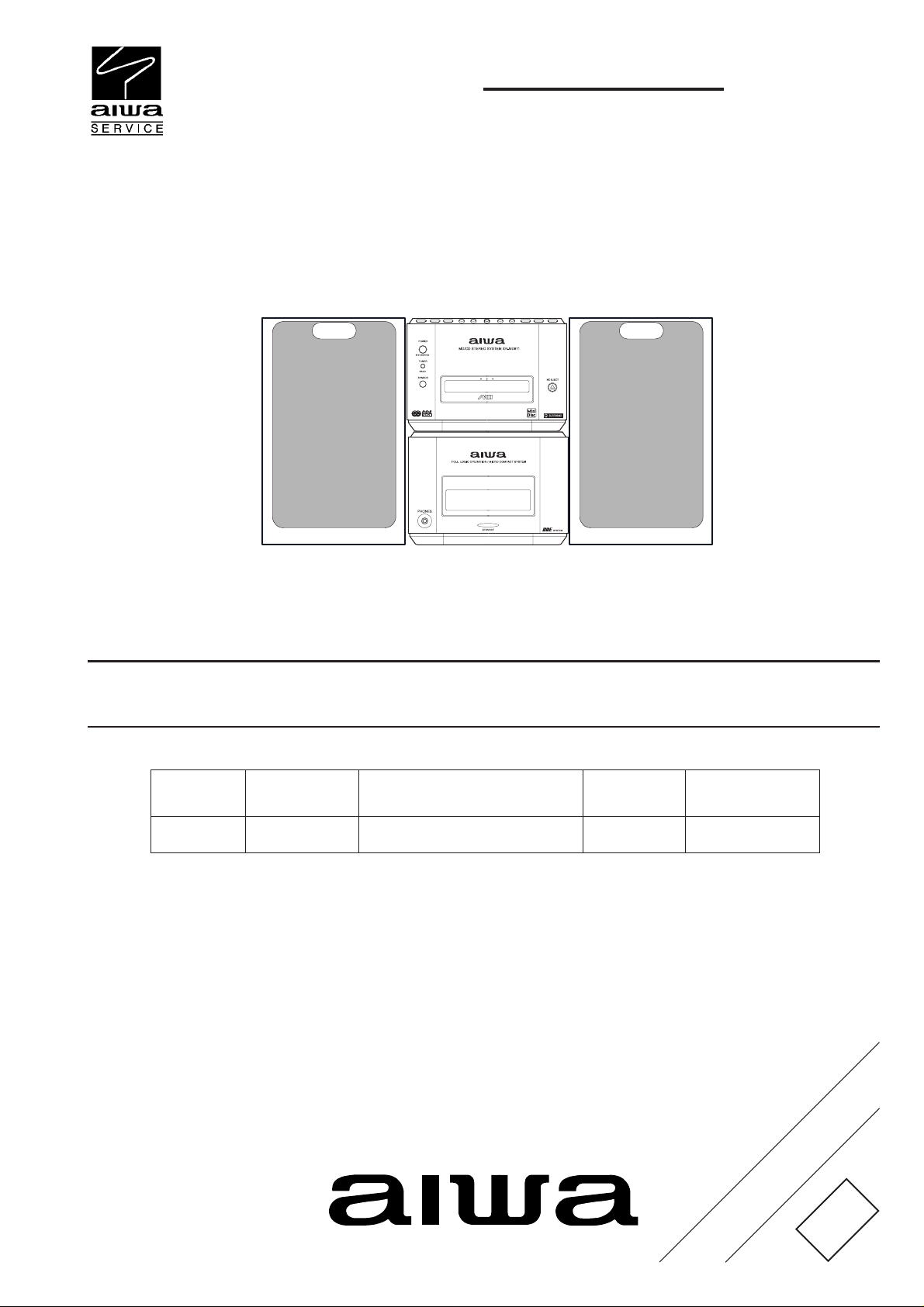
XR-MD811
EZ
SERVICE MANUAL
MD / CD
STEREO SYSTEM
SYSTEM
XR-MD811
• This Service Manual is the “Revision” and replaces “Simple Manual”
XR-MD811(EZ), (S/M Code No. 09-008-438-0T1).
• If requiring information about the MD mechanism, see Service Manual of
AZG-H, (S/M Code No. 09-005-346-5N2).
STEREO
RECEIVER
RX-LMD811
STEREO MD RECORD/
COMPACT DISC PLAYER
FM-LMD811
BASIC CD MECHANISM : DA23L
BASIC MD MECHANISM : AZG-H YA
SPEAKER
SX-LM810
REMOTE
CONTROLLER
RC-AAT21
S/M Code No. 09-00C-438-0R1
REVISION
DAT A
Page 2

TABLE OF CONTENTS
SPECIFICATIONS .................................................................................................................................................3
PROTECTION OF EYES FROM LASER BEAM DURING SERVICING ........................................................4
DISASSEMBLY INSTRUCTIONS....................................................................................................................5 ~ 6
MODEL NO. RX-LMD811
ELECTRICAL MAIN PARTS LIST ................................................................................................................7 ~ 9
TRANSISTOR ILLUSTRATION ..........................................................................................................................10
WIRING – 1 (POWER).........................................................................................................................................11
WIRING – 2 (PWR-AMP) .....................................................................................................................................12
WIRING – 3 (PT-MAIN / PT-SUB) .......................................................................................................................13
WIRING – 4 (TU-INF / JACK) ..............................................................................................................................14
SCHEMATIC DIAGRAM – 1 (POWER / PWR-AMP / PT-MAIN / PT-SUB / TU-INF / JACK).............................15
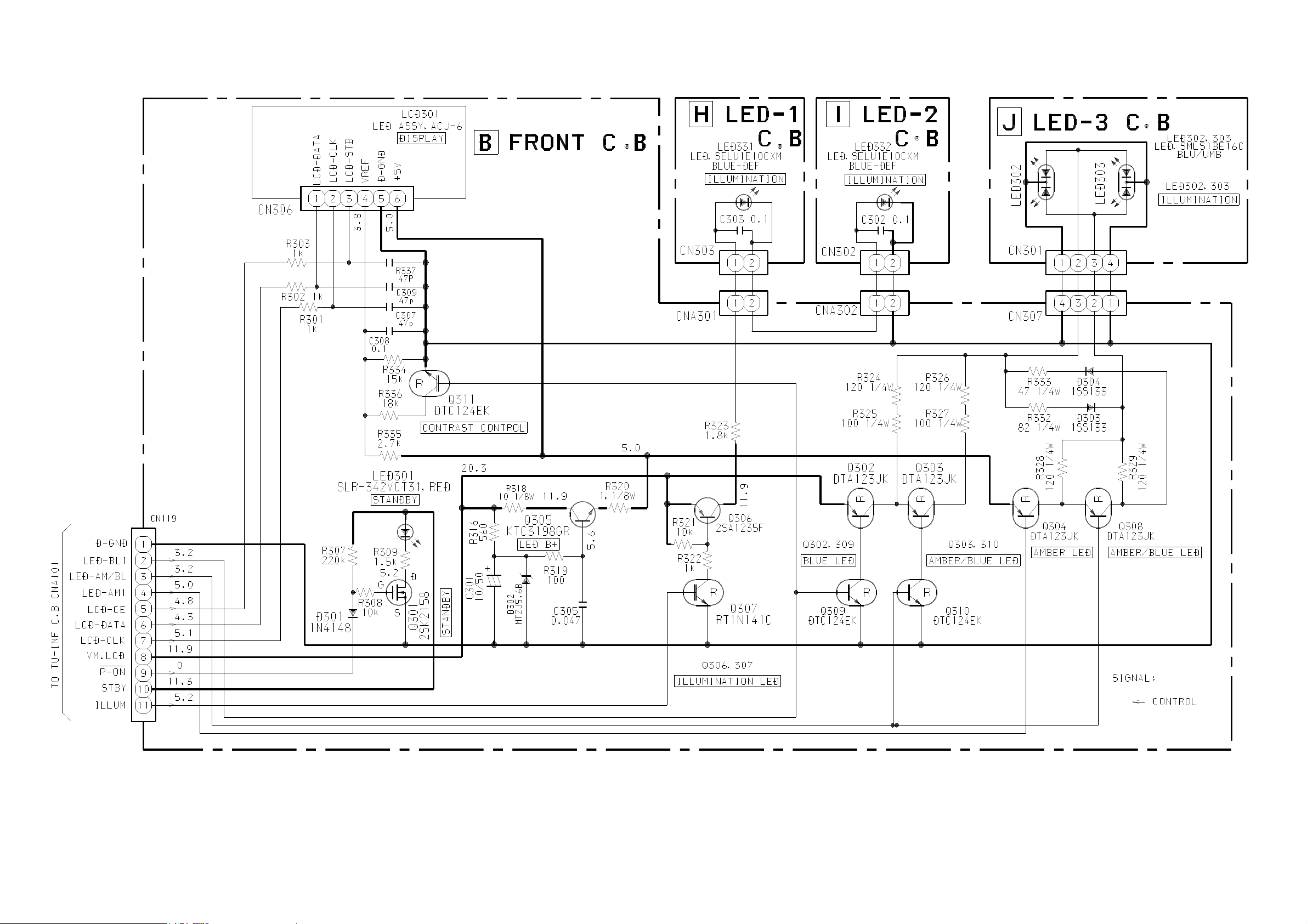
WIRING – 5 (FRONT / LED-1~3).........................................................................................................................16
SCHEMATIC DIAGRAM – 2 (FRONT / LED-1~3) ..............................................................................................17
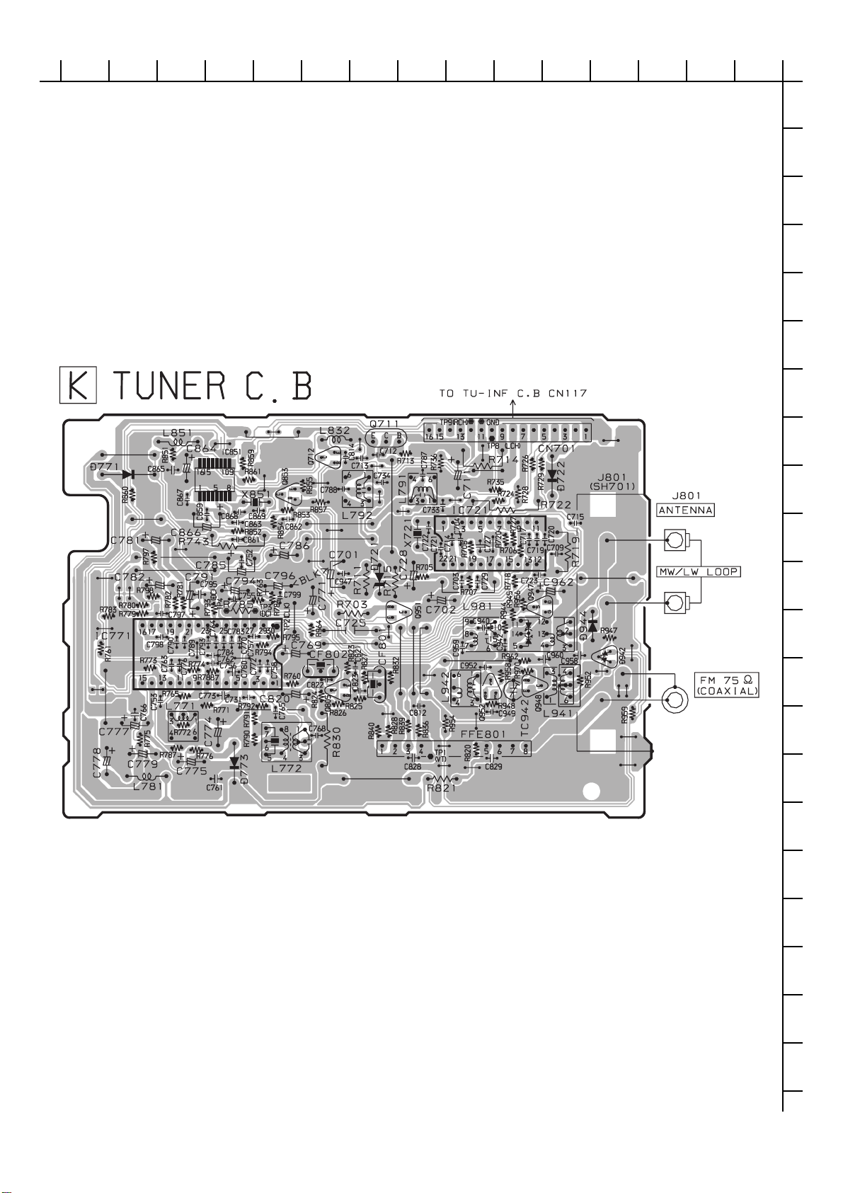
WIRING – 6 (TUNER) ..........................................................................................................................................18
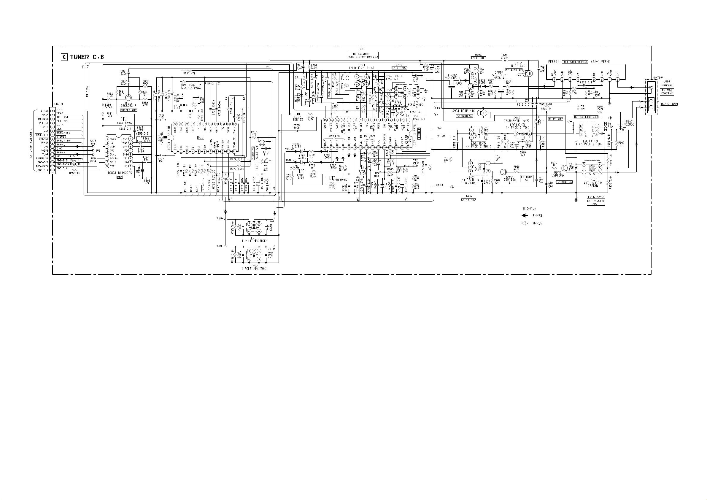
SCHEMATIC DIAGRAM – 3 (TUNER) ...............................................................................................................19
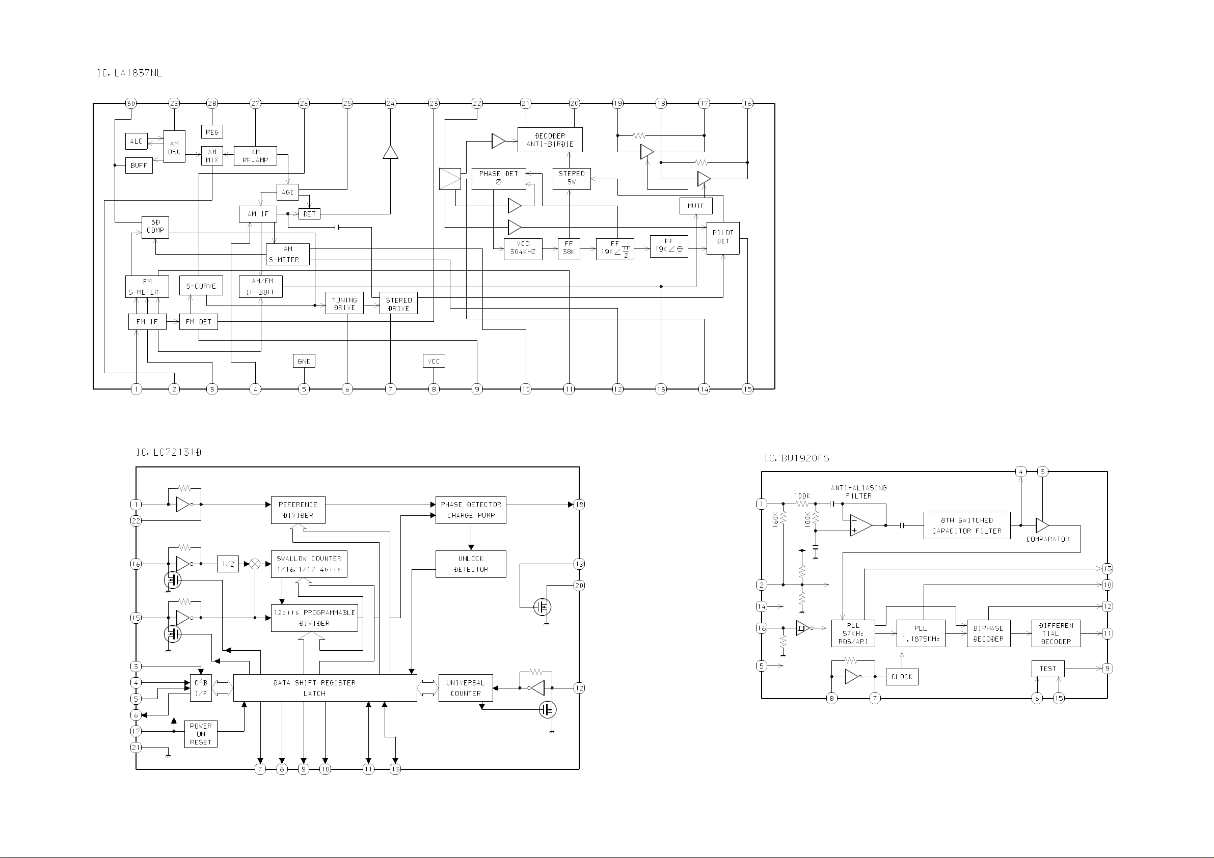
IC BLOCK DIAGRAM.........................................................................................................................................20
LCD DIAGRAM ....................................................................................................................................................21
ADJUSTMENT .....................................................................................................................................................22
MECHANICAL EXPLODED VIEW 1 / 1........................................................................................................... 23
MECHANICAL PARTS LIST 1 / 1 .....................................................................................................................24
MODEL NO. FM-LMD811
ELECTRICAL MAIN PARTS LIST ............................................................................................................25 ~ 27
TRANSISTOR ILLUSTRATION ..........................................................................................................................28
WIRING – 1 (FUNC / KEY / MOTOR / DOOR SW) .............................................................................................29
WIRING – 2 (FRONT / POWER / LED-L / LED-R) ..............................................................................................30
SCHEMATIC DIAGRAM – 1 (FUNC / FRONT / POWER / KEY / MOTOR / DOOR SW / LED-L / LED-R).......31
WIRING – 3 (CD) <1/2> .......................................................................................................................................32
WIRING – 3 (CD) <2/2> .......................................................................................................................................33
SCHEMATIC DIAGRAM – 2 (CD) <1/2> ............................................................................................................34
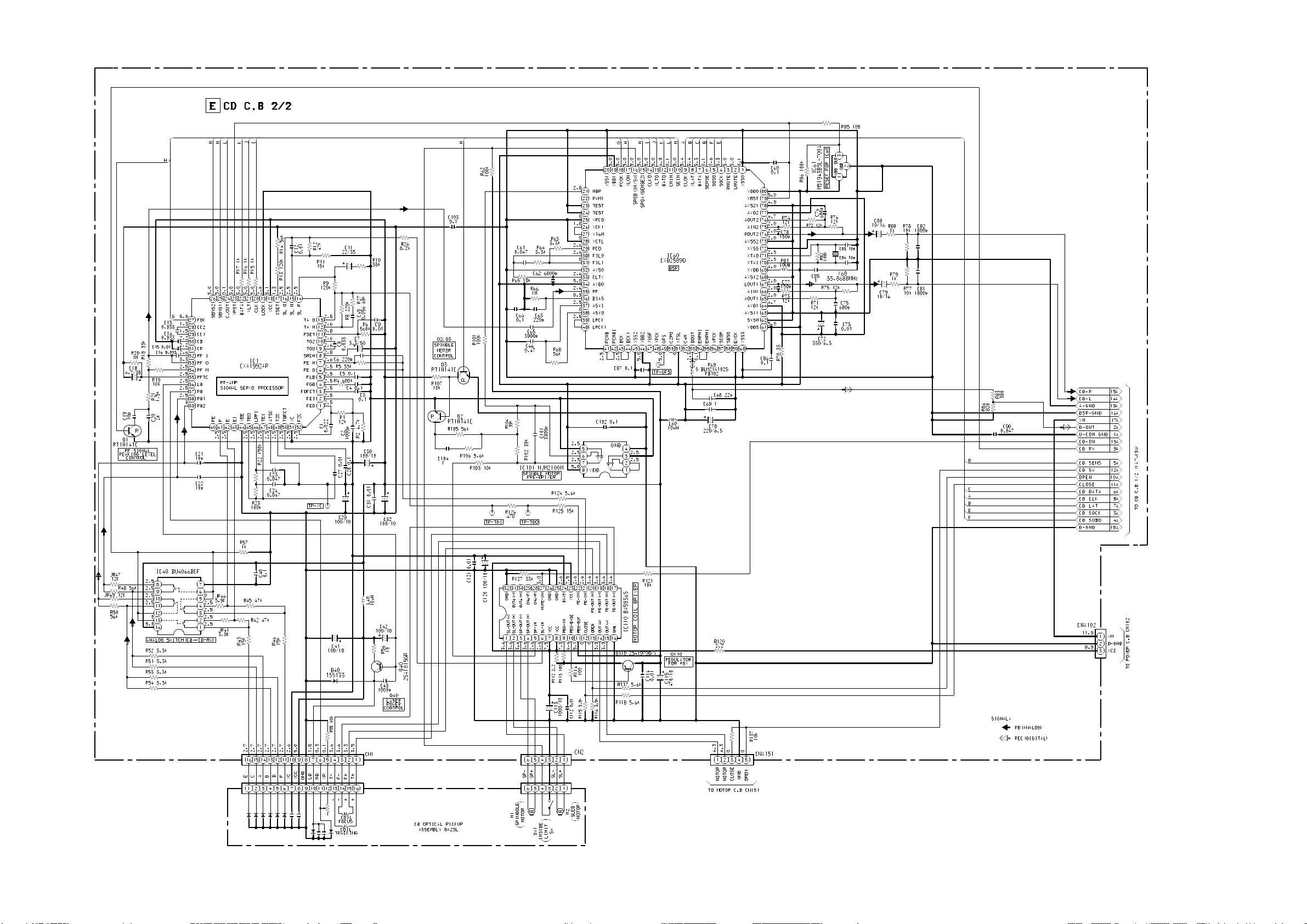
SCHEMATIC DIAGRAM – 3 (CD) <2/2> ............................................................................................................35
IC BLOCK DIAGRAM.........................................................................................................................................36
IC DESCRIPTION .......................................................................................................................................37 ~ 42
ADJUSTMENT <MD> ..................................................................................................................................43 ~ 51
CD TEST MODE ..................................................................................................................................................52
MD TEST MODE..........................................................................................................................................53 ~ 57
MECHANICAL EXPLODED VIEW 1 / 1............................................................................................................58
MECHANICAL PARTS LIST 1 / 1 .....................................................................................................................59
CD MECHANISM EXPLODED VIEW 1 / 1 ......................................................................................................60
CD MECHANISM PARTS LIST 1 / 1 ...............................................................................................................61
GENERAL SPEAKER DISASSEMBLY INSTRUCTIONS (FOR REFERENCE) .............................................62
SPEAKER PARTS LIST.....................................................................................................................................63
ACCESSORIES / PACKAGE LIST .....................................................................................................................63
– 2 –
Page 3

SPECIFICATIONS
STEREO RECEIVER RX-LMD811
<FM tuner section>
Tuning range 87.5 MHz to 108 MHz
Usable sensitivity (IHF) 16.8 dBf
Antenna terminals 75 ohms (unbalanced)
<MW tuner section>
Tuning range 531 kHz to 1602 kHz (9 kHz step)
530 kHz to 1710 kHz (10 kHz step)
Usable sensitivity 350 µV/m
Antenna Loop antenna
<LW tuner section>
Tuning range 144 kHz to 290 kHz
Usable sensitivity 1400 µV/m
Antenna Loop antenna
<Amplifier section>
Power output Rated : 16 W + 16 W (6 ohms,
T.H.D. 1 %, 1 kHz/DIN 45500)
Reference : 20 W + 20 W (6 ohms,
T.H.D. 10 %, 1 kHz/DIN 45324)
DIN MUSIC POWER
35 W + 35 W
Outputs SUPPER WOOFER : 1.0 V
SPEAKERS : accept speakers of
6 ohms or more
PHONES (stereo mini jack) : accepts
headphones of 32 ohms or more
<General>
Power requirements 230 V AC, 50 Hz
Power consumption 60 W
Standby power consumption
16 W (power economizing mode
deactivated)
1.7 W (power economizing mode
activated)
Dimensions of main unit 156 x 114 x 207 mm
(W x H x D)
Weight of main unit 2.8 kg
STEREO MD RECORDER / COMPACT DISC PLAYER
FM-LMD811
<MD recorder section>
Scanning method Non-contact optical scanner
(Semiconductor laser application)
Recording system Magnetic polarity modulation
overwrite system
Rotation speed Approx. 400 to 900 rpm (CLV)
Sampling frequency 44.1 kHz
No. of channels Stereo: 2 channels
Monaural: 1 channel
A-D, D-A converter 1-bit
Frequency 20 to 20000 Hz +0.5 - –1.5 dB
Wow and flatter Unmeasurable
General
Inputs TAPE IN : 500 mV
AUX IN : 500 mV
DIGITAL IN (OPTICAL) :
Outputs LINE OUT : 500 mV
Dimensions of main unit 156 x 114 x 200.7 mm
(W x H x D)
Weight of main unit 1.8 kg
SPEAKER SYSTEM SX-LM810
Cabinet type 2 way, bass reflex (magnetic
shielded type)
Speaker Woofer :
100 mm cone type
Tweeter :
22 mm dome type
Impedance 6 ohms
Output sound pressure level 86 dB/W/m
Dimensions 135 x 223 x 173 mm
(W x H x D)
Weight 1.8 kg
• Design and specifications are subject to change without notice.
• The word "BBE"and the "BBE symbol" are trademarks of BBE
Sound, Inc.
Under license from BBE Sound,Inc.
<Compact disc player section>
Laser Semiconductor laser (λ = 780 nm)
D-A converter 1 bit dual
Signal-to-noise ratio 85 dB (1 kHz, 0 dB)
Harmonic distortion 0.05 % (1 kHz, 0 dB)
Wow and flutter Unmeasurable
– 3 –
Page 4
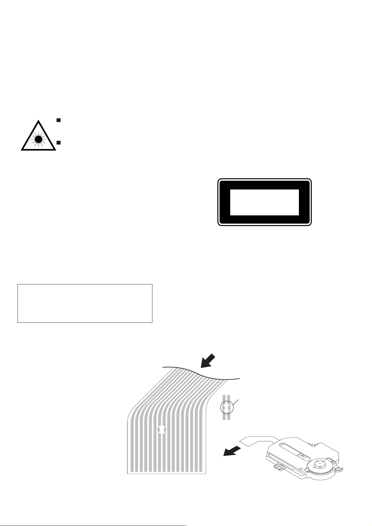
PROTECTION OF EYES FROM LASER BEAM DURING SERVICING
PICK UP ASSY
SF-P200L
:SOLDER
116
10 9
This set employs laser. Therefore, be sure to follow carefully the
instructions below when servicing.
WARNING!
WHEN SERVICING, DO NOT APPROACH THE LASER EXIT
WITH THE EYE TOO CLOSELY. IN CASE IT IS NECESSARY TO
CONFIRM LASER BEAM EMISSION. BE SURE TO OBSERVE
FROM A DISTANCE OF MORE THAN 30cm FROM THE
SURFACE OF THE OBJECTIVE LENS ON THE OPTICAL
PICK-UP BLOCK.
Caution: Invisible laser radiation when
open and interlocks defeated avoid exposure to beam.
Advarsel:Usynling laserståling ved åbning,
når sikkerhedsafbrydere er ude af funktion.
Undgå udsættelse for stråling.
VAROITUS!
Laiteen Käyttäminen muulla kuin tässä käyttöohjeessa mainitulla tavalla saattaa altistaa käyt-täjän turvallisuusluokan 1 ylittävälle näkymättömälle lasersäteilylle.
VARNING!
Om apparaten används på annat sätt än vad som specificeras i
denna bruksanvising, kan användaren utsättas för osynling
laserstrålning, som överskrider gränsen för laserklass 1.
CAUTION
Use of controls or adjustments or performance of procedures
other than those specified herein may result in hazardous
radiation exposure.
ATTENTION
L'utilisation de commandes, réglages ou procédures autres que
ceux spécifiés peut entraîner une dangereuse exposition aux
radiations.
ADVARSEL!
Usynlig laserståling ved åbning, når sikkerhedsafbrydereer ude
af funktion. Undgå udsættelse for stråling.
This Compact Disc player is classified as a CLASS 1 LASER
product.
The CLASS 1 LASER PRODUCT label is located on the rear
exterior.
CLASS 1
KLASSE 1
LUOKAN 1
KLASS 1
LASER PRODUCT
LASER PRODUKT
LASER LAITE
LASER APPARAT
Precaution to replace Optical block
(SF-P200L)
Body or clothes electrostatic potential could ruin
laser diode in the optical block. Be sure ground
body and workbench, and use care the clothes
do not touch the diode.
1) After the connection, remove solder shown in
the right figure.
– 4 –
Page 5
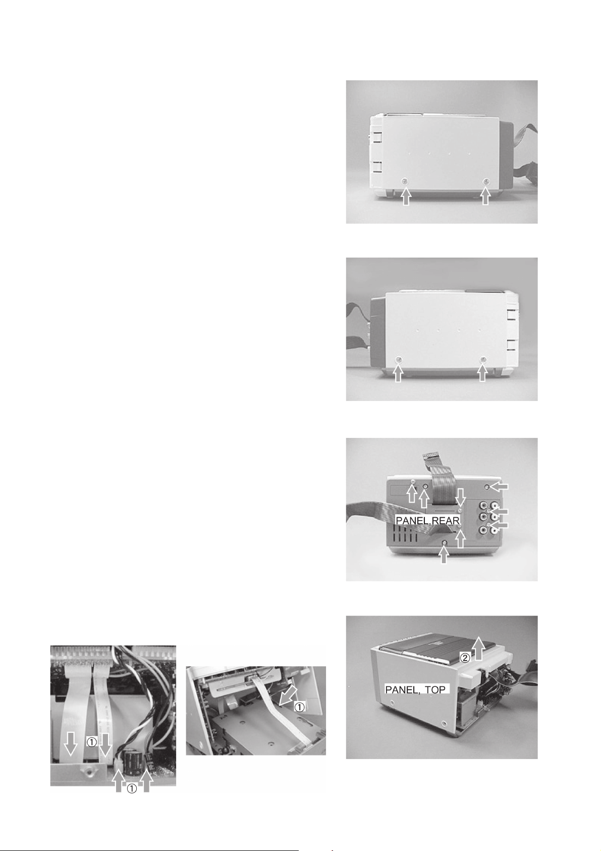
DISASSEMBLY INSTRUCTIONS
FM BLOCK DISASSEMBLY
1. Removing the Ornament Parts
1) Remove the two screws.
2) Remove the two screws.
3) Remove the eight screws and remove PANEL, REAR.
4) Remove the FFC from the connector 1 and remove PANEL,
TOP 2.
– 5 –
Page 6
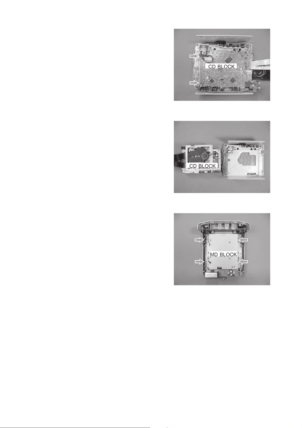
2. Removing the CD Block
1) Remove the two screws and remove the entire CD block.
2) The figure shows the states after the CD block is removed.
3. Removing the MD Block
1) Remove the four screws and remove the MD block.
– 6 –
Page 7

MODEL NO.
RX-LMD811
ELECTRICAL MAIN PARTS LIST
PART NO.
NO.
IC
87-070-127-110 IC,LC72131D
87-A20-913-010 IC,LA1837NL
87-A20-440-040 C-IC,BU1920FS
TRANSISTOR
89-213-702-010 TR,2SB1370E
87-026-610-080 TR,KTC3198GR
87-A30-076-080 C-TR,2SC3052F
87-A30-075-080 C-TR,2SA1235F
87-A30-234-080 TR,CSC4115BC
87-A30-083-080 TR,CSD1489B
87-A30-073-080 C-TR,RT1N 141C
87-A30-190-080 TR,CC5551
87-A30-109-010 TR,2SD 2495
87-A30-108-010 TR,2SB1626
87-A30-119-040 C-TR,2SC3906K R
87-A30-047-080 TR,CSD655E
87-026-609-080 TR,KTA1266GR
87-A30-107-070 C-TR,CMBT5401
87-A30-074-080 C-TR,RT1P 141C
87-A30-087-080 C-FET,2SK2158
87-026-580-080 C-TR,DTA123JK
87-026-236-080 C-TR,DTC124EK
89-505-434-540 C-FET,2SK543-TB(4/5)
89-327-143-080 C-TR,2SC2714(0.1W)
87-A30-072-080 C-TR,RT1P 144C
87-A30-086-070 C-TR,CSD1306E
DIODE
87-070-345-080 DIODE,IN4148
87-070-178-090 DIODE,1N5402-BD54
87-070-274-080 DIODE,1N4003 SEM
87-A40-345-080 ZENER,MTZJ10C
87-A40-269-080 C-DIODE,MC2836
87-A40-270-080 C-DIODE,MC2838
87-A40-004-080 ZENER,MTZJ16A
87-A40-313-080 C-DIODE,MC 2840
87-A40-488-080 DIODE,1SS244
87-017-931-080 ZENER,MTZJ5.6B
87-020-465-080 DIODE,1SS133
87-017-149-080 ZENER,HZS6A2L
POWER C.B
C102 87-016-051-090 CAP,E 2200-35 M SMG
C103 87-016-051-090 CAP,E 2200-35 M SMG
C106 87-010-196-080 CHIP CAPACITOR,0.1-25
C107 87-010-196-080 CHIP CAPACITOR,0.1-25
C108 87-010-196-080 CHIP CAPACITOR,0.1-25
C109 87-010-196-080 CHIP CAPACITOR,0.1-25
C110 87-010-388-010 CAP, E 1000-25 SME
C111 87-012-140-080 C-CAP,S 470P-50
C113 87-010-247-080 CAP, ELECT 100-50V
C114 87-010-112-080 CAP, ELECT 100-16V
C115 87-010-235-080 CAP,E 470-16 SME
C132 87-010-260-080 CAP, ELECT 47-25V
C133 87-010-403-080 CAP, ELECT 3.3-50 M 11L SME
C135 87-010-381-080 CAP, ELECT 330-16V
C136 87-010-101-080 CAP, ELECT 220-16
C137 87-010-235-080 CAP,E 470-16 SME
C151 87-010-196-080 C-CAP,S 0.1-25 Z F
C152 87-A11-174-090 CAP,E 4700-16 M SMG
DESCRIPTIONREF. NO. KANRI
PART NO.
NO.
C219 87-010-184-080 CHIP CAPACITOR 3300P-50
C220 87-010-184-080 CHIP CAPACITOR 3300P-50
C281 87-010-401-080 CAP, ELECT 1-50V
C282 87-010-263-080 CAP, ELECT 100-10V
C283 87-010-380-080 CAP, ELECT 47-16V
C284 87-010-260-080 CAP, ELECT 47-25V
CN101 87-A60-813-010 CONN,8P H BLK TAC-L8P
CN102 87-A60-813-010 CONN,8P H BLK TAC-L8P
CN115 87-A60-624-010 CONN,7P V 2MM JMT
CN203 87-A60-109-010 CONN,2P V S2M-2W
J201 87-A60-420-010 JACK,3.5 ST (MSC)
J202 87-099-801-010 JACK,PIN 1P BLK W/O SW
J501 87-009-065-010 CONNECTOR, 15P H FG
WH104 87-A90-507-010 HLDR,WIRE 2.5-4P
FRONT C.B
C301 87-010-405-080 CAP, ELECT 10-50V
C305 87-010-194-080 CAP, CHIP 0.047
C307 87-010-318-080 C-CAP,S 47P-50 CH
C308 87-A11-144-080 CAP,TC U 0.1-50 KB
C309 87-018-115-080 CAP,TC U 47P-50
CN119 87-A60-675-010 CONN,11P H 2MM JMT
CN306 87-A60-899-010 CONN,6P V BLK FMN-BTRK
CN307 87-099-564-010 CONN,4P TUC-P4P-B1
CNA301 88-805-020-790 CONN ASSY,2P 70MM
CNA302 88-805-020-790 CONN ASSY,2P 70MM
LCD301 8A-CJ6-620-010 LCD ASSY,ACJ-6
LED301 87-A40-317-080 LED,SLR-342VCT31 RED
R337 87-010-318-080 C-CAP,S 47P-50 CH
PWR-AMP C.B
C201 87-010-260-080 CAP, ELECT 47-25V
C202 87-010-260-080 CAP, ELECT 47-25V
C203 87-A10-946-080 C-CAP,S 220P-100 J CH
C204 87-A10-946-080 C-CAP,S 220P-100 J CH
C209 87-010-186-080 CAP,CHIP 4700P
C210 87-010-186-080 CAP,CHIP 4700P
C211 87-012-368-080 C-CAP,S 0.1-50 F
C212 87-012-368-080 C-CAP,S 0.1-50 F
C213 87-010-195-080 C-CAP,S 0.068-25 F
C214 87-010-195-080 C-CAP,S 0.068-25 F
C215 87-010-544-080 CAP, ELECT 0.1-50V
C216 87-010-544-080 CAP, ELECT 0.1-50V
C217 87-010-182-080 C-CAP,S 2200P-50 B
C218 87-010-182-080 C-CAP,S 2200P-50 B
C221 87-010-186-080 CAP,CHIP 4700P
C222 87-010-186-080 CAP,CHIP 4700P
C223 87-010-403-080 CAP,E 3.3-50 M 11L
C224 87-010-403-080 CAP,E 3.3-50 M 11L
C225 87-012-157-080 C-CAP,S 330P-50 CH
C226 87-012-157-080 C-CAP,S 330P-50 CH
C265 87-010-546-080 CAP,E 0.33-50 11L
C266 87-010-546-080 CAP,E 0.33-50 11L
C271 87-015-819-080 CAPACITOR,0.01
C277 87-010-197-080 CAP, CHIP 0.01 DM
CN201 87-A60-812-010 CONN,8P V BLK TAC-L8P
CN202 87-A60-812-010 CONN,8P V BLK TAC-L8P
J203 87-YP6-608-010 TERMINAL,SPKR 4P
L201 87-003-383-010 COIL,1UHK
L202 87-003-383-010 COIL,1UHK
R215 87-A00-258-080 RES,M/F 0.22-1W J
R216 87-A00-258-080 RES,M/F 0.22-1W J
R217 87-A00-258-080 RES,M/F 0.22-1W J
DESCRIPTIONREF. NO. KANRI
– 7 –
Page 8

PART NO. DESCRIPTIONREF. NO. KANRI
DESCRIPTIONREF. NO. KANRI
NO.
R218 87-A00-258-080 RES,M/F 0.22-1W J
R219 87-A00-258-080 RES,M/F 0.22-1W J
R220 87-A00-258-080 RES,M/F 0.22-1W J
TH201 87-A91-042-080 C-THMS,100K 55001
TH202 87-A91-042-080 C-THMS,100K 55001
PT-MAIN C.B
C155 87-010-196-080 CHIP CAPACITOR,0.1-25
C191 87-A10-479-080 CAP,CER 2200P-250 M E KH
!
PR151 87-A90-094-080 PROTECTOR,4A 491SERIES 60V
!
PT101 8Z-CL1-623-010 PT,E
!
RY102 87-A90-976-010 RELAY,AC12V SDT-S-112LMR
!
T101 87-A60-317-010 TERMINAL, 1P MSC
!
T102 87-A60-317-010 TERMINAL, 1P MSC
W101 8A-CU2-662-010 F-CABLE,5P 2.5MM 150MM
W102 8Z-CL1-654-010 F-CABLE,2P 2.5 170MM SUBPT
W103 8Z-CL1-655-010 F-CABLE,4P 2.5 100MM PWR
WH101 87-A90-459-010 HLDR,WIRE 2.5-5P
WH103 87-A90-507-010 HLDR,WIRE 2.5-4P
WH112 87-A90-506-010 HLDR,WIRE 2.5-2P
PT-SUB C.B
C101 87-A10-831-080 CAP,E 1000-25 M SMG
C195 87-010-403-080 CAP, ELECT 3.3-50V
!
PT102 8Z-NF8-659-010 PT,SUB ZNF-8(E)TAM
WH111 87-A90-506-010 HLDR,WIRE 2.5-2P
TU-INF C.B
C504 87-010-190-080 CHIP CAPACITOR,0.01-25
CN116 87-099-574-010 CONN,20P TUC-P20P-B1
CN117 87-A60-189-010 CONN,16P V TUC-P16P-B1
CNA101 8A-CU2-660-010 CONN ASSY,11P 2MM
CNA303 8A-CU2-661-010 CONN ASSY,7P 2MM
JACK C.B
C182 87-010-322-080 C-CAP,S 100P-50 CH
C183 87-010-322-080 C-CAP,S 100P-50 CH
C184 87-010-322-080 C-CAP,S 100P-50 CH
C185 87-010-322-080 C-CAP,S 100P-50 CH
C186 87-010-322-080 C-CAP,S 100P-50 CH
C187 87-010-322-080 C-CAP,S 100P-50 CH
CN104 87-099-563-010 CONN,20P TUC-P20X-B1
J502 87-A60-782-010 CONN,19P H FG
LED-1 C.B
C303 87-A11-148-080 CAP,TC U 0.1-50
CN303 87-A60-619-010 CONN,2P V 2MM JMT
LED331 87-A40-678-010 LED,SELU1E10CXM BLUE-DEF
LED-2 C.B
C302 87-A11-148-080 CAP,TC U 0.1-50
CN302 87-A60-619-010 CONN,2P V 2MM JMT
LED332 87-A40-678-010 LED,SELU1E10CXM BLUE-DEF
LED-3 C.B
CN301 87-099-553-010 CONN,4P H TUC-P
LED302 87-A40-821-080 LED,SMLS1BE16C BLU/UMB
LED303 87-A40-821-080 LED,SMLS1BE16C BLU/UMB
TUNER C.B
C701 87-010-381-080 CAP,ELECT 330-16V
C702 87-010-404-080 CAP,ELECT 4.7-50V
C703 87-012-286-080 CAP,U 0.01-25
C704 87-012-286-080 CAP,U 0.01-25
PART NO.
NO.
C709 87-012-195-080 C-CAP,U 100P-50CH
C711 87-010-260-080 CAP,ELECT 47-25V
C712 87-010-831-080 C-CAP,U,0.1-16F
C713 87-012-286-080 CAP,U 0.01-25
C714 87-012-286-080 CAP,U 0.01-25
C715 87-012-195-080 C-CAP,U 100P-50CH
C717 87-012-286-080 CAP,U 0.01-25
C719 87-012-286-080 CAP,U 0.01-25
C720 87-012-195-080 C-CAP,U 100P-50CH
C721 87-012-176-080 CAP,15P
C722 87-012-176-080 CAP,15P
C723 87-012-274-080 CHIP CAP,U 1000P-50B
C727 87-010-196-080 CHIP CAPACITOR,0.1-25
C728 87-010-248-080 CAP,ELECT 220-10V
C729 87-012-274-080 CHIP CAP,U 1000P-50B
C731 87-012-286-080 CAP,U 0.01-25
C733 87-012-280-080 C-CAP,U 3300P-50 KB
C734 87-012-280-080 C-CAP,U 3300P-50 KB
C752 87-012-282-080 C-CAP,U 4700P-50 KB
C753 87-012-195-080 C-CAP,U 100P-50 J CH
C755 87-012-286-080 CAP,U 0.01-25
C756 87-012-286-080 CAP,U 0.01-25
C757 87-012-188-080 C-CAP,U 47P-50 CH
C758 87-012-167-080 C-CAP,U 5P-50 CH
C761 87-010-196-080 C-CAP,S 0.1-25 ZF
C762 87-012-286-080 CAP,U 0.01-25
C763 87-010-829-080 CAP,U 0.047-16
C764 87-012-145-080 C-CAP,S 270P-50 J CH
C765 87-012-286-080 CAP,U 0.01-25
C766 87-010-197-080 C-CAP,S 0.01-25 KB
C768 87-012-286-080 CAP,U 0.01-25
C769 87-010-260-080 CAP,ELECT 47-25V
C770 87-010-829-080 CAP,U 0.047-16
C771 87-010-383-080 CAP,ELECT 33-25V
C772 87-010-829-080 CAP,U 0.047-16
C773 87-010-196-080 CHIP CAPACITOR,0.1-25
C774 87-010-263-080 CAP,ELECT 100-10V
C775 87-010-404-080 CAP,ELECT 4.7-50V
C776 87-012-286-080 CAP,U 0.01-25
C777 87-010-493-080 CAP,E 0.47-50 M 5L SRE
C778 87-010-401-080 CAP,ELECT 1-50V
C779 87-010-401-080 CAP,ELECT 1-50V
C780 87-010-196-080 CHIP CAPACITOR,0.1-25
C781 87-010-405-080 CAP,ELECT 10-50V
C782 87-010-405-080 CAP,ELECT 10-50V
C783 87-012-286-080 CAP,U 0.01-25
C784 87-012-286-080 CAP,U 0.01-25
C785 87-010-402-080 CAP,ELECT 2.2-50V
C786 87-010-402-080 CAP,ELECT 2.2-50V
C787 87-012-275-080 C-CAP,U 1200P-50 B
C788 87-012-275-080 C-CAP,U 1200P-50 B
C789 87-012-275-080 C-CAP,U 1200P-50 B
C790 87-012-275-080 C-CAP,U 1200P-50 B
C791 87-010-405-080 CAP,ELECT 10-50V
C793 87-012-273-080 C-CAP,U 820P-50 B
C794 87-010-406-080 CAP,ELECT 22-50
C795 87-010-596-080 CAP,S 0.047-16
C796 87-010-403-080 CAP,ELECT 3.3-50V
C797 87-012-276-080 C-CAP,U 1500P-50 KB
C798 87-012-276-080 C-CAP,U 1500P-50 KB
C799 87-010-829-080 CAP,U 0.047-16
C812 87-012-286-080 CAP,U 0.01-25
C814 87-012-286-080 CAP,U 0.01-25
C820 87-010-260-080 CAP,ELECT 47-25V
C821 87-012-286-080 CAP,U 0.01-25
C822 87-012-286-080 CAP,U 0.01-25
C823 87-012-286-080 CAP,U 0.01-25
C828 87-010-196-080 CHIP CAPACITOR,0.1-25
C829 87-010-196-080 CHIP CAPACITOR,0.1-25
C859 87-012-286-080 C-CAP,U 0.01-25 KB
– 8 –
Page 9
PART NO. DESCRIPTIONREF. NO. KANRI
NO.
C861 87-012-199-080 C-CAP,U 220P-50 J CH
C862 87-012-199-080 C-CAP,U 220P-50 J CH
C863 87-012-270-080 C-CAP,U 470P-50 KB
C864 87-010-405-080 CAP,E 10-50 M 11L SME
C865 87-010-196-080 C-CAP,S 0.1-25 ZF
C866 87-010-405-080 CAP,E 10-50 M 11L SME
C867 87-012-286-080 C-CAP,U 0.01-25 KB
C868 87-012-184-080 C-CAP,U 33P-50 J CH
C869 87-012-180-080 C-CAP,U 22P-50 J CH
C940 87-012-286-080 C-CAP,U 0.01-25 KB
C942 87-012-168-080 C-CAP,U 6P-50 D CH
C947 87-012-286-080 C-CAP,U 0.01-25 KB
C949 87-A10-039-080 C-CAP,U 470P-50 J CH
C952 87-012-286-080 C-CAP,U 0.01-25 KB
C958 87-010-197-080 C-CAP,S 0.01-25 KB
C959 87-010-831-080 C-CAP,U 0.1-16 ZF
C960 87-010-196-080 CHIP CAPACITOR,0.1-25
C962 87-010-401-080 CAP,E 1-50 M 11L SME
CF801 87-008-423-010 FLTR,CF SFE10.7MS3G-A
CF802 82-785-747-010 CF,MS2 GHY R
DESCRIPTIONREF. NO. KANRI
PART NO.
NO.
CN701 87-A60-650-010 CONN,16P H GRY TUC-P16X-C1
FFE801 A8-6ZA-191-130 6ZA-1 FEENM
J801 87-033-241-010 TERMINAL,ANT 2P AJ-2039
L771 87-A50-266-010 COIL,FM DET-2N(TOK)
L772 87-A91-110-010 FLTR,PCFJZH-450(TOK)
L781 87-005-847-080 COIL,2.2UH CECS
L791 87-A50-027-010 COIL,1 POLE MPX(TOK)
L792 87-A50-027-010 COIL,1 POLE MPX(TOK)
L832 87-005-847-080 COIL,2.2UH K CECS
L851 87-005-847-080 COIL,2.2UH K CECS
L941 87-A50-020-010 COIL,ANT LW(COI)252KHZ
L942 87-A50-019-010 COIL,OSC LW(COI) 856KHZ
L981 8Z-ZA1-665-010 COIL,AM PACK 2(TOK)
TC942 87-011-164-010 TRIMMER,CER 30P 4.5X3.9 VCT31
X721 87-A70-061-010 VIB,XTAL 4.500MHZ CSA-309
X851 87-A70-091-010 VIB,XTAL 4.332MHZ CSA-309
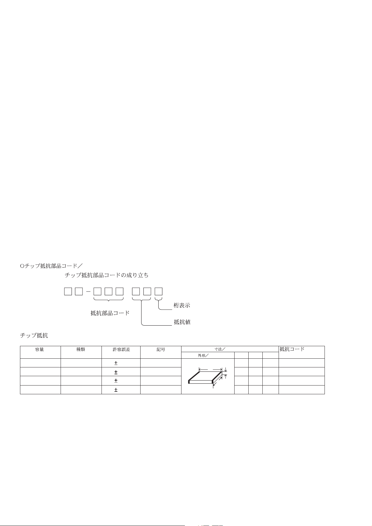
CHIP RESISTOR PART CODE
Chip Resistor Part Coding
88
A
Resistor Code
Chip resistor
Wattage Type Tolerance
1/16W 1005 5% CJ
1/16W
1/10W
1/8W
1608
2125
3216
5%
5%
5%
Symbol
CJ
CJ
CJ
Figure
Value of resistor
Form
L
Dimensions (mm)
t
W
0.55
Resistor Code
108
118
128
LW t
1.0 0.5 0.35 104
1.6 0.8 0.45
2 1.25 0.45
3.2
1.6
: A
: A
– 9 –
Page 10
TRANSISTOR ILLUSTRATION
E C B
CSD655
KTA1266
KTC3198
B C E
2SD2495
2SB1626
E C B
CSC4115
G
S
2SK2158
B C E
2SB1370
E C B
CSD1489
CC5551
D
G
D
2SK543
S
B
2SA1235
2SC2714
2SC3052
2SC3906
CMBT5401
C
E
DTA123JK
DTC124EK
RT1N141C
RT1P141C
RT1P144C
CSD1306
– 10 –
Page 11
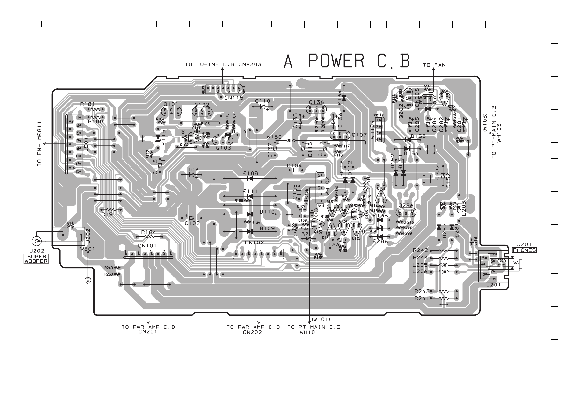
WIRING 1 (POWER)
32 31 30 29 28 27 26 25 24 23 22 21 20 19 18 17 16 15 14 13 12 11 10 9 8 7 6 5 4 3 2 1
A
B
C
D
E
F
G
H
I
J
K
L
M
N
O
P
Q
11
R
S
T
U
Page 12
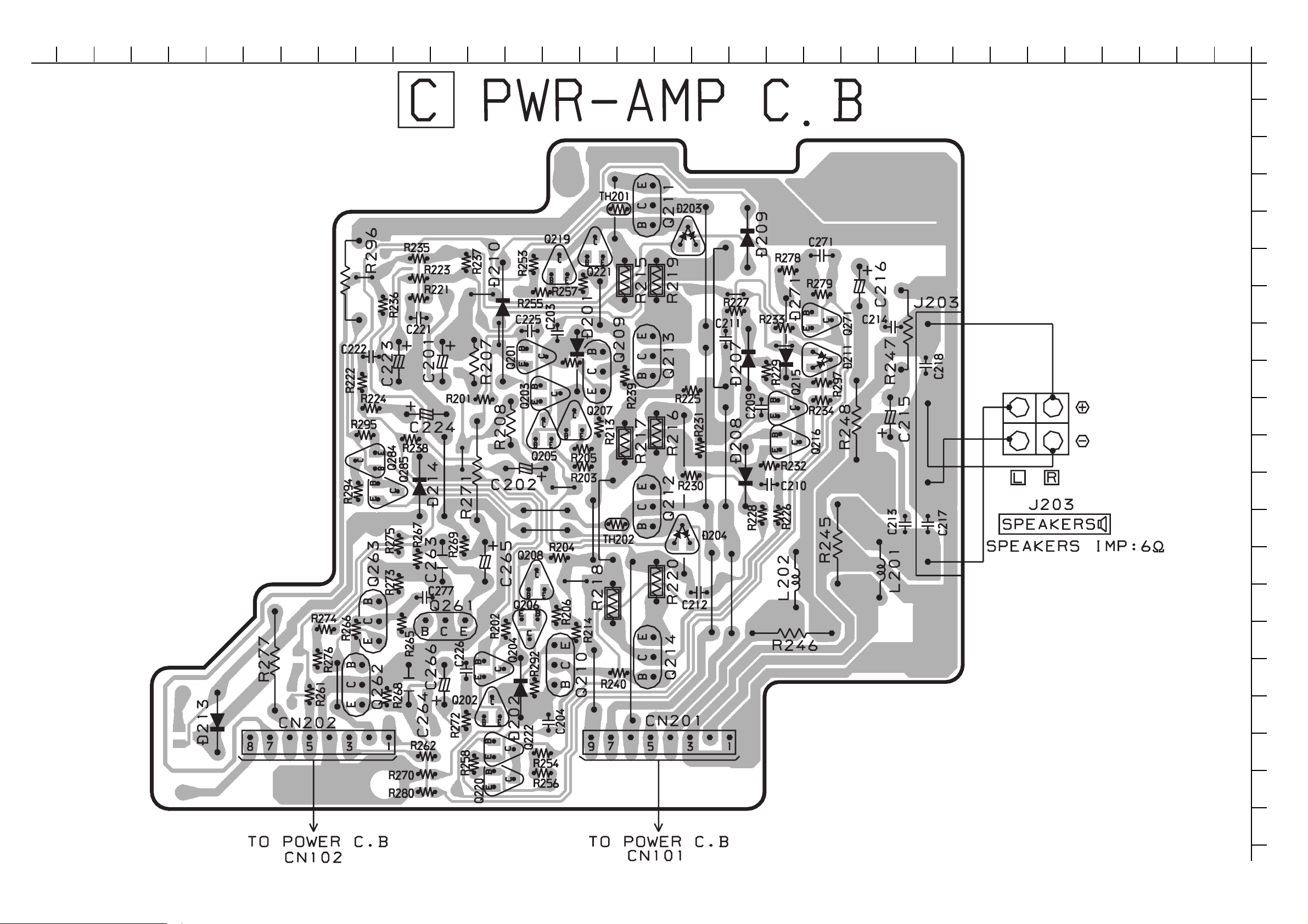
WIRING – 2 (PWR – AMP)
32 31 30 29 28 27 26 25 24 23 22 21 20 19 18 17 16 15 14 13 12 11 10 9 8 7 6 5 4 3 2 1
A
B
C
D
E
F
G
H
I
J
K
L
M
N
O
P
Q
– 12 –
R
S
T
U
Page 13
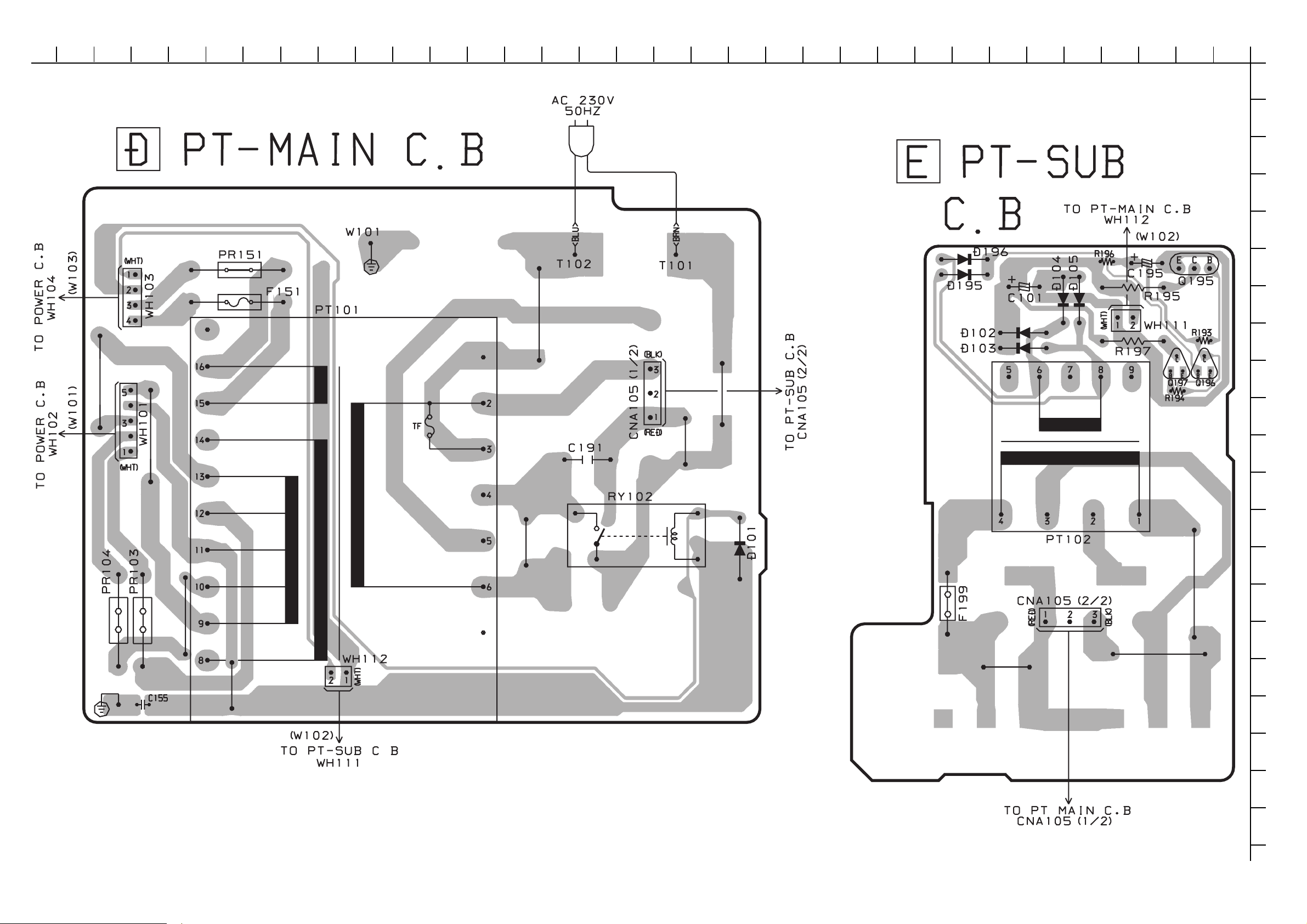
WIRING – 3 (PT – MAIN / PT – SUB)
32 31 30 29 28 27 26 25 24 23 22 21 20 19 18 17 16 15 14 13 12 11 10 9 8 7 6 5 4 3 2 1
A
B
C
D
E
F
G
H
I
J
K
L
M
N
O
P
Q
– 13 –
R
S
T
U
Page 14
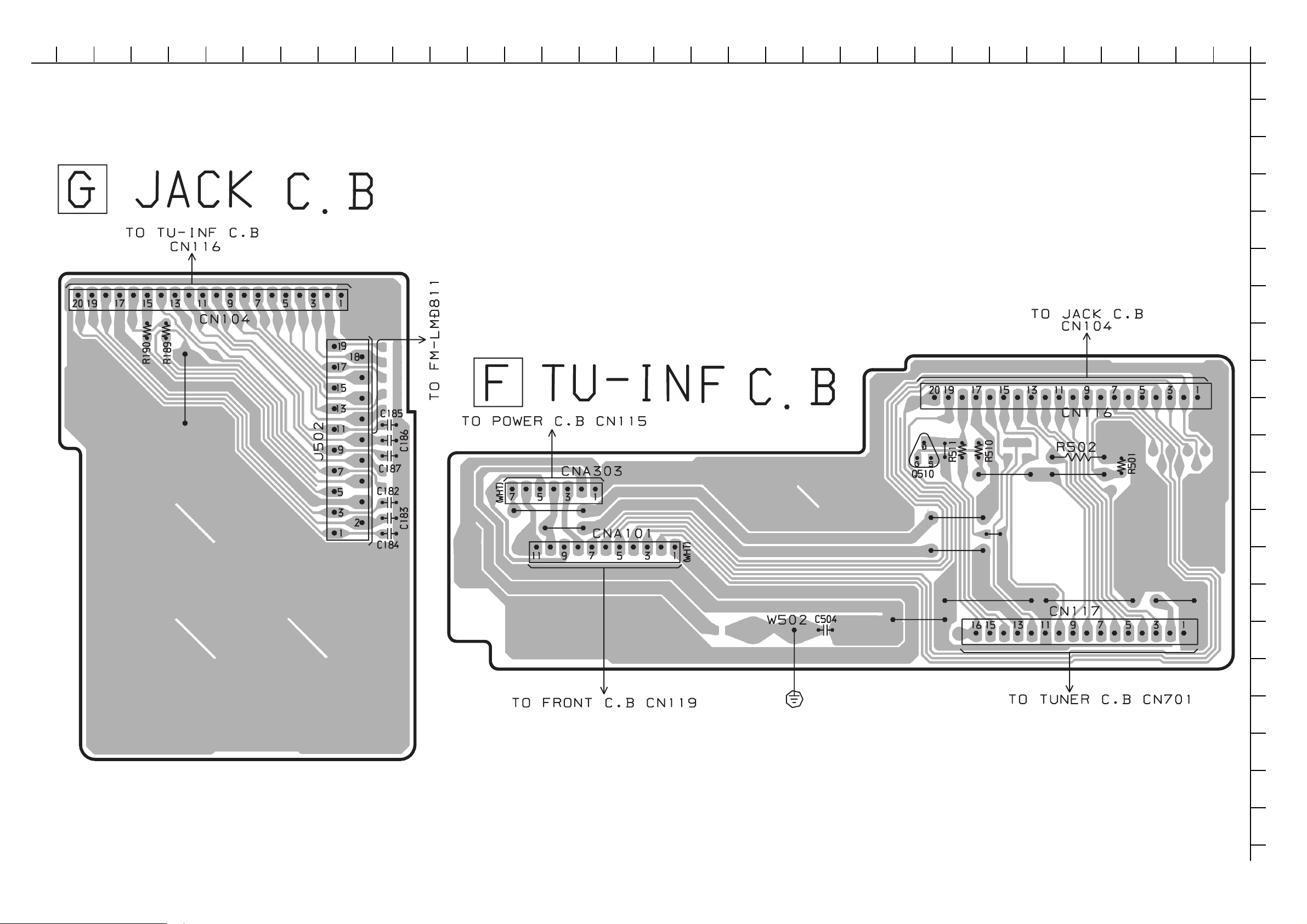
WIRING 4 (TU INF / JACK)
32 31 30 29 28 27 26 25 24 23 22 21 20 19 18 17 16 15 14 13 12 11 10 9 8 7 6 5 4 3 2 1
A
B
C
D
E
F
G
H
I
J
K
L
M
N
O
P
Q
14
R
S
T
U
Page 15
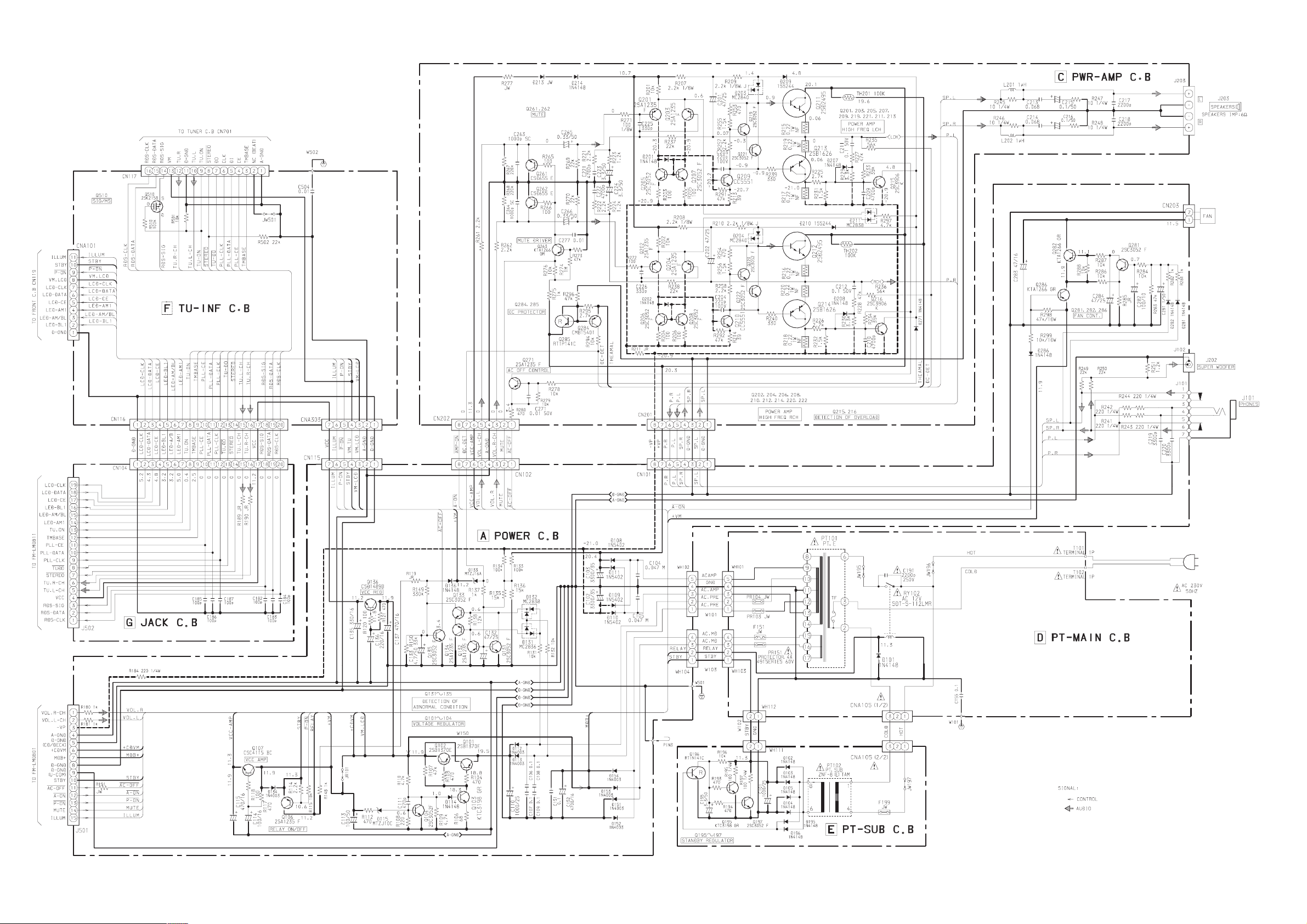
SCHEMATIC DIAGRAM 1 (POWER / PWR-AMP / PT-MAIN / PT-SUB / TU-INF / JACK)
15
Page 16
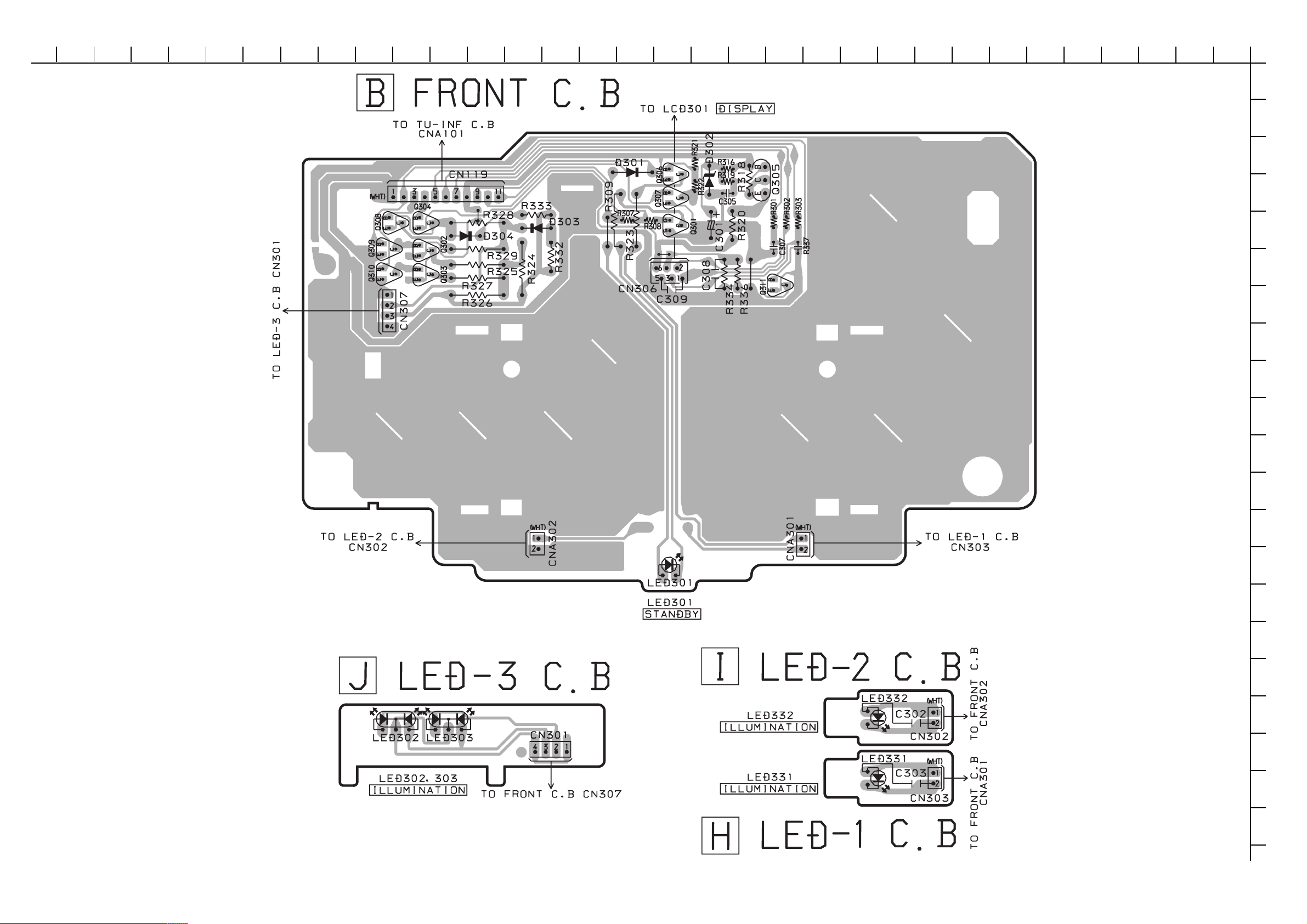
WIRING – 5 (FRONT / LED 1 ~ 3)
32 31 30 29 28 27 26 25 24 23 22 21 20 19 18 17 16 15 14 13 12 11 10 9 8 7 6 5 4 3 2 1
A
B
C
D
E
F
G
H
I
J
K
L
M
N
O
P
Q
– 16 –
R
S
T
U
Page 17
SCHEMATIC DIAGRAM – 2 (FRONT / LED-1 / LED-2 / LED-3)
– 17 –
Page 18
WIRING – 6 (TUNER)
15 14 13 12 11 10 9 8 7 6 5 4 3 2 1
A
B
C
D
E
F
G
H
I
J
K
L
M
N
O
P
Q
– 18 –
R
S
T
U
Page 19
SCHEMATIC DIAGRAM – 3 (TUNER)
– 19 –
Page 20
IC BLOCK DIAGRAM
– 20 –
Page 21

LCD DIAGRAM
LCD ASSY, ACJ-6
– 21 –
Page 22

ADJUSTMENT
TUNER SECTION
1. Clock Frequency Check
Settings : • Test point : TP2 (CLK)
Method : Set to MW 1602kHz and check that the test
point is 2052kHz ± 45Hz.
6. AM IF Adjustment
Settings : • Test point : TP8 (Lch), TP9 (Rch)
• Adjustment location :
L772 ........................... 450kHz
2. MW VT Check
Settings : • Test point : TP1 (VT)
Method : Set to MW 1602kHz and check that the test point is
less than 8.0V. Then set to MW 531kHz and check
that the test point is more than 0.6V.
3. MW Tracking Adjustment
Settings : • Test point : TP8 (Lch), TP9 (Rch)
• Adjustment location : L981 (1/3)
Method : Set to MW 999kHz and adjust L981 (1/3) so
that the test point becomes maximum.
4. LW VT Adjustment
Settings : • Test point : TP1 (VT)
• Adjustment location : L942
Method : Set to LW 144kHz and adjust L942 so that the test
point becomes 1.3V ± 0.05V.
Then set to LW 290kHz and check that the test point is
less than 8.0V.
5. LW Tracking Adjustment
Settings : • Test point : TP8 (Lch), TP9 (Rch)
• Adjustment location :
L941 ........................... 144kHz
TC942 ......................... 290kHz
Method : Set up TC942 to center before adjustment.
The level at 144kHz is adjusted to maximum by L941.
Then the level at 290kHz is adjusted
to maximum by TC942.
7. FM VT Check
Settings : • Test point : TP1 (VT)
Method : Set to FM 108.0MHz and check that the test
point is less than 8.0V. Then set to FM
87.5 MHz and check that the test point is more
than 0.5V.
8. FM Tracking Check
Settings : • Test point : TP8 (Lch), TP9 (Rch)
Method : Set to FM 98.0MHz and check that the test
point is less than 13dBµV.
9. DC Balance / Mono Distortion Adjustment
Settings : • Test point : TP3,TP4 (DC balance)
TP8 (Lch), TP9 (Rch) (Distortion)
• Adjustment location : L771
• Input level : 60dBµV
Method : Set to FM 98.0MHz and adjust L771 so that
the voltage between TP3 and TP4 becomes
0V ± 0.04V.
Next, check that the distortion is less than
1.3%.
– 22 –
Page 23

MECHANICAL EXPLODED VIEW 1 / 1
PWB
PWB
C
1
B
H
2
A
4
3
PWB
B
PWB
C
E
PLATE,SHLD PT
B
CHAS MAIN
(AMP)
A
PT
C
PWB
D
PWB
D
5
HT-SINK,
B
PWB
17
HT-SINK,
ASSY
C
G
PWB
E
SH,SUB PT
21
20
PWB
ZZA-1
PLATE,SUB-PT
C
19
C
12
3
6
11
10
8
F
9
7
15
C
SH,LCD
13
14
PWB
18
TUBU,UL
12-140
16
H
23
22
F
18
C
C
C
– 23 –
Page 24

MECHANICAL PARTS LIST 1 / 1
PART NO.
1 8A-CU2-006-010 PANEL,TOP(AMP)
2 8A-CU2-003-010 CABI,TOP(AMP)
3 8A-CU2-206-010 GUIDE,LED B
4 8A-CU2-205-010 GUIDE,LED A
5 8A-NF7-226-110 HLDR,IC2-T2
6 8A-CU2-001-010 CABI,FR(AMP)
7 8A-CU2-005-010 PANEL,FR(AMP)
8 8A-CU2-009-010 WINDOW,ST-BY
9 8A-CJ6-212-010 HLDR,LCD
10 8A-CU2-008-010 REFLECTOR,FR
11 8A-CU2-202-010 HLDR,ST-BY
12 8A-CU2-007-010 WINDOW,LCD
13 8A-CJ6-021-010 REFLECTOR,LCD
14 8A-CJ6-202-010 GUIDE,LCD
15 8A-CJ6-620-010 LCD ASSY,ACJ-6
16 8Z-NB8-254-010 COVER, PL M3
17 8A-CU2-203-010 HLDR,PT
18 8A-CU2-210-010 FOOT,ACJ-2
!
19 87-A80-092-010 AC CORD ASSY,E BLK SUN FAI
20 87-085-185-010 BUSHING, AC CORD (E)
21 8A-CU2-012-010 CABI,REAR (AMP)-EZ
22 8A-CU2-004-010 CABI,BOTTOM (AMP)
23 8Z-CL1-663-010 FAN,MF40D-12-200MM
A 87-B10-332-010 BVT2+3-6 W/O SLOT CR
B 87-B10-324-010 BVT2+3-8 W/O SLOT CR
C 87-067-703-010 TAPPING SCREW, BVT2+3-10
D 87-067-585-010 TAPPING SCREW, BVTT+4-6
E 87-067-579-010 TAPPING SCREW, BVT2+3-8
F 87-591-095-410 QIT+3-5
G 87-067-758-010 BVT2+3-12 W/O SLOT
H 87-751-096-410 VT2+3-10 W/O SLOT
NO.
DESCRIPTIONREF. NO. KANRI
COLOR NAME TABLE
Basic color symbol Color Basic color symbol Color Basic color symbol Color
B Black C Cream D Orange
G Green H Gray L Blue
LT Transparent Blue N Gold P Pink
R Red S Silver ST Titan Silver
T Brown V Violet W White
WT Transparent White Y Yellow YT Transparent Yellow
LM Metallic Blue LL Light Blue GT Transparent Green
LD Dark Blue DT Transparent Orange GM Metallic Green
YM Metallic Yellow DM Metallic Orange PT Transparent Pink
LA Aqua Blue GL Light Green
– 24 –
Page 25

MODEL NO.
FM-LMD811
ELECTRICAL MAIN PARTS LIST
PART NO.
NO.
IC
87-A20-547-010 C-IC,CXA1992AR
87-017-917-080 IC,BU4066BCF
87-A20-546-010 C-IC,CXD2589Q
87-A20-611-080 IC,M51943BSL-700A
87-001-792-080 IC,NJM2100M
87-A20-445-010 IC,BA5936S
8A-CR2-601-030 C-IC,LC876580W-5S53
87-070-246-010 IC,GP1U271X
87-A21-175-040 C-IC,TC74VHC14FT
87-A20-870-010 IC,GP1F37R
87-A21-111-040 C-IC,M62495FP
87-A21-103-040 C-IC,MM1454XFBE
87-A21-419-040 C-IC,NJM14558MD-TE2
87-A21-022-040 C-IC,BA3880FS
TRANSISTOR
87-A30-073-080 C-TR,RT1N 141C
89-110-155-080 TR,2SA1015GR
87-A30-515-080 TR,2SA1979O/Y
87-A30-047-080 TR,CSD655E
87-026-610-080 TR,KTC3198GR
87-A30-087-080 C-FET,2SK2158
87-A30-071-080 C-TR,RT1N 144C
87-A30-074-080 C-TR,RT1P 141C
89-213-702-010 TR,2SB1370E
87-A30-152-080 TR,2SC5395F
87-A30-466-040 C-TR,DTA144TKA
DIODE
87-020-465-080 DIODE,1SS133
87-070-274-080 DIODE,1N4003 SEM
87-A40-509-080 ZENER,MTZJ6.8C
87-A40-269-080 C-DIODE,MC2836
87-A40-270-080 C-DIODE,MC2838
87-017-083-080 ZENER,HZS4C2
87-A40-299-080 ZENER,DZ5.1M
87-A40-292-080 ZENER,DZ2.7L
FUNC C.B
C501 87-010-180-080 C-CAP 1500P-50
C502 87-010-180-080 C-CAP 1500P-50
C503 87-010-182-080 C-CAP,S 2200P-50 B
C504 87-010-182-080 C-CAP,S 2200P-50 B
C505 87-010-213-080 C-CAP,S 0.015-25 B
C506 87-010-213-080 C-CAP,S 0.015-25 B
C507 87-010-491-040 CAP,E 0.22-50 GAS
C508 87-010-491-040 CAP,E 0.22-50 GAS
C509 87-010-491-040 CAP,E 0.22-50 GAS
C510 87-010-491-040 CAP,E 0.22-50 GAS
C511 87-010-494-040 CAP,E 1-50 GAS
C512 87-010-494-040 CAP,E 1-50 GAS
C513 87-010-154-080 C-CAP,S 10P-50
C514 87-010-553-040 CAP,E 47-16 GAS
C515 87-010-553-040 CAP,E 47-16 GAS
C535 87-016-044-040 CAP,E 100-16 GAS
C536 87-012-142-080 CAP, S 0.33-16
C537 87-010-493-040 CAP,E 0.47-50 GAS
C538 87-010-495-040 CAP,E 2.2-50 GAS
C551 87-010-495-040 CAP,E 2.2-50 GAS
C552 87-010-495-040 CAP,E 2.2-50 GAS
DESCRIPTIONREF. NO. KANRI
PART NO.
NO.
C553 87-010-553-040 CAP,E 47-16 GAS
C554 87-010-498-040 CAP,E 10-16 GAS
C555 87-010-196-080 CHIP CAPACITOR,0.1-25
C556 87-016-044-040 CAP,E 100-16 GAS
C557 87-010-498-040 CAP,E 10-16 GAS
C558 87-010-197-080 CAP, CHIP 0.01 DM
C559 87-010-197-080 CAP, CHIP 0.01 DM
C560 87-010-494-040 CAP,E 1-50 GAS
C561 87-010-494-040 CAP,E 1-50 GAS
C575 87-010-493-040 CAP,E 0.47-50 GAS
C576 87-010-493-040 CAP,E 0.47-50 GAS
C577 87-012-154-080 C-CAP,S 150P-50 CH
C578 87-012-154-080 C-CAP,S 150P-50 CH
C579 87-012-154-080 C-CAP,S 150P-50 CH
C580 87-012-154-080 C-CAP,S 150P-50 CH
C581 87-010-197-080 CAP, CHIP 0.01 DM
C582 87-010-197-080 CAP, CHIP 0.01 DM
C583 87-010-494-040 CAP,E 1-50 GAS
C584 87-010-494-040 CAP,E 1-50 GAS
C585 87-016-044-040 CAP,E 100-16 GAS
C586 87-016-044-040 CAP,E 100-16 GAS
C601 87-010-491-040 CAP,E 0.22-50 GAS
C602 87-010-491-040 CAP,E 0.22-50 GAS
C603 87-010-497-040 CAP,E 4.7-35 GAS
C604 87-010-497-040 CAP,E 4.7-35 GAS
C605 87-010-497-040 CAP,E 4.7-35 GAS
C606 87-010-497-040 CAP,E 4.7-35 GAS
C607 87-010-196-080 CHIP CAPACITOR,0.1-25
C608 87-010-213-080 C-CAP,S 0.015-25 B
C609 87-010-213-080 C-CAP,S 0.015-25 B
C610 87-012-140-080 C-CAP,S 470P-50
C611 87-012-140-080 C-CAP,S 470P-50
C612 87-010-497-040 CAP,E 4.7-35 GAS
C613 87-010-497-040 CAP,E 4.7-35 GAS
C614 87-010-197-080 CAP, CHIP 0.01 DM
C615 87-010-197-080 CAP, CHIP 0.01 DM
C616 87-010-993-080 C-CAP,S 0.056-25 B
C617 87-010-993-080 C-CAP,S 0.056-25 B
C618 87-010-553-040 CAP,E 47-16 GAS
C619 87-010-553-040 CAP,E 47-16 GAS
C646 87-010-196-080 CHIP CAPACITOR,0.1-25
C661 87-010-497-040 CAP,E 4.7-35 GAS
C662 87-010-497-040 CAP,E 4.7-35 GAS
C681 87-010-982-040 CAP,E 33-25 GAS
C682 87-010-982-040 CAP,E 33-25 GAS
CN503 87-099-565-010 CONN,6P TUC-P4P-B1
CN505 87-A60-189-010 CONN,16P V TUC-P16P-B1
J601 87-A60-354-010 JACK,PIN 2P MSP -242V-05
J602 82-MA2-631-010 JACK PIN 4P RVS
JR526 87-005-898-080 C-COIL,S 2.2UH K LK2125
FRONT C.B
C315 87-010-498-040 CAP,E 10-16 GAS
C316 87-018-119-080 CAP, CER 100P-50V
CN303 87-A60-154-010 CONN,6P H FE
CNA307 88-805-020-790 CONN ASSY,2P 70MM
CNA308 88-805-020-790 CONN ASSY,2P 70MM
S312 87-A91-024-180 SW,TACT KSHG611BT
S313 87-A91-024-180 SW,TACT KSHG611BT
S314 87-A91-024-180 SW,TACT KSHG611BT
POWER C.B
C141 87-010-553-040 CAP,E 47-16 GAS
DESCRIPTIONREF. NO. KANRI
– 25 –
Page 26

PART NO. DESCRIPTIONREF. NO. KANRI
NO.
C142 87-A10-207-080 CAP,TCS 0.01-50KBUP050
C143 87-010-382-080 CAP, ELECT 22-25V
C320 87-010-235-080 CAP,E 470-16 SME
C321 87-018-209-080 CAP, CER 0.1-50V
C322 87-010-252-080 CAP, ELECT 1000-6.3V
CN102 87-A60-620-010 CONN,3P V 2MM JMT
CN204 87-A60-620-010 CONN,3P V 2MM JMT
KEY C.B
CN206 87-A60-666-010 CONN,2P H 2MM JMT
S301 87-A91-024-180 SW,TACT KSHG611BT
S302 87-A91-024-180 SW,TACT KSHG611BT
S303 87-A91-024-180 SW,TACT KSHG611BT
S304 87-A91-024-180 SW,TACT KSHG611BT
S305 87-A91-024-180 SW,TACT KSHG611BT
S306 87-A91-024-180 SW,TACT KSHG611BT
S307 87-A91-024-180 SW,TACT KSHG611BT
S308 87-A91-024-180 SW,TACT KSHG611BT
S309 87-A91-024-180 SW,TACT KSHG611BT
S310 87-A91-024-180 SW,TACT KSHG611BT
S311 87-A91-024-180 SW,TACT KSHG611BT
CD C.B
C1 87-010-198-080 CHIP CAPACITOR,0.022-25
C2 87-010-178-080 CHIP CAP 1000P
C3 87-010-196-080 CHIP CAPACITOR,0.1-25
C4 87-010-196-080 CHIP CAPACITOR,0.1-25
C5 87-010-196-080 CHIP CAPACITOR,0.1-25
C6 87-012-156-080 C-CAP,S 220P-50 CH
C7 87-010-496-040 CAP,E 3.3-50 GAS
C8 87-010-369-080 C-CAP,S 0.033-25 K B
C9 87-010-197-080 CAP, CHIP 0.01 DM
C11 87-010-981-040 CAP,E 22-35 5L SRE
C12 87-010-197-080 CAP, CHIP 0.01 DM
C13 87-010-193-080 C-CAP,S 0.033-25
C14 87-010-369-080 C-CAP,S 0.033-25 K B
C15 87-010-197-080 CAP, CHIP 0.01 DM
C16 87-010-369-080 C-CAP,S 0.033-25 K B
C18 87-010-497-040 CAP,E 4.7-35 GAS
C19 87-010-154-080 CAP CHIP 10P
C20 87-010-146-080 CHIP CAP 2PF
C21 87-010-154-080 C-CAP,S 10P-50 CH
C22 87-010-154-080 C-CAP,S 10P-50 CH
C23 87-010-194-080 CAP, CHIP 0.047
C24 87-010-194-080 CAP, CHIP 0.047
C27 87-010-197-080 CAP, CHIP 0.01 DM
C28 87-010-196-080 CHIP CAPACITOR,0.1-25
C29 87-010-264-040 CAP,E 100-10 5L
C30 87-010-264-040 CAP,E 100-10 5L
C31 87-010-197-080 CAP, CHIP 0.01 DM
C32 87-010-264-040 CAP,E 100-10 5L
C40 87-010-196-080 CHIP CAPACITOR,0.1-25
C41 87-010-264-040 CAP,E 100-10 5L
C42 87-010-264-040 CAP,E 100-10 5L
C43 87-010-178-080 CHIP CAP 1000P
C45 87-010-993-080 C-CAP,S 0.056-25 B
C60 87-010-196-080 CHIP CAPACITOR,0.1-25
C61 87-A11-591-080 C-CAP,S 0.047-25 K B
C62 87-010-188-080 CAP,CHIP 6800P
C63 87-012-156-080 C-CAP,S 220P-50 CH
C64 87-010-196-080 CHIP CAPACITOR,0.1-25
C65 87-010-185-080 C-CAP,S 3900P-50 B
C66 87-016-526-080 C-CAP,S 0.47-16
C68 87-010-314-080 C-CAP,S 22P-50V
C69 87-010-805-080 C-CAP,S 1-16
C70 87-A10-505-040 CAP,E 220-6.3 105 SF
C72 87-A10-759-040 CAP,E 330-6.3 SRM
C73 87-010-197-080 CAP, CHIP 0.01 DM
DESCRIPTIONREF. NO. KANRI
PART NO.
NO.
C75 87-010-176-080 C-CAP,S 680P-50 SL
C76 87-010-176-080 C-CAP,S 680P-50 SL
C77 87-012-154-080 C-CAP,S 150P-50 CH
C78 87-012-154-080 C-CAP,S 150P-50 CH
C79 87-010-075-040 CAP,E 10-16 5L
C80 87-010-075-040 CAP,E 10-16 5L
C81 87-010-181-080 CAP,CHIP S 1800P
C82 87-010-181-080 CAP,CHIP S 1800P
C83 87-010-154-080 CAP CHIP 10P
C84 87-010-154-080 CAP CHIP 10P
C85 87-010-805-080 CAP, S 1-16
C86 87-010-196-080 CHIP CAPACITOR,0.1-25
C87 87-010-196-080 CHIP CAPACITOR,0.1-25
C101 87-010-184-080 CHIP CAPACITOR 3300P(K)
C102 87-010-196-080 CHIP CAPACITOR,0.1-25
C103 87-010-196-080 CHIP CAPACITOR,0.1-25
C104 87-016-466-080 C-CAP,S 1-16 K B
C112 87-010-197-080 CAP, CHIP 0.01 DM
C113 87-010-236-080 CAP,E 1000-10 SME
C114 87-010-197-080 CAP, CHIP 0.01 DM
C115 87-010-221-080 CAP, ELECT 470-10V
C120 87-010-264-040 CAP,E 100-10 5L
C121 87-010-197-080 CAP, CHIP 0.01 DM
C201 87-010-560-040 CAP,E 10-50 GAS
C202 87-010-194-080 CAP, CHIP 0.047
C204 87-010-194-080 CAP, CHIP 0.047
C205 87-010-264-040 CAP,E 100-10 5L
C206 87-010-493-040 CAP,E 0.47-50 GAS
C207 87-A10-759-040 CAP,E 330-6.3 SRM
C208 87-010-196-080 CHIP CAPACITOR,0.1-25
C209 87-010-197-080 CAP, CHIP 0.01 DM
C210 87-010-196-080 CHIP CAPACITOR,0.1-25
C221 87-010-314-080 C-CAP,S 22P-50V
C222 87-010-196-080 CHIP CAPACITOR,0.1-25
C223 87-010-316-080 C-CAP,S 33P-50 CH
C224 87-010-178-080 CHIP CAP 1000P
C225 87-010-322-080 C-CAP,S 100P-50 CH
C228 87-010-196-080 CHIP CAPACITOR,0.1-25
C270 87-010-322-080 C-CAP,S 100P-50 CH
C271 87-010-322-080 C-CAP,S 100P-50 CH
C272 87-010-322-080 C-CAP,S 100P-50 CH
C273 87-010-322-080 C-CAP,S 100P-50 CH
C274 87-010-322-080 C-CAP,S 100P-50 CH
C275 87-010-322-080 C-CAP,S 100P-50 CH
C401 87-010-196-080 CHIP CAPACITOR,0.1-25
C402 87-010-178-080 CHIP CAP 1000P
C403 87-010-178-080 CHIP CAP 1000P
C404 87-010-196-080 CHIP CAPACITOR,0.1-25
C405 87-012-140-080 C-CAP,S 470P-50
C406 87-A10-189-040 CAP,E 220-10
C451 87-010-322-080 C-CAP,S 100P-50 CH
C452 87-010-322-080 C-CAP,S 100P-50 CH
C453 87-010-322-080 C-CAP,S 100P-50 CH
C454 87-010-322-080 C-CAP,S 100P-50 CH
C455 87-010-322-080 C-CAP,S 100P-50 CH
C456 87-010-322-080 C-CAP,S 100P-50 CH
CN1 87-A60-429-010 CONN,16P H TOC-A
CN2 87-009-411-010 CONN,6P V B6B-ZR
CN201 87-A90-878-010 HLDR,WIRE 19P 1.5 51016
CN203 87-A60-154-010 CONN,6P H FE
CN205 87-A60-190-010 CONN,16P H TUC-P16X-B1
CN401 87-A60-423-010 CONN,14P V TOC-B
CN402 87-A60-422-010 CONN,8P V TOC-B
CN403 87-099-554-010 CONN,6P H TUC-P6X-B1
CNA102 8A-CR2-668-010 CONN ASSY,3P 2MM
CNA151 88-802-051-290 CONN ASSY,5P W
CNA204 8A-CR2-664-010 CONN ASSY,3P 2MM
CNA206 8A-CR2-663-010 CONN ASSY,2P 2MM
L40 87-003-102-080 COIL, 10UH
L60 87-003-102-080 COIL, 10UH
– 26 –
Page 27

PART NO. DESCRIPTIONREF. NO. KANRI
NO.
L201 87-A50-333-010 COIL,OSC 9.43MHZ
L204 87-A50-190-080 C-COIL,S BLM21A102S
L401 87-A50-189-080 C-COIL,S BLM21B272S
R69 87-A50-190-080 C-COIL,S BLM21A102S
R81 87-005-906-080 C-COIL,S 10.0UH K
R120 87-A91-935-080 PROTECTOR,1A 20P 60V
W201 8A-CR2-661-010 F-CABLE,19P 1.5MM 400MM
W202 8A-CR2-660-010 F-CABLE,15P 1.5MM 400MM
X60 87-A70-005-080 VIB,XTAL 33.8688MHZ HC-49/U03
MOTOR C.B
CN151 87-A60-111-010 CONN,5P V S2M 5W
CNA352 8A-CR2-662-010 CONN ASSY,3P 2MM
M351 87-A91-069-010 MOT,RF-370CA 15370
DOOR SW C.B
CN352 87-099-827-010 CONN,3P V S2M-3W
S351 87-036-109-010 SW, MICRO SPPB61
S352 87-036-109-010 SW, MICRO SPPB61
LED L C.B
CN307 87-A60-109-010 CONN,2P V S2M-2W
LED315 87-A40-678-010 LED,SELU1E10CXM BLUE-DEF
LED R C.B
CN308 87-A60-109-010 CONN,2P V S2M-2W
LED316 87-A40-678-010 LED,SELU1E10CXM BLUE-DEF
DESCRIPTIONREF. NO. KANRI
PART NO.
NO.
CHIP RESISTOR PART CODE
Chip Resistor Part Coding
88
A
Resistor Code
Chip resistor
Wattage Type Tolerance
1/16W 1005 5% CJ
1/16W
1/10W
1/8W
1608
2125
3216
5%
5%
5%
Symbol
CJ
CJ
CJ
Figure
Value of resistor
Form
L
Dimensions (mm)
t
W
0.55
Resistor Code
108
118
128
LW t
1.0 0.5 0.35 104
1.6 0.8 0.45
2 1.25 0.45
3.2
1.6
: A
: A
– 27 –
Page 28

TRANSISTOR ILLUSTRATION
E C B
CSD655
KTC3198
G
S
2SK2158
E C B
2SA1015
E C B
2SC5395
B C E
2SB1370
2SA1979
D
B
C
E
DTA144TKA
RT1N141C
RT1P141C
RT1N144C
– 28 –
Page 29

WIRING 1 (FUNC / KEY / MOTOR / DOOR SW)
32 31 30 29 28 27 26 25 24 23 22 21 20 19 18 17 16 15 14 13 12 11 10 9 8 7 6 5 4 3 2 1
A
B
C
D
E
F
G
H
I
J
K
L
M
N
O
P
Q
29
R
S
T
U
Page 30

WIRING – 2 (FRONT / POWER / LED – L / LED – R)
32 31 30 29 28 27 26 25 24 23 22 21 20 19 18 17 16 15 14 13 12 11 10 9 8 7 6 5 4 3 2 1
A
B
C
D
E
F
G
H
I
J
K
L
M
N
O
P
Q
– 30 –
R
S
T
U
Page 31

SCHEMATIC DIAGRAM – 1 (FUNC / FRONT / POWER / KEY / MOTOR / DOOR SW / LED-L / LED-R)
– 31 –
Page 32

WIRING – 3 (CD) <1 / 2>
32 31 30 29 28 27 26 25 24 23 22 21 20 19 18 17 16 15 14 13 12 11 10 9 8 7 6 5 4 3 2 1
A
B
C
D
E
F
G
H
I
J
K
L
M
N
O
P
Q
– 32 –
R
S
T
U
Page 33

WIRING – 3 (CD) <2 / 2>
1 2 3 4 5 6 7 8 9 1011121314151617181920212223242526272829303132
A
B
C
D
E
F
G
H
I
J
K
L
M
N
O
P
Q
R
S
T
U
– 33 –
Page 34

SCHEMATIC DIAGRAM – 2 (CD) <1/2>
– 34 –
Page 35
SCHEMATIC DIAGRAM – 3 (CD) <2/2>
– 35 –
Page 36

IC BLOCK DIAGRAM
– 36 –
Page 37

IC DESCRIPTION
IC, CXA1992AR
Pin No. Pin Name I/O Description
1
FEO
Output terminal for focus error amplifier. Internally connected to window comparator
O
input for bias condition.
10
11
12
13
14
2
3
4
5
6
7
8
9
FEI
FDFCT
FGD
FLB
FE O
FE M
SRCH
TGU
TG2
FSET
TA M
TA O
SL P
Input terminal for focus error.
I
Capacitor connection terminal for time constant used when there is defect.
I
This pin is connected to GND via capacitor when high frequency gain of the focus
I
servo is attenuated.
This is a pin where the time constant is externally connected to raise the low frequency
I
gain of the focus servo.
Focus drive output.
O
Focus amplifier inverted input pin.
I
This is a pin where the time constant is externally connected to generate the focus
I
search waveform.
This is a pin where the selection time constant is externally connected to set the
I
tracking servo the high frequency gain.
This is a pin where the selection time constant is externally connected to set the
I
tracking high frequency gain.
Pin for setting peak of the phase compensator of the focus tracking.
I
Tracking amplifier inverted input pin.
I
Tracking drive output.
O
Sled amplifier non-inverted input pin.
I
15
16
17
18
19
20
21
22
23
24
25
26
27
28
29
SL M
SL O
ISET
VCC
LOCK
CLK
XLT
DATA
XRST
C.OUT
SENS1
SENS2
FOK
CC2
CC1
Sled amplifier inverted input pin.
I
Sled drive output.
O
The current which determines height of the focus search, track jump and sled kick is
I
input with external resistance connected.
Power supply.
I
“L” setting starts sled disorder-prevention circuit.
I
Clock input for serial data transfer from CPU.
I
Latch input from CPU.
I
Serial data input from CPU.
I
Reset system at “L” setting.
I
Signal output for track number counting.
O
FZC, DFCT1, TZC, BALH, TGH, FOH, or ATSC is output depending on the
O
command from CPU.
DFCT2, MIRR, BALL, TGL or FOL is output depending on the command from CPU.
O
Output terminal for focus OK comparator.
O
Input pin where the DEFECT bottom hold output is capacitance coupled.
I
DEFECT bottom-hold output terminal. Internally connected to interruption comparator
O
input.
30
31
CB
CP
Connection terminal for DEFECT bottom-hold capacitor.
I
Connection terminal for MIRR hold-capacitor.
I
Anti-reverse input terminal for MIRR comparator.
– 37 –
Page 38

Pin No. Pin Name I/O Description
32
RF I
I
Input terminal by capacity combination of RF summing amplifier.
33
34
35
36
37
38, 39
40
41, 42
43
44
RF O
RF M
RFTC
LD
PD
PD1, PD2
FE
F, E
EI
VEE
O
O
I/O
—
—
Output terminal of RF summing amplifier. Checkpoint of Eye pattern.
Anti-reverse input terminal for RF summing amplifier.
I
The gain of RF amplifier is decided by the connection resistance between RF M and
RF O terminals.
This is a pin where the selection time constant is externally connected to control the
I
RF level.
APC amplifier output terminal.
I
APC amplifier input terminal.
RFI-V amplifier inverted input pin.
I
These pins are connected to the A+C and B+C pins of the optical pickup, receiving by
currents input.
Bias adjustment pin of the focus error amplifier. (Not used)
F and EIV amplifier inverted input pins.
I
These pins are connected to the F and E of the optical pickup, receiving by current
input.
Gain adjustment pin of the I-V amplifier E. (When not in use of BAL automatic
adjustment). (Not used)
GND connection pin.
45
46
47
48
49
50
51
52
TEO
LPFI
TEI
ATSC
TZC
TDFCT
VC
FZC
O
Output terminal for tacking-error amplifier. Output E-F signal.
I
BAL adjustment comparator input pin. (Input through LPF from TEO)
I
Input terminal for tracking error.
I
Window-comparator input terminal for detecting ATSC.
I
Input terminal for tracking-zero cross comparator.
I
Capacitor connection pin for the time constant used when there is defect.
O
Output terminal for DC voltage reduced to half of VCC+VEE.
I
Input terminal for focus-zero cross comparator.
– 38 –
Page 39

IC, CXD2589Q
Pin No. Pin Name I/O Description
1, 20, 45, 60
VSS
—
GND.
10
11
12
13
14
15
16
17
18
2
3
4
5
6
7
8
9
LMUTE
RMUTE
SQCK
SQSO
SENSE
DATA
XLAT
CLOK
SEIN
CNIN
DATO
XLTO
CLKO
SPOA(SENSE2)
SPOB(IN/SW)
XLON
FOK
Lch-“0” detect flag. (Not used)
O
Rch-“0” detect flag. (Not used)
O
Clock input for SQSO read out.
I
SubQ 80 bit serial output.
O
SENSE signal output to CPU.
O
Serial data input from CPU.
I
Latch input from CPU. Latch serial data at fall down.
I
Clock input to serial data transfer from CPU.
I
SENS input from SSP.
I
Numbers of track jump are counted and input.
I
Serial data output to SSP.
O
Serial-data latch output to SSP. Latch at fall down.
O
Clock output for serial data transfer to SSP.
O
Microcomputer expansion interface. (Input A)
I
Microcomputer expansion interface. (Input B)
I
Microcomputer expansion interface. (Output)
O
Focus OK input terminal. Used for SENS output and servo-auto sequencer.
I
19, 46, 61, 80
21
22
23
24
25
26
27
28
29
30
31
32
33
34
35
36
VDD
MDP
PWMI
TEST
TEST
VPCO
VCKI
V16M
VCTL
PCO
FILO
FILI
AVSO
CLTV
AVDO
RF
BIAS
—
—
—
Power supply. (+5V)
Servo control for spindle motor.
O
External control input for spindle motor. (Not used)
I
TEST terminal. (Connected to GND)
I
TEST terminal. (Connected to GND)
I
Charge pump output for extensive EFM PLL. (Connected to GND)
O
VCO2 oscillator input for extensive EFM PLL.
I
VCO2 oscillator output for extensive EFM PLL.
O
VCO2 control voltage input for extensive EFM PLL. (Connected to GND)
I
Charge pump output for master PLL.
O
Filter (slave = digital PLL) output for master PLL.
O
Filter input for master PLL.
I
Analog GND.
VCO control voltage input for master.
I
Analog power. (+5V)
EFM signal input.
I
Constant current input to asymmetry circuit.
I
37
38
39
40
41
42
43
ASYI
ASYO
LRCK
LRCKI
PCMD
PCMDI
BCK
Comparison voltage input to asymmetry circuit.
I
EFM full-swing output. (L=VSS, H=VDD)
O
D/A interface, LR clock output f=FS.
O
LR clock input.
I
D/A interface, serial data output. (2’s COMP, MSB first)
O
D/A interface, serial data input. (2’s COMP, MSB first)
I
D/A interface bit clock output.
O
– 39 –
Page 40

Pin No. Pin Name I/O Description
44
BCKI
I
D/A interface bit clock input.
47
48
49
50
51
52
53
54
55
56
57
58
59
62
63
XUGF
XPCK
GFS
C2PO
XTSL
C4M
DOUT
EMPH
EMPHI
WFCK
SCOR
SBSO
EXCK
SYSM
AVS11
—
O
XUGF output, MNT1 or RPCK output by switching command. (Not used)
O
XPLCK output, MNT0 output by switching command. (Not used)
O
GFS output, MNT3 or XRAOF output by switching command. (Not used)
O
C2PO output, GTOP output by switching command. (Not used)
X’tal select input terminal, X’tal: 16.9344MHz = “L” 33.8688MHz = “H”.
I
(Connected to GND)
4.2336MHz output, Output 1/4 divided frequency of VCKI at CAV-W mode.
O
(Not used)
O
Digital Out connector output signal.
O
“H” when the playback disc has emphasis. “L” when it does not.
I
De-emphasis ON/OFF, “H” when ON, “L” when OFF.
O
WFCK output. (Not used)
O
H output when the subcode sync S0 or S1 is detected. (Not used)
O
Serial output for SubP-W. (Not used)
I
SBSO read out clock input. (Connected to GND)
I
Mute input terminal, Active the “H” setting. (Connected to GND)
Analogue GND.
64
65
66
67
68
69
70
71
72
73
74
75
76
77
78
79
Note:
• PCMD is the two’s complement output with MSB first.
• GTOP monitors the protection status of the Frame Sync. (H: Sync protection window opened).
• XUGF is the Frame Sync negative pulse which is obtained from the EFM signal. This is the signal before the sync protection.
• XPLCK is the inverted signal of the EFM PLL clock. The PLL works so that the fall-down edge and the changed point of the
EFM signal agree.
• GFS is the signal that goes “H” when the Frame Sync and the internally inserted timing agree.
• RFCK is the signal having 136 micro-seconds (during normal speed) that is generated to have the same accuracy as X’tal.
• C2PO is the signal indicating the error status of the data.
• XRAOF is the signal that is generated when the 16k RAM goes outside the jitter margin ±4F.
AVD1
AOUT1
AIN1
LOUT1
AVS12
XVDD
XTAI
XTAO
XVSS
AVSS2
ROUT2
AIN2
AOUT2
AVD2
AVS21
XRST
—
—
—
—
—
—
—
Analogue power supply. (+5V)
O
Lch/analogue output terminal.
I
Lch/OP AMP input terminal.
O
Lch/LINE output terminal.
Analogue GND.
Power supply for master clock.
Input terminal for crystal oscillator circuit.
I
Input external master clock from this terminal.
Output terminal for crystal oscillator circuit.
O
GND terminal for master clock.
Analogue GND.
Rch/LINE output terminal.
O
Rch/OP AMP input terminal.
I
Rch/analogue output terminal.
O
Analogue power supply. (+5V)
Analogue GND.
Reset system at “L” setting.
I
– 40 –
Page 41

IC, LC876580W-5S53
Pin No. Pin Name I/O Description
1 O-CD-CE O CD IC control chip enable output.
2 I-CD-SENSE I CD IC sense input.
3 O-CD-SQCK O CD IC control data bus clock output.
4 O-AON O AMP ON/OFF control output.
5 O-TUNER-ON O TUNER ON/OFF control output.
6 O-PLL-CLK O PLL IC control clock output.
7 O-PLL-DATA O PLL IC control data output.
8 O-VOL CTL O VOLUME control output.
9 I-CD-SUBQ I CD IC data input.
10 O-CLK SHIFT O MICON clock shift output.
11 I-RESET I Reset input.
12 I-ACOFF:AD I Power failure detection input.
13 I-TU/SIG:AD I TUNER SD detect input.
14 VSS1 – GND.
15 CF1 I
16 CF2 O
17 VDD1 – Power supply input.
18 I-CD SW:AD I CD mechanical switch A/D converter input.
19 I-KEY1:AD I
20 I-KEY0:AD I
21 I-ENCODER:AD I Waveform input for rotary encoder A/D coverter input.
22 O-LED BL1 O Blue LED ON/OFF control output.
23 O-LED BL2 O Blue LED ON/OFF control output.
24 O-LED AM1 O Umber LED ON/OFF control output.
25 O-LED AM2 O Umber LED ON/OFF control output.
26 I-LEVEL:AD I Level meter A/D converter input.
27 I-RDS CLK(TU) I RDS clock input.
28 I-TMBASE I Reference clock input for watch.
29 I-REMOTE I System remote control signal input.
30 ~ 42 NC – Not connected.
43 TP-CLK – Not used.
44 ~45 NC – Not connected.
9.43MHz oscllator circuit.
KEY input. (A/D)
46 VDD3 – Power supply input.
47 I-STEREO I Tuner stereo detect input.
48 I-TUNE I IF count serial data input.
49 I-RDSDATA (TU) I RDS data input.
50 NC – Not used.
51 VP – GND.
52 ~ 55 NC – Not connected.
56 I-CAM I DECK CAM switch input.
57 I-AUTO I DECK AUTO stop signal input.
58 I-SW OPN I DECK open switch input.
– 41 –
Page 42

Pin No. Pin Name I/O Description
59 I-SW CLS I DECK close switch input.
60 ~ 61 NC – Not connected.
62 MD I MD select input.
63 DEMO I DEMO select input.
64 BBE I BBE select input.
65 ECO OFF I ECO select input.
66 AM10K I AM10K select input.
67 FM WIDE&AMST I FM WIDE & AM ST select input.
68 LW I LW select input.
69 SW I SW select input.
70 OIRT I OIRT select input.
71 RDS I RDS select input.
72 VDD4 – Power supply input.
73 O-PLL-CE O PLL IC chip enable output.
74 O-CD-R/W O CD RW mode output.
75 LED ON/OFF O Back light LED ON/OFF control output.
76 TP-CLK O MICON clock test point.
77 Q-SURROUND O Q-SURROUND ON/OFF control output.
78 O-BBE-B O BBE IC control output.
79 O-BBE-A O BBE IC control output.
80 O-L-MUTE O Line out mute ON/OFF control output.
81 O-OPEN O CD tray open data output.
82 O-CLOSE O CD tray close data output.
83 NC – Not connected.
84 O-LCD STB O LCD control data latch strobe output.
85 O-LCD CLK O LCD control clock output.
86 O-LCD DATA O LCD control clock output.
87 O-P.ON O System power supply ON/OFF output.
88 O-CD ON O CD ON/OFF control output.
89 VSS2 – GND.
90 VDD2 – Power supply input.
91 O-CD-DATA O CD IC control data output.
92 O-CD-CLK O CD IC control clock output.
93 O-A MUTE O Audio mute ON/OFF control output.
94 O-MDRST O MD reset output.
95 O-SIN O MD serial data output.
96 O-SOUT I MD serial data input.
97 O-ACLK I MD unit latch clock input.
98 O-ARDY O MD unit latch data ready port control output.
99 O-SREQ O From MD unit serial data transfer request control output.
100 MREO I To MD unit serial data transfer request control input.
– 42 –
Page 43

ADJUSTMENT <MD>
All adjustments and checking of the MD block must be carried out in the test mode.
When the message “NO Adjust” is displayed, all adjustments must be performed.
* With regard to the key operations, see the section headed “Regarding the test mode and key operations for electrical adjustment” for the test
mode at the top of this section on the MD Test Mode in this manual.
Measurement equipment and tools:
Thermometer (centigrade indication), laser power meter (measuring up to 10mW)
Test disc: TGYS-1 (or a software disc), MDW-74 (or equivalent)
Before starting adjustment:
For the adjustment procedure, use a disc that has no scratches or stains. (Note that correct adjustment depends on the condition of the
disc.)
Never perform the MD block electrical adjustment with the MD mechanism turned over or tilted.
Adjustment procedure:
The entire flow chart for the adjustment procedure is shown as follows:
On the mark that is shown in the adjustment procedure
The mark (hand) in the procedure indicates key operations.
Adjustment procedure
START
Start the TEST MODE
1
EEPROM initialization
2
Temperature compensation adjustment
3
4
5
6
Checks after completing the adjustment
7
LASER power check
AUTO SEQUENCE ADJ
Error rate check
END
Be sure to read the paragraph headed “Laser power select key” at the top of the section
*
MD Test Mode in this manual, concerning key operations during the laser power check.
Then operate the keys in accordance with the flow chart.
– 43 –
Page 44

START
Start the TEST MODE
1
While pressing “MD EJECT”
on the main unit, connect the
AC plug to the power outlet
“STOP”
EEPROM initialization
2
“CD OPEN/CLOSE” on the main unit
To be continued
– 44 –
Page 45

Temperature compensation adjustment
3
“DISPLAY” on the remote control unit
“PAUSE”
Adjust temperature compensation
Measure the ambient temperature of the MD
mechanism using the thermometer, compare it with
the display temperature, and adjust the display
temperature to make it equal to the ambient
temperature using “B.SKIP” or “F.SKIP” on the display.
This adjustment is important, to ensure
that the temperature of the circuit boards
is equal to that of the room.
“DISPLAY COLOR” on the remote control unit
“STOP”
To be continued
– 45 –
Page 46

LASER power check
4
Check read power
VOLUME “-” on the main unit
“PAUSE”
Check the preset value for the read power
Ensure that “LSR = 11” is set
Check the light power
Press VOLUME “-” on the main unit twice
“PAUSE”
Check the preset value for the light power
Ensure that “LSR = 9F” is set
“DISPLAY COLOR” on the remote control unit
“DISPLAY COLOR” on the remote control unit
Check the read power.
Measure it using the laser power meter.
Check the laser output: approx. 0.68mW
Check the light power
Be sure to read the paragraph headed “Laser power select key” at the top
*
of the section MD Test Mode in this manual, then operate.
Check the light power.
Measure it using the laser power meter.
Check the laser output: approx. 6.8mW
“STOP”
To be continued
– 46 –
Page 47

AUTO SEQUENCE ADJ
5
Adjust MO DISC
Loading MDW-74
“STOP”
Press “DISPLAY” on the remote control unit twice
“MD MARK” on the remote control unit
“AUTO MARK” lights up
“MD” on the remote control unit
Check the adjustment value of the MO DISC
“PLAY”
Check the adjustment value (IVR, EF balance)
Check the EF balance value:
Within 09 to 15 (hexadecimal)
Check the IVR value:
Within 04 to 0A (hexadecimal)
“DISPLAY” on the remote control unit
Check the adjustment value (Focus/Tracking/Sled gain)
Check the sled gain value:
Within 0C to 30 (hexadecimal)
Check the tracking gain value:
Within 0C to 30 (hexadecimal)
Check the focus gain value:
Within 1A to 50 (hexadecimal)
“DISPLAY COLOR” on the remote control unit
This display means that the
adjustment has failed
“STOP”
“MD EJECT” on the main unit
Eject the disc
To be continued
– 47 –
Page 48

Continuation of
AUTO SEQUENCE ADJ
5
Adjust PIT DISC
Loading TGYS-1
“MD MARK” on the remote control unit
“TIME MARK” lights up
“MD” on the remote control unit
Check the adjustment of PIT DISC
“STOP”
Press “DISPLAY” on the remote control unit twice
Check the adjustment value (IVR, EF balance)
Check the EF balance value:
Within 09 to 15 (hexadecimal)
Check the IVR value:
Within 14 to 19 (hexadecimal)
“DISPLAY” on the remote control unit
Check the adjustment of PIT DISC
This display means that the
adjustment has failed
Check the adjustment value (Focus/Tracking/Sled gain)
Check the sled gain value:
Within 0C to 3F (hexadecimal)
Check the tracking gain value:
Within 0C to 3F (hexadecimal)
Check the focus gain value:
Within 1A to 50 (hexadecimal)
“STOP”
“MD EJECT” on the main unit
Eject the disc
– 48 –
To be continued
Page 49

6
Check the playback error rate
Error rate check
Loading TGYS-1
Check the playback error rate
“MD MARK” on the remote control unit
“TIME MARK” lights up
“B.SKIP F.SKIP”
Move the pickup to the intermediate position
between the innermost and outermost tracks on the disc
“AUX/D-IN” on the remote control unit
0030 or less
“STOP”
“MD EJECT” on the main unit
Eject the disc
To be continued
Address display
“DISPLAY” on the remote control unit
– 49 –
Page 50

Continuation of
6
Checking the record/playback error rate
Loading an MDW-74 disc
“MD MARK” on the remote control unit
Error rate check
Address display
Recording starts automatically from a
position of 600C
A recording time of about 15 to 30
seconds is required
“STOP”
“AUTO MARK” lights up
“B.SKIP F.SKIP”
Move the pickup to the intermediate position
between the innermost and outermost tracks on the disc
“CD” on the remote control unit
“AUX/D-IN” on the remote control unit
“DISPLAY” on the remote
control unit after passing 600C
Check the record/playback error rate
0030 or less
“STOP”
– 50 –
“MD EJECT” on the main unit
Eject the disc
To be continued
Page 51

Checks after completing the adjustment procedure
7
Press “POWER” twice to confirm that
“No Adjust” is not displayed on POWER ON
Remove the 3.3 kΩ resistor connected to the
laser power switch
END
– 51 –
Page 52

CD TEST MODE
1. How to Start the CD Test Mode
While pressing the function CD button, insert the AC plug to the
wall outlet. All the indicators on the display light, which means
that the test mode starts up.
2. How to Exit the CD Test Mode
3. Function Descriptions and Application of the CD Test Mode
No
1
2
3
4
5
Mode
Start mode
Search
mode
Play mode
Traverse
mode
Sled mode
Operation
s
d
a
f
g
FL indication
All indicators light
CD
Normal time
display
Normal time
display
CD TEST
Function
• LD lights
• Continuous focus search *1 *2
• Normal playback
• If TOC cannot be read, focus
search of “2” is continued.
• Tracking servo OFF/ON.
• Each time a is pressed, the
tracking servo repeats turning
OFF/ON.
• Pickup moves to the outermost
track *3
• Pickup moves to the innermost
track (normal operation during
playback)
Disconnect the AC plug.
Checking item
• Checking FL
• Checking microprocessor
• APC circuit
• Laser current
• Focus search waveform
• Focus error waveform
(FOK and FZC are not monitored
in the search mode)
• Focus servo
• Tracking servo
• Sled servo
• Spindle servo
• FOK
• RF waveform
• Tracking servo
• Traverse waveform
• Sled circuit
• Mechanism
*1: The driver IC heats up and the protection circuit starts working when the focus search is continued for 10 minutes or longer. There can be a
case that operations cannot be performed correctly.
In such a case, turn off the main power. After cooling down the machine, restart the machine.
*2: Before performing the visual check of the lens operation, slightly open the CD lid by hand. If you press the OPEN button and open the CD
lid, the search mode exists.
*3: Be careful not to damage the gear because the sled motor rotates while the FF or RWD button is being pressed even if the pick-up is located
in the innermost track or the outermost track.
4. Overview of Operation
Each operation mode can be operated one mode after another using each button in the order starting from the “Start” mode that is shown by the
arrow mark in the illustration.
Start mode
All indicators light
Search mode Traverse mode
Play mode
– 52 –
Page 53

MD TEST MODE
Regarding the test mode and key operations for electrical adjustment:
It is not possible to operate in test mode using the keys only on the main unit alone.
It is mainly the keys on the remote control unit that are used.
Laser power select key:
The following preparatory step is necessary to enable laser power selection in test mode:
Connect the land between R304 (1.2 k ohms) and R305 (10 k ohms) near S304, S305 on the KEY board of the main unit and the land at S311 on
its R311 side with a 3.3 k ohms resistor. (See the following illustration.)
When this preparatory step has been implemented, the laser power can be switched using the VOLUME “-” key on the main unit.
When the test mode is completed, be sure to remove the resistor.
The contents of this test mode manual are as follows:
===========================================================================
1. How to start the MD test mode
2. Checking the MD test mode and checking the audio system output
3. How to cancel the MD test mode
4. How to switch to the servo standby mode
5. Checking the sled move operation
6. Checking the laser power
7. Checking the loading mechanism operation and checking the detection switch
8. Checking the servo operation
8-1. Checking the focus search and spindle kick no. 1
8-2. Checking the focus search and spindle kick no. 2 (checking the “S” curve)
8-3. Checking the focus servo and the sled error (EF balance)
8-4. Checking all servos on
9. Checking the address and error rate
10. How to erase U-TOC (user TOC)
===========================================================================
– 53 –
Page 54

1. How to start the MD test mode
While pressing the “MD EJECT” key, connect the AC plug to the power outlet.
* Notes: 1) Ignore the mechanical abnormality and continue the required MD test mode operations while the test mode is on.
2) Playback and recording operations are not possible while the test mode is in progress.
2. Checking the MD test mode and checking the audio system output
1) When the test mode starts, the following message appears and the test mode becomes operable.
2) Checking the audio system output:
Check that a signal of 1 kHz, -17dB (140mV) is output from the MD mechanism output (D/A OUT) connector.
* Note: No signal is output from the speaker output or headphone output.
3. How to cancel the MD test mode
1) Press the “MD EJECT” key to remove the disc.
2) Disconnect the AC plug from the power outlet.
* If the MD test mode is canceled by any methods other than the procedure described above, the machine may operate abnormally when the
power is turned on again. In this case, disconnect the AC plug.
4. How to switch to the servo standby mode
Once the test mode has been set up, the machine mode is changed to the servo standby mode when the “STOP” key is pressed (“ALL SV OFF”
is displayed). From this mode, the machine can enter the various check modes listed below. When the “STOP” key is pressed, the machine
returns to the “ALL SV OFF” state from the other operating modes.
5. Checking the sled move operation
Both the lens and the pickup move in the direction of the inner circumference or the outer circumference when the “F.SKIP” key is pressed in
the machine’s “ALL SV OFF” state. The pickup moves to the innermost track and the “JAZZ” display lights up when the “INSIDE LIMIT SW”
key is pressed.
The pickup moves in the direction of
the outer circumference.
The pickup moves in the direction of the
inner circumference
(“JAZZ” lights up at the innermost track).
– 54 –
Page 55

6. Checking the laser power
1) The laser power is switched each time the VOLUME “-” key on the main unit is pressed in the “ALL SV OFF” state. The displays are
switched as follows:
“ALL SV OFF”: Laser off
“LASER READ”: Laser read power (approx. 0.68mW)
“LASER 1/2”: Laser 1/2 read power (approx. 0.34mW)
“LASER WRITE”: Laser write power (approx. 6.8mW)
2) After confirming the message, press the “STOP” key or the VOLUME “-” key on the main unit to return to the “ALL SV OFF” display.
* Before starting the above operation, be sure to read the paragraph headed “Laser power select key” at the top of this section on the MD Test
Mode in this manual. Note that the item “Checking the laser power” cannot be operated using the VOLUME “-” key on the remote control
unit.
7. Checking the loading mechanism operation and checking the detection switch
7-1. Checking the loading mechanism operation:
Insert an MO disc in the “ALL SV OFF” state. The OWH can be moved UP/DOWN by pressing the “REC” key and “MD EJECT” key
each time.
“REC”: OWH DOWN (during loading)
“MD EJECT”: Key OWH UP (during loading)/unloading
* Note: Never move down the OWH when a pre-mastered disc such as the test disc (TGYS-1) or the software disc is inserted in the machine.
7-2. Checking the detection switch:
REFLECT SW, REC PROTECT SW, INSIDE LIMIT SW and the disc mode (PIT, MO) selection appear on the display.
“JAZZ” lights up: INSIDE LIMIT SW turns ON.
PICK-UP is located at the innermost track.
“POP” lights up : REFLECT SW turns ON.
When a high-reflectance disc (such as a test disc) is
inserted
“TIME MARK” lights up: The disc mode PIT is selected.
“ROCK” lights up: REC PROTECT SW turns ON.
When an MO disc (REC PROTECTED) is inserted.
“AUTO MARK” lights up: When the disc mode GRV is selected.
– 55 –
Page 56

8. Checking the servo operation
8-1. Checking the focus search and spindle kick no. 1
1) The focus search operation and spindle kick can be checked at the same time when the “PLAY” key is pressed in the “ALL SV OFF”
state while a disc is not inserted. At that time, the message “FOCUS SRCH” appears on the display.
2) When the check is completed, press the “STOP” key to return to “ALL SV OFF”.
8-2. Checking the focus search and spindle kick no. 2 (checking the “S” curve)
1) The focus search operation and spindle kick can be checked at the same time by pressing the “TURN/BAND” key on the remote
control unit in the “ALL SV OFF” state. At that time, the message “FOCUS CHECK” appears on the display. This operation is
repeated regardless of whether a disc is inserted or not. The “S” curve can therefore be checked when a disc is inserted.
2) When the check is completed, press the “STOP” key to return to “ALL SV OFF”.
8-3. Checking the focus servo and the sled error (EF balance)
1) Insert a disc.
2) Press the “MD MARK” key on the remote control unit to enter the following disc mode with DISC as follows:
• PIT DISC : The display shows “SELECT PIT”.
• MO DISC : The display shows “SELECT GRV”.
3) Press the “PLAY” key.
When the focus servo is operating normally, the message “FOCUS ON” is displayed after “FOCUS SRCH” and the focus servo is
turned on.
4) When the “DISPLAY” key is pressed on the remote control unit in the “FOCUS ON” state, the message “S.ERR=$**” appears on the
display. The DC offset of the EF balance can be checked.
S.ERR: Sled error (EF balance, DC offset)
If this value varies between 70 and 89, centering on $80, the
machine is operating normally.
5) When the check is completed, press the “STOP” key to return to “ALL SV OFF”.
8-4. Checking all servos on
1) When the “DISPLAY COLOR” key on the remote control unit is pressed in the “FOCUS ON” state, the tracking servo and sled servo
are both turned on.
Then all servo loops are turned on, and the message “ALL SV ON” appears on the display when all servo loops are normal.
2) When the check is completed, press the “STOP” key to return to the “ALL SV OFF” state.
– 56 –
Page 57

9. Checking the address and the error rate
1) The address and the error rate can be checked by pressing the “DISPLAY” on the remote control unit in the “ALL SV ON” state.
Address display: The address that is being read in “all servo on” (ALL SV ON) is
displayed.
Error rate display: The 4 digits on the left indicate the error rate (a value of 0030 or
less is normal).
Focus bias: This is fixed to “F.BIAS = $00”.
2) To check the record/playback error rate, refer to the following electrical adjustment items:
The record address can be selected by pressing the “T-BASS” key on the remote control unit. When the “T-BASS” key is pressed while
“ALL SV OFF” is being displayed, the addresses 600C or 30C are selected. (No display is shown).
The inner circumference of a disc can be checked at address 30C and the outer circumference of a disc can be checked at address 600C,
respectively.
10. How to erase U-TOC (user TOC)
A disc that shows messages such as “U-TOC ERROR” can be erased, and the disk can be set to “BLANK DISC” in the following manner:
1) Insert an MO disc.
2) Move the pickup to the intermediate position on the disc by pressing either the “B.SKIP” key or the “F.SKIP” key.
3) Press the “MD MARK” key on the remote control unit to show the “SELECT GRV” display.
4) Press the “PLAY” key to show the “FOCUS ON!” display.
5) Press the “DISPLAY COLOR” key on the remote control unit to show the “ALL SV ON” display.
6) When the “QSURROUND” key on the remote control unit is pressed, “UTOC ERASE” appears in the display.
7) When “ALL SV OFF” appears in the display, erasure of the U-TOC is complete.
– 57 –
Page 58

MECHANICAL EXPLODED VIEW 1 / 1
1
28
28
PWB
3
C
A
4
28
DA23L
23
A
19
PWB
PWB
C
21
E
22
AZG-H Y A
C
C
8
PWB
PWB
B
B
16
E
E
20
17
B
D
B
18
12
2
5
6
9
11
7
29
G
C
F
C
F
C
C
27
F
F
10
G
PWB
14
15
26
PWB
G
13
14
PWB
24
25
25
– 58 –
Page 59

MECHANICAL PARTS LIST 1 / 1
PART NO.
NO.
1 8A-CV2-008-010 WINDOW,CD
2 8A-CR2-012-010 LID,CD(MD)
3 8A-CR2-007-010 CABI,TOP (MD)
4 8A-CR2-006-010 KEY,FUNC(MD)
5 88-CE2-209-010 SPR-T,MD
6 8A-CJ6-029-010 PANEL,FLAP MD
7 8A-CR2-013-010 KEY,BAND
8 8A-CR2-008-010 KEY,POWER
9 8A-CR2-010-010 PANEL,FR(MD)AL 811EZ
10 8A-CR2-004-010 PANEL,FR (MD)ML
11 8A-CV2-009-010 WINDOW,RC
12 8A-CV2-011-010 KEY,EJECT
13 8A-CU2-008-010 REFLECTOR,FR
14 8A-CU2-206-010 GUIDE,LED B
15 8A-CU2-205-010 GUIDE,LED A
16 8Z-CL5-217-010 BELT,PULLEY
17 8Z-CL5-208-010 PULLEY,MOTOR
18 8A-CV2-201-010 HLDR,GEAR
19 87-A91-069-010 MOT,RF-370CA15370
20 8A-CV2-206-010 GEAR,PULLEY
21 8A-CV2-208-010 GEAR,B
22 8A-CV2-207-010 GEAR,A
23 8A-CV2-205-010 HLDR,MECHA(CD)
24 8A-CR2-002-010 CABI,BOTTOM(MD)
25 8A-CU2-210-010 FOOT,ACJ-2
26 8A-CR2-011-010 CABI,REAR MD811EZSM
27 8A-CV2-014-010 COVER, WIRE
28 88-HV1-207-010 DMPR,MECHA
29 8A-CR2-001-010 CABI,FR (MD)
A 87-B10-230-010 BVT2+3-10 W/O SLOT SILVER CR
B 87-067-579-010 BVT2+3-8 W/O SLOT
C 87-067-703-010 TAPPING SCREW, BVT2+3-10
D 87-261-092-410 V+3-4 GLD
E 87-761-096-410 VFT2+3-10 GLD
F 87-067-758-010 BVT2+3-12
G 87-744-095-410 UT2+3-8CR
DESCRIPTIONREF. NO. KANRI
PART NO.
NO.
DESCRIPTIONREF. NO. KANRI
COLOR NAME TABLE
Basic color symbol Color Basic color symbol Color Basic color symbol Color
B Black C Cream D Orange
G Green H Gray L Blue
LT Transparent Blue N Gold P Pink
R Red S Silver ST Titan Silver
T Brown V Violet W White
WT Transparent White Y Yellow YT Transparent Yellow
LM Metallic Blue LL Light Blue GT Transparent Green
LD Dark Blue DT Transparent Orange GM Metallic Green
YM Metallic Yellow DM Metallic Orange PT Transparent Pink
LA Aqua Blue GL Light Green
– 59 –
Page 60

CD MECHANISM EXPLODED VIEW 1 / 1
D
D
2
4
9
A
3
5
1
7
8
C
6
10
B
– 60 –
Page 61

CD MECHANISM PARTS LIST 1 / 1
PART NO.
1 S0-A41-A20-603
2 SM-10A-108-001
3 S0-M10-A10-900
4 S2-311-A12-200
5 S2-511-A23-200
6 S2-511-A23-100 GEAR,SCREW
7 S2-511-A23-400 GEAR,RACK
8 S2-511-A07-901 SPINDLE SCREW
9 S4-S13-A00-200 SW,LEAF
10 S2-451-A18-100 HOLDER GEAR
A SS-EXE-A04-000 SCR PAN PCS 1.4-2.2
B SS-GXE-A00-301 SPECIAL SCREW M1.7-6.0
C SS-EXE-A14-100 SPECIAL SCREW
D SS-GXE-A00-202 SPECIAL SCREW M1.7-4.0
NO.
PICKUP ASSY LASER SF-P200L
MOTOR ASSY SPINDLE MOTOR
SLED ASSY
CHASSIS
GEAR MIDDLE
DESCRIPTIONREF. NO. KANRI
– 61 –
Page 62

GENERAL SPEAKER DISASSEMBLY INSTRUCTIONS (FOR REFERENCE)
Type.1
Insert a flat-bladed screwdriver into the position indicated by the
arrows and remove the panel. Remove the screws of each speaker
unit and then remove the speaker units.
Type.2
Remove the grill frame and four pieces of rubber caps by pulling
out with a flat-bladed screwdriver. Remove the screws from hole
where installed rubber caps. Insert a flat-bladed screwdriver into
the position indicated by the arrows and remove the panel. Remove the screws of each speaker unit and then remove the speaker
units.
Type.4
TOOLS
1 Plastic head hammer
2 (() flat head screwdriver
3 Cut chisel
12 3
How to Remove the PANEL, FR
1. Insert the (( ) flat head screwdriver tip into the gap
between the PANEL, FR and the PANEL, SPKR. Tap the
head of the (() flat head screwdriver with the plastic
hammer head, and create the clearance as shown in Fig-1.
2. Insert the cut chisel in the clearance, and tap the head of
the cut chisel with plastic hammer as shown in Fig-2, to
remove the PANEL, FR.
Type.3
Insert a flat-bladed screwdriver into the position indicated by the
arrows and remove the panel. Turn the speaker unit to counterclockwise direction while inserting a flat-bladed screwdriver into
one of the hollows around speaker unit, and then remove the speaker
unit. After replacing the speaker unit, install it turning to clockwise
direction until "click" sound comes out.
3. Place the speaker horizontally. Tap head of the cut chisel
with plastic hammer as shown in Fig-3, and remove the
PANEL, FR completely.
Fig-1 Fig-2
– 62 –
Fig-3
How to Attach the PANEL, FR
Attach the PANEL, FR to the PANEL, SPKR. Tap the four
corners of the PANEL, FR with the plastic hammer to fit the
PANEL, FR into the PANEL, SPKR completely.
Page 63

SPEAKER PARTS LIST ( SX-SLM810 <YJT1N>)
PART NO.
1 8A-CP2-0
2 8A-CJ5-415-010 TERMINAL
3 8A-CP2-010-010 PANEL,TW B
4 8A-CP2-604-010 SPKR, TW 25
5 8A-CP2-602-010 SPKR, W 100
6 8A-CP2-002-010 PANEL,TW
7 8A-CP2-001-010 PANEL,W
8 8Z-CL5-543-010 CORD,SP
04-010
NO.
GRILLE,FRAME ASSY
DESCRIPTIONREF. NO. KANRI
ACCESSORIES / PACKAGE LIST
PART NO.
NO.
1 8A-CJ2-906-010 IB,EZ(9L)M
2 8A-CJ2-950-010 RC UNIT,RC-AAT21
3 87-006-225-010 ANT,LOOP AM NC2
4 87-A90-118-010 ANT,WIRE FM(Z)
DESCRIPTIONREF. NO. KANRI
– 63 –
Page 64

2–11, IKENOHATA 1–CHOME, TAITO-KU, TOKYO 110, JAPAN TEL:03 (3827) 3111
Printed in Singapore9820572 0251431
 Loading...