

Page 1
XR-MD100
K(S)
XR-MD101
EZ(S)
SERVICE MANUAL
BASIC TAPE MECHANISM : 2ZM-1 YR9
MD / CD STEREO SYSTEM
This Service Manual is the "Revision Publishing" and replaces "Simple Manual"
(S/M Code No. 09-993-315-0T1).
BASIC CD MECHANISM: 3ZG-3 E3N
BASIC MD MECHANISM: 7ZG-9 YB
S/M Code No. 09-993-315-0R3
REVISION
DATA
Page 2

TABLE OF CONTENTS
SPECIFICATIONS .................................................................................................................................. 3
ACCESSORIES/PACKAGE LIST ........................................................................................................... 3
PROTECTION OF EYES FROM LASER BEAM DURING SERVICING/
Precaution to replace Optical block......................................................................................................... 4
DISASSEMBLY INSTRUCTIONS........................................................................................................ 5-8
ELECTRICAL MAIN PARTS LIST ..................................................................................................... 9-14
TRANSISTOR ILLUSTRATION ............................................................................................................ 14
BLOCK DIAGRAM-1 (MAIN)........................................................................................................... 15, 16
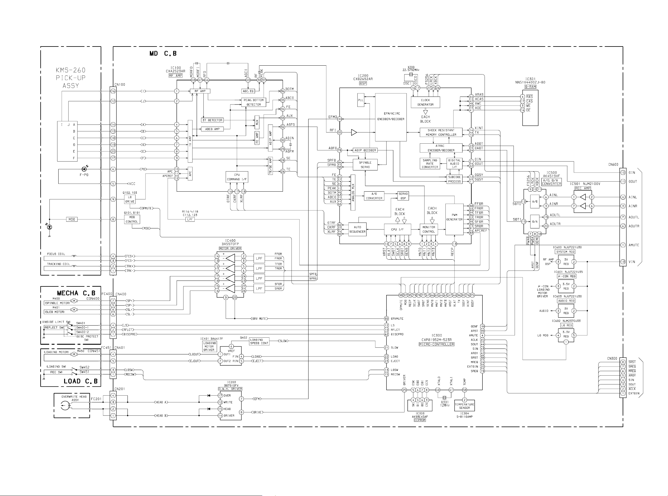
BLOCK DIAGRAM-2 (MD) .............................................................................................................. 17, 18
WIRING-1 (MAIN) ........................................................................................................................... 19, 20
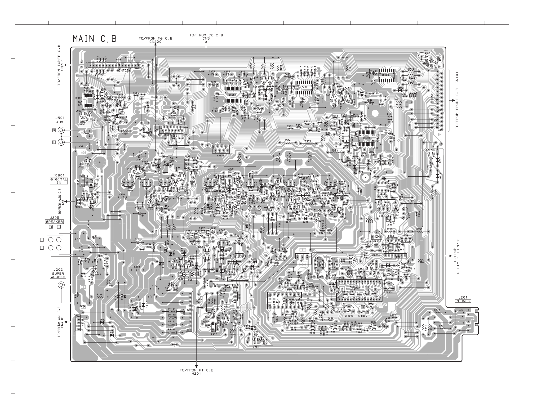
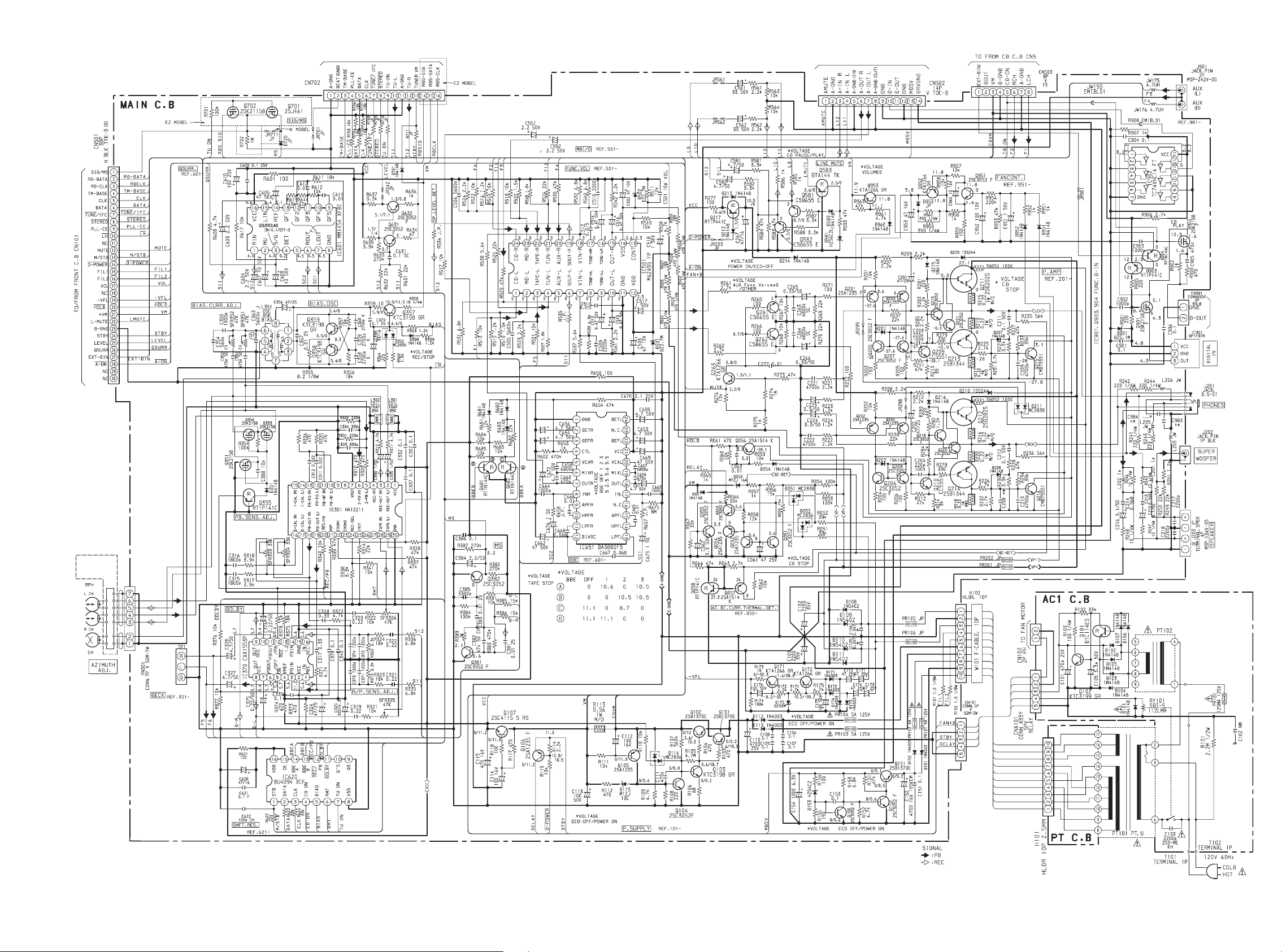
SCHEMATIC DIAGRAM-1 (MAIN).................................................................................................. 21, 22
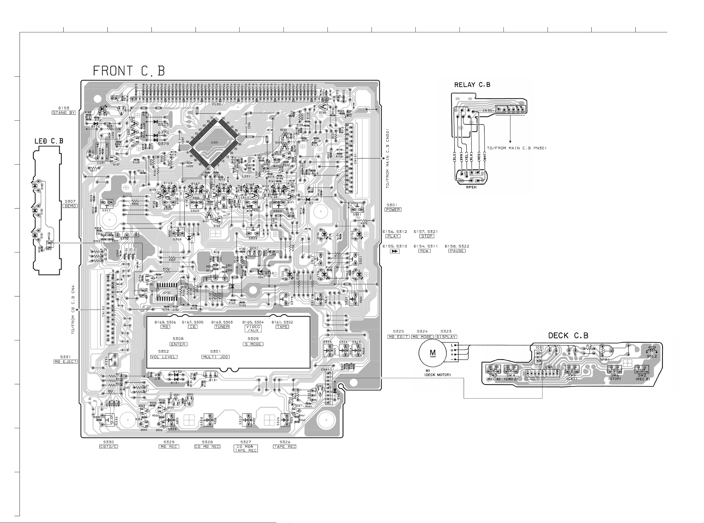
WIRING-2 (FRONT)........................................................................................................................ 23, 24
SCHEMATIC DIAGRAM-2 (FRONT) .............................................................................................. 25, 26
WIRING-3 (CD) ............................................................................................................................... 27, 28
SCHEMATIC DIAGRAM-3 (CD) ..................................................................................................... 29, 30
WIRING-4 (MD)............................................................................................................................... 31, 32
SCHEMATIC DIAGRAM-4 (MD) ..................................................................................................... 33, 34
WIRING-5 (TUNER)........................................................................................................................ 35, 36
SCHEMATIC DIAGRAM-5 (TUNER) .............................................................................................. 37, 38
WIRING-6 (AC/PT)................................................................................................................................ 39
WIRING-7 (MECHA/LOAD) .................................................................................................................. 40
FL GRID ASSIGNMENT/ANODE CONNECTION ................................................................................ 41
ELECTRICAL ADJUSTMENT/PRACTICAL SERVICE FIGURE ..................................................... 42-45
IC DESCRIPTION............................................................................................................................ 46-57
IC BLOCK DIAGRAM....................................................................................................................... 58-60
MECHANICAL EXPLODED VIEW 1/1............................................................................................ 61, 62
MECHANICAL PARTS LIST 1/1 ........................................................................................................... 63
TAPE MECHANISM PARTS LIST 1/1 .................................................................................................. 64
TAPE MECHANISM EXPLODED VIEW 1/1 ................................................................................... 65, 66
CD MECHANISM EXPLODED VIEW 1/2 ............................................................................................. 67
CD MECHANISM PARTS LIST 1/2 ...................................................................................................... 68
CD MECHANISM EXPLODED VIEW 2/2 ............................................................................................. 69
CD MECHANISM PARTS LIST 2/2 ...................................................................................................... 69
MD MECHANISM EXPLODED VIEW 1/3............................................................................................. 70
MD MECHANISM PARTS LIST 1/3...................................................................................................... 70
MD MECHANISM EXPLODED VIEW 2/3............................................................................................. 71
MD MECHANISM PARTS LIST 2/3...................................................................................................... 72
MD MECHANISM EXPLODED VIEW 3/3............................................................................................. 73
MD MECHANISM PARTS LIST 3/3...................................................................................................... 74
SPEAKER DISASSEMBLY INSTRUCTIONS....................................................................................... 75
SPEAKER PARTS LIST 1/1.................................................................................................................. 76
SPRING APPLICATION POSITION .....................................................................................................77
2
Page 3

SPECIFICATIONS
MAIN UNIT XR-MD100
FM tuner section
Tuning range 87.5 MHz to 108 MHz
Usable sensitivity (IHF) 13.2 dBf
Antenna terminals 75 ohms (unbalanced)
MW tuner section
Tuning range 531 kHz to1602 kHz (9 kHz step)
530 kHz to 1710 kHz (10 kHz
step)
Usable sensitivity 350 µV/m
Antenna Loop antenna
LW tuner section
Tuning range 144 kHz to 290 kHz
Usable sensitivity 1400 µV/m
Antenna Loop antenna
Amplifier section
Power output Rated: 25 W+25 W (6 ohms,
T.H.D. 1%,1 kHz/DIN 45500)
Reference: 30+30 W (6 ohms,
T.H.D. 10%,1 kHz/DIN 45324)
DIN MUSIC POWER
(EZ MODEL)
66.9 W+66.9 W
Inputs VIDEO/AUX: 400 mV
DIGITAL IN
sampling frequency: 48 kHz/32
kHz
Optical input level: more than
-21 dBm
Outputs SUPER WOOFER: 1.4 V
SPEAKERS: accept speakers of
6 ohms or more
PHONES (stereo minijack):
accepts headphones of 16 ohms
or more
Cassette deck section
Track format 4 tracks, 2 channels stereo
Frequency response CrO2 tape: 50 Hz–16000 Hz
Normal tape: 50 Hz–15000 Hz
Signal-to-noise ratio 60 dB (Dolby B NR ON, CrO2
tape peak level)
Recording system AC bias
Heads Deck: Recording/playback/erase
head * 1
Compact disc player section
Laser Semiconductor laser ( =780 nm)
D-A converter 1 bit dual
Signal-to-noise ratio 90 dB (1 kHz, 0 dB)
Harmonic distortion 0.05% (1 kHz,0 dB)
Wow and flutter Unmeasurable
MD recorder section
Scanning method Non-contact optical scanner
(Semiconductor laser application)
Recording system Magnetic polarity modulation
overwrite system
Rotation speed Approx.400-900 rpm (CLV)
Sampling frequency 44.1 kHz
No. of channels Stereo: 2 channels
Monaural: 1 channel
A-D, D-A converter 1-bit
Frequency 20–20000 Hz+0.2– -1.5 dB
Wow and flutter Unmeasurable
SPEAKER SYSTEM SX-M100
Cabinet type 2 way, bass reflex (magnetic
shielded type)
Speakers Woofer: 130 mm cone type
Tweeter: 60 mm cone type
Impedance 6 ohms
Output sound pressure level 87 dB/W/m
Dimensions (W * H * D) 175 * 275 * 227 mm
Weight 3.0 kg
General
Power requirements 230 V AC, 50 Hz
Power consumption 80 W
Standby power consumption 1.4 W (power-economizing mode
set to ON)
Dimensions (W * H * D) 175 * 275 * 333 mm
Weight 6.0 kg
Design and specifications are subject to change without
•
notice.
Dolby noise reduction manufactured under license from
•
Dolby Laboratories Licensing Corporation.
“DOLBY” and the double-D symbol
of Dolby Laboratories Licensing Corporation.
The word “BBE” and the “BBE symbol” are trademarks
•
of BBE Sound,Inc.
Under license from BBE Sound,Inc.
are trademarks
ACCESSORIES/PACKAGE LIST
REF. NO PART NO. KANRI DESCRIPTION
NO.
1 87-A90-118-010 ANT,WIRE FM (Z)
2 87-A90-030-010 ANT,LOOP AM-NC C
3 8Z-CL4-906-010 IB,EZ(9L)S<EZ>
3 8Z-CL4-905-010 IB,K(E)S<K>
4 8Z-CK4-952-010 RC UNIT,RC-ZAT04
3
Page 4
PROTECTION OF EYES FROM LASER BEAM DURING SERVICING
This set employs laser. Therefore, be sure to follow carefully the
instructions below when servicing.
WARNING!
WHEN SERVICING, DO NOT APPROACH THE LASER EXIT
WITH THE EYE TOO CLOSELY. IN CASE IT IS NECESSARY TO
CONFIRM LASER BEAM EMISSION. BE SURE TO OBSERVE
FROM A DISTANCE OF MORE THAN 30cm FROM THE
SURFACE OF THE OBJECTIVE LENS ON THE OPTICAL
PICK-UP BLOCK.
Caution: Invisible laser radiation when
open and interlocks defeated avoid exposure to beam.
Advarsel:Usynling laserståling ved åbning,
når sikkerhedsafbrydere er ude af funktion.
Undgå udsættelse for stråling.
VAROITUS!
Laiteen Käyttäminen muulla kuin tässä käyttöohjeessa mainitulla tavalla saattaa altistaa käyt-täjän turvallisuusluokan 1 ylittävälle näkymättömälle lasersäteilylle.
VARNING!
Om apparaten används på annat sätt än vad som specificeras i
denna bruksanvising, kan användaren utsättas för osynling
laserstrålning, som överskrider gränsen för laserklass 1.
CAUTION
Use of controls or adjustments or performance of procedures
other than those specified herein may result in hazardous
radiation exposure.
ATTENTION
L'utilisation de commandes, réglages ou procédures autres que
ceux spécifiés peut entraîner une dangereuse exposition aux
radiations.
ADVARSEL!
Usynlig laserståling ved åbning, når sikkerhedsafbrydereer ude
af funktion. Undgå udsættelse for stråling.
This Compact Disc player is classified as a CLASS 1 LASER
product.
The CLASS 1 LASER PRODUCT label is located on the rear
exterior.
CLASS 1
KLASSE 1
LUOKAN 1
KLASS 1
LASER PRODUCT
LASER PRODUKT
LASER LAITE
LASER APPARAT
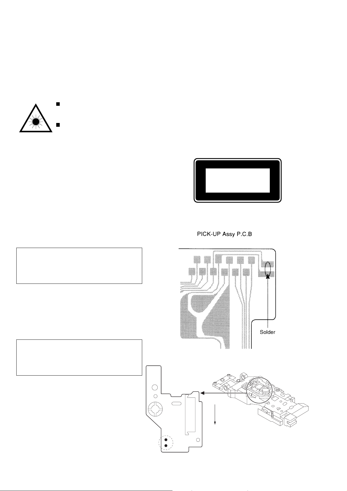
Precaution to replace Optical block
(KSS-213F)
Body or clothes electrostatic potential could ruin
laser diode in the optical block. Be sure ground
body and workbench, and use care the clothes
do not touch the diode.
1) After the connection, remove solder shown in
the right figure.
Precaution to replace Optical block
(KMS-260A)
Body or clothes electrostatic potential could ruin
laser diode in the optical block. Be sure ground
body and workbench, and use care the clothes
do not touch the diode.
1) After the connection, remove solder
shown in the right figure.
1 VEE
¡ TRK –
4
Page 5
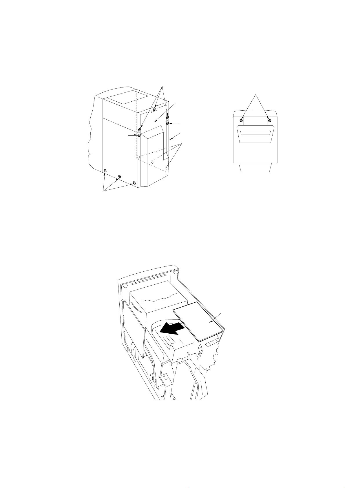
DISASSEMBLY INSTRUCTIONS
Disassembly Procedure
1. Open the cabinet
1) Remove the screws (1BVT2+3-10*1, 2UTT2+3-6*3 w/o SLOT B), and remove the PANEL SIDE L.
2) Remove the screws (3BVT2+3-10*1, 4UTT2+3-6*3 w/o SLOT B), and remove the PANEL SIDE R.
3) Remove the screw (5BVT2+3-10*3) from the rear side, open the deck lid, remove the screw (6BVT2+3-16*2), and remove
the TOP PANEL.
5
6
REAR PANEL
3
1
PANEL
SIDE L
2
4) Remove the screw (BVT2+3-10*11) from the rear side, and remove the REAR PANEL.
PANEL SIDE R
4
2. Removing the deck mechanism.
1) Remove the TUNER C.B in the direction of the arrow.
TOP PANEL
TUNER C.B
5
Page 6
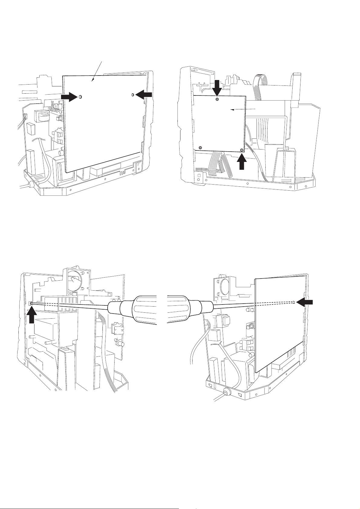
2) Remove the screw (7BVT2+3-10*2) on the top of the MAIN C.B, and remove the screw (8BVT2+3-10*3) from the CD C.B.
MAIN C.B
8
7
3) Remove the CD C.B, remove the screw (9UTT2+3-6*1), insert a screwdriver tip through the clearance between the parts and
the chassis, and remove the screw (0UTT2+3-6*1).
7
CD C.B
8
9
AC
C.B
4) Remove the cord, and remove the deck mechanism together with the chassis.
0
MAIN C.B
6
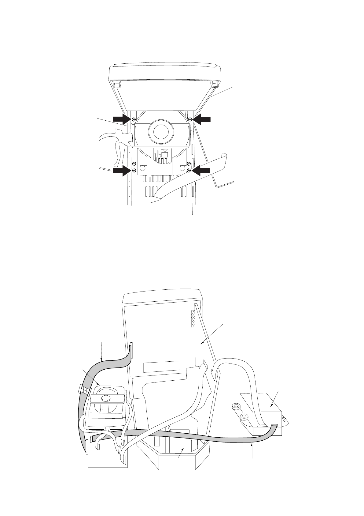
Page 7
3. Removing the MD mechanism.
1) Remove the screw (!BVTT+4-6*4) securing the transformer, and move the transformer to the rear.
2) Remove the screw (@BVT2+3-10*1) that fixes the heat side to the holder, and remove the MAIN C.B.
!
@
3) Remove the screw (#BVT2+3-10*4), and remove the MD mechanism together with the chassis.
#
#
AC
C.B
MD chassis
MD chassis
MD mechanism
# #
MD chassis
Upper side
7
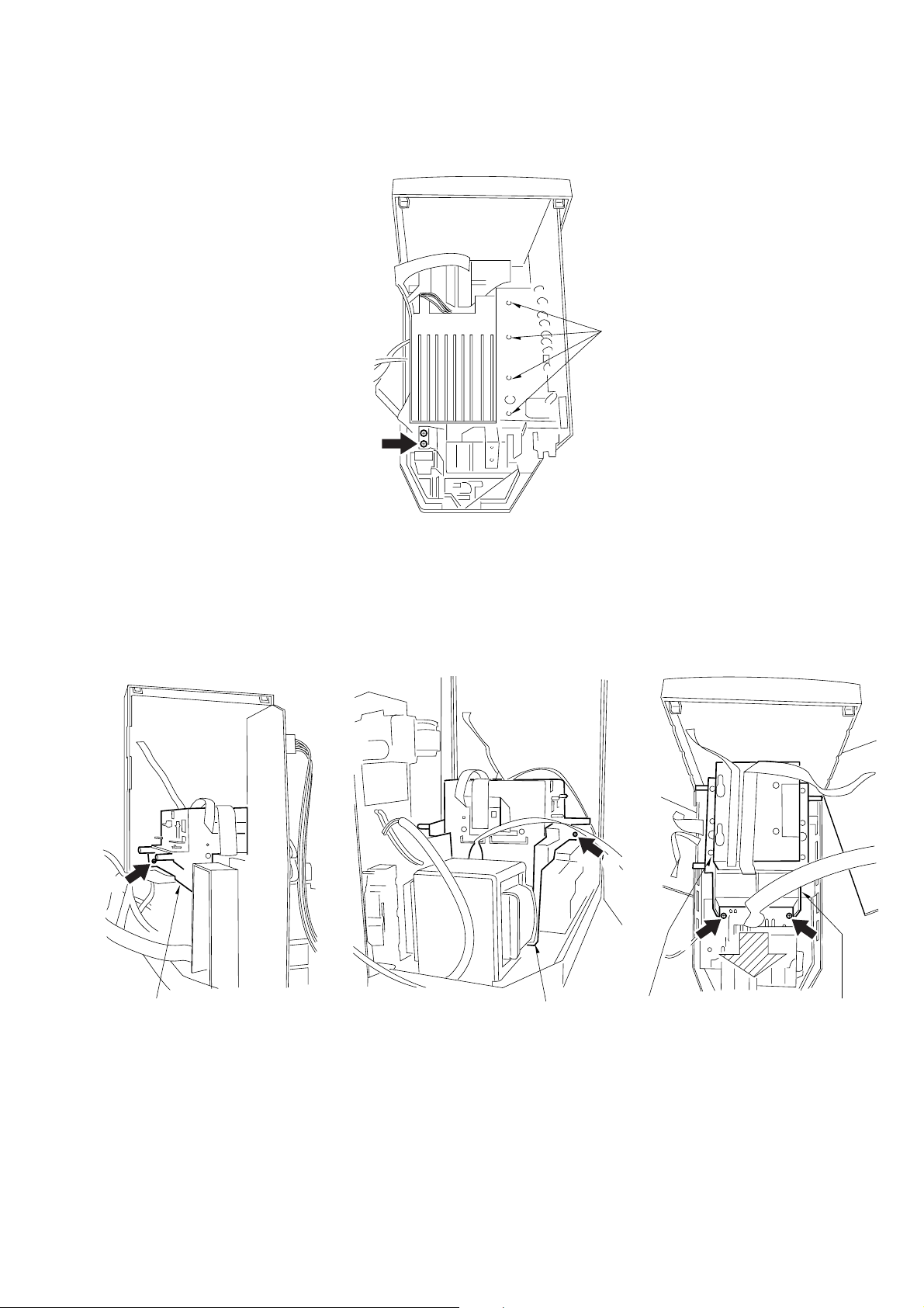
Page 8
4. Removing the CD mechanism.
1) Remove the screw ($BVT2+3-6*4), open the tray, remove the CD panel, and remove the CD mechanism.
$
$
Upper side
SERVICE JIG AND TOOLS
After opening the board, use the following jig and tools as shown in the figure.
JIG. EX TENSION (TANAKA) ...................SV-J00-019-010
FFC, 8P-1.0 ...................................................SV-J00-043-010
$
$
Extension FFC
(JIG, EXTENSION (TANAKA))
CD mechanism
Component side of CD C.B
FRONT C.B
Heat sink
Transformer
Rear side of the unit
MAIN C.B
MD mechanism
Extension FFC (FFC, 8P-1.0)
8
Page 9

ELECTRICAL MAIN PARTS LIST
REF. NO PART NO. KANRI DESCRIPTION
NO.
IC
87-A20-446-010 C-IC,LA9241ML
87-A20-459-010 C-IC,LC78622ED
87-A20-445-010 IC,BA5936
87-070-289-040 IC,BU 2092F
8Z-CL4-620-010 IC,LC87F65C8A
87-A20-914-010 IC,SPS-442-1-F
87-A20-455-010 IC,HA12211
87-A20-355-010 IC,CXA1553P
87-A21-111-040 C-IC,M62495FP
87-A21-103-040 C-IC,MM1454XFBE
87-017-915-080 IC,BU4094BCF
87-A21-022-040 C-IC,BA3880FS
87-A20-870-010 IC,GP1F37R
87-A21-175-040 C-IC,TC74VHC14FT
87-070-127-110 IC,LC72131 D
87-A20-913-010 IC,LA1837NL
87-A20-440-040 C-IC,BU1920FS
87-A20-707-010 C-IC,CXA2523AR
87-A20-708-010 C-IC,CXD2652AR
87-A20-709-040 C-IC,BD7910FV
87-ZG9-607-010 C-IC,CXP81952M-523R
87-ZG9-606-040 C-IC,MN41V4400SJ-08
87-A20-755-080 C-IC,AK93C45AF
87-A20-710-040 C-IC,S-8110AMP
87-A20-711-040 C-IC,BA5970FP
87-A20-712-040 C-IC,BA6417F
87-A21-110-040 C-IC,AK4519VF
87-017-853-040 IC,NJM2100V
87-A20-797-040 C-IC,NJU7221U30
87-A20-798-040 C-IC,NJU7221U35
87-A20-714-040 C-IC,NJM2370U33
TRANSISTOR
87-026-463-080 TR,2SA933S (0.3W)
87-026-239-080 TR,DTC114TK (0.2W)
87-A30-076-080 C-TR,2SC3052F
87-A30-075-080 C-TR,2SA1235F
87-A30-268-040 C-TR,2SA1514K(S)
87-A30-074-080 C-TR,RT1P 141C
89-113-187-880 TRNSISTOR,2SA1318 (0.5W)
87-A30-047-080 TR,CSD655E
89-213-702-010 TR,2SB1370 (1.8W)
87-026-245-080 TR,DTC114ES
87-A30-198-080 TR,KTC3199GR
87-026-610-080 TR,KTC3198GR
87-A30-196-080 TR,2SC4115SRS
87-A30-072-080 C-TR,RT1P 144C
87-A30-073-080 C-TR,RT1N 141C
87-A30-087-080 C-FET,2SK2158
87-026-609-080 TR,KTA1266GR
87-A30-190-080 TR,CC5551
87-A30-215-010 TR,2SD2025
87-A30-214-010 TR,2SB1344
87-A30-106-070 C-TR,CMBT5551
87-A30-105-080 C-TR,RT1P 441C
87-A30-159-080 C-TR,KTA1298Y
87-A30-084-080 TR,CSB1058B
89-327-143-080 TR,2SC2714 (0.1W)
87-026-297-080 TR,DTA144TK
87-A30-071-080 C-TR,RT1N 144C
87-A30-234-080 TR,CSC4115BC
87-A30-072-080 C-TR,RT1P 144
89-327-143-080 TR,2SC2714 (0.1W)
87-A30-076-080 C-TR,2SC3052F<K>
87-A30-074-080 C-TR,RT1P 141C
87-A30-086-070 C-TR,CSD1306E
89-505-434-540 C-FET,2SK543(4/5)
REF. NO PART NO. KANRI DESCRIPTION
NO.
87-026-423-080 C-TR RN2305
89-115-884-080 CHIP -TRANSISTER 2SA1588Y
89-341-164-080 CHIP-TRANSISTOR,2SC4116 Y
87-026-412-080 C-TR RN1305
DIODE
87-A40-291-080 DIODE,1N4148 (CPT)
87-A40-270-080 C-DIODE,MC2838
87-A40-269-080 C-DIODE,MC2836
87-A40-004-080 ZENER,MTZJ16A
87-070-178-090 DIODE,1N5402-BD54
87-070-274-080 DIODE,1N4003 SEM
87-A40-345-080 ZENER,MTZJ10C
87-017-083-080 ZENER,HZS4C2
87-A40-312-080 ZENER,DZ33M
87-A40-488-080 DIODE,1SS244
87-A40-509-080 ZENER,MTZJ6.8C
87-A40-293-080 ZENER,DZ2.7M
87-001-731-080 ZENER,HZS6C2L
87-A40-299-080 ZENER,DZ5.1M
87-017-149-080 ZENER,HZS6A2L
87-020-465-080 DIODE,1SS133 (110MA)
87-A40-270-080 C-DIODE,MC2838
87-001-166-080 DIODE,1SS301
87-A40-412-040 C-DIODE,SB05-05CP
MAIN C.B
C61 87-010-260-080 CAP, ELECT 47-25V
C62 87-010-403-080 CAP, ELECT 3.3-50V
C63 87-010-197-080 CAP, CHIP 0.01 DM
C102 87-016-051-090 CAP,E 2200-35 SMG
C103 87-A10-479-080 CAP,CER 2200P-250 M E KH
C106 87-010-196-080 CHIP CAPACITOR,0.1-25
C107 87-010-196-080 CHIP CAPACITOR,0.1-25
C108 87-010-196-080 CHIP CAPACITOR,0.1-25
C109 87-010-196-080 CHIP CAPACITOR,0.1-25
C110 87-010-928-090 CAP,E 4700-25 SMG
C111 87-012-140-080 CAP 470P
C112 87-010-112-080 CAP, ELECT 100-16V
C113 87-010-247-080 CAP, ELECT 100-50V
C114 87-010-112-080 CAP, ELECT 100-16V
C115 87-010-235-080 CAP,E 470-16 SME
C151 87-010-196-080 CHIP CAPACITOR,0.1-25
C152 87-A11-233-090 CAP,E 4700-16 105 KMG
C153 87-010-196-080 CHIP CAPACITOR,0.1-25
C154 87-A10-105-080 CAP,E 1000-6.3 REA
C171 87-010-260-080 CAP, ELECT 47-25V
C172 87-010-260-080 CAP, ELECT 47-25V
C173 87-010-260-080 CAP, ELECT 47-25V
C174 87-010-260-080 CAP, ELECT 47-25V
C175 87-010-247-080 CAP, ELECT 100-50V
C176 87-010-247-080 CAP, ELECT 100-50V
C201 87-010-260-080 CAP, ELECT 47-25V
C202 87-010-260-080 CAP, ELECT 47-25V
C203 87-A10-946-080 C-CAP,S 220P-100 J CH
C204 87-A10-946-080 C-CAP,S 220P-100 J CH
C209 87-010-186-080 CAP,CHIP 4700P
C210 87-010-186-080 CAP,CHIP 4700P
C211 87-012-368-080 C-CAP,S 0.1-50 F
C212 87-012-368-080 C-CAP,S 0.1-50 F
C213 87-010-195-080 C-CAP,S 0.068-25 F
C214 87-015-837-080 C-CAP,0.068 F
C215 87-010-544-080 CAP, ELECT 0.1-50V
C216 87-010-544-080 CAP, ELECT 0.1-50V
C217 87-010-182-080 C-CAP,S 2200P-50 B
C218 87-010-182-080 C-CAP,S 2200P-50 B
C221 87-010-186-080 CAP,CHIP 4700P
C222 87-010-186-080 CAP,CHIP 4700P
9
Page 10

REF. NO PART NO. KANRI DESCRIPTION
C223 87-010-403-080 CAP, ELECT 3.3-50V
C224 87-010-403-080 CAP, ELECT 3.3-50V
C265 87-010-546-080 CAP, ELECT 0.33-50V
C266 87-010-546-080 CAP, ELECT 0.33-50V
C267 87-010-380-080 CAP, ELECT 47-16V
C267 87-010-380-080 CAP, ELECT 47-16V
C277 87-010-197-080 CAP, CHIP 0.01 DM
C303 87-012-157-080 C-CAP,S 330P-50 CH
C304 87-012-157-080 C-CAP,S 330P-50 CH
C307 87-010-196-080 CHIP CAPACITOR,0.1-25
C311 87-010-198-080 CAP, CHIP 0.022
C312 87-010-198-080 CAP, CHIP 0.022
C315 87-010-181-080 CAP,CHIP S 1800P
C316 87-010-181-080 CAP,CHIP S 1800P
C317 87-012-142-080 CAP, S 0.33-16
C318 87-012-142-080 CAP, S 0.33-16
C319 87-012-141-080 CHIP-CAPACITOR,0.22-16F
C320 87-012-141-080 CHIP-CAPACITOR,0.22-16F
C321 87-012-141-080 CHIP-CAPACITOR,0.22-16F
C322 87-012-141-080 CHIP-CAPACITOR,0.22-16F
C324 87-010-260-080 CAP, ELECT 47-25V
C325 87-010-370-080 CAP,E 330-6.3 SME
C327 87-010-404-080 CAP, ELECT 4.7-50V
C328 87-010-404-080 CAP, ELECT 4.7-50V
C332 87-010-196-080 CHIP CAPACITOR,0.1-25
C335 87-010-401-080 CAP, ELECT 1-50V
C336 87-010-401-080 CAP, ELECT 1-50V
C337 87-010-196-080 CHIP CAPACITOR,0.1-25
C339 87-010-196-080 CHIP CAPACITOR,0.1-25
C340 87-010-196-080 CHIP CAPACITOR,0.1-25
C351 87-012-140-080 CAP 470P
C352 87-012-140-080 CAP 470P
C354 87-010-175-080 CAP 560P
C355 87-010-178-080 CHIP CAP 1000P
C356 87-010-260-080 CAP, ELECT 47-25V
C357 87-010-197-080 CAP, CHIP 0.01 DM
C358 87-010-183-080 C-CAP,S 2700P-50 B
C359 87-010-183-080 C-CAP,S 2700P-50 B
C360 87-010-183-080 C-CAP,S 2700P-50 B
C370 87-010-196-080 CHIP CAPACITOR,0.1-25
C371 87-010-179-080 CAP,CHIP S B1200P
C372 87-010-179-080 CAP,CHIP S B1200P
C373 87-010-179-080 CAP,CHIP S B1200P
C374 87-010-179-080 CAP,CHIP S B1200P
C375 87-010-545-080 CAP, ELECT 0.22-50V
C376 87-010-545-080 CAP, ELECT 0.22-50V
C378 87-018-209-080 CAP, CER 0.1-50V
C381 87-010-197-080 CAP, CHIP 0.01 DM
C382 87-010-318-080 C-CAP,S 47P-50 CH
C383 87-010-197-080 CAP, CHIP 0.01 DM
C384 87-010-402-080 CAP, ELECT 2.2-50V
C385 87-010-184-080 CHIP CAPACITOR 3300P(K)
C386 87-010-196-080 CHIP CAPACITOR,0.1-25
C388 87-010-154-080 CAP CHIP 10P
C399 87-010-265-080 CAP, ELECT 33-16V
C501 87-010-154-080 CAP CHIP 10P
C502 87-010-374-080 CAP, ELECT 47-10V
C503 87-010-374-080 CAP, ELECT 47-10V
C505 87-010-187-080 CAP CHIP S5600P
C506 87-010-187-080 CAP CHIP S5600P
C509 87-010-182-080 C-CAP,S 2200P-50 B
C510 87-010-182-080 C-CAP,S 2200P-50 B
C511 87-010-213-080 C-CAP,S 0.015-50 B
C512 87-010-213-080 C-CAP,S 0.015-50 B
C513 87-010-400-080 CAP, ELECT 0.47-50V
C514 87-010-400-080 CAP, ELECT 0.47-50V
C515 87-010-400-080 CAP, ELECT 0.47-50V
C516 87-010-400-080 CAP, ELECT 0.47-50V
C517 87-010-401-080 CAP, ELECT 1-50V
C518 87-010-401-080 CAP, ELECT 1-50V
C551 87-010-402-080 CAP, ELECT 2.2-50V
C552 87-010-402-080 CAP, ELECT 2.2-50V
C561 87-010-407-080 CAP, ELECT 33-50V
C562 87-010-407-080 CAP, ELECT 33-50V
C581 87-010-404-080 CAP, ELECT 4.7-50V
NO.
REF. NO PART NO. KANRI DESCRIPTION
C582 87-010-404-080 CAP, ELECT 4.7-50V
C603 87-010-402-080 CAP, ELECT 2.2-50V
C604 87-010-402-080 CAP, ELECT 2.2-50V
C605 87-010-408-080 CAP, ELECT 47-50V
C607 87-010-405-080 CAP, ELECT 10-50V
C608 87-010-405-080 CAP, ELECT 10-50V
C609 87-010-196-080 CHIP CAPACITOR,0.1-25
C610 87-010-384-080 CAP, ELECT 100-25V
C611 87-010-197-080 CAP, CHIP 0.01 DM
C612 87-010-197-080 CAP, CHIP 0.01 DM
C620 87-010-380-080 CAP, ELECT 47-16V
C621 87-010-196-080 CHIP CAPACITOR,0.1-25
C622 87-010-322-080 C-CAP,S 100P-50 CH
C631 87-010-400-080 CAP, ELECT 0.47-50V
C653 87-010-404-080 CAP, ELECT 4.7-50V
C654 87-010-404-080 CAP, ELECT 4.7-50V
C655 87-010-404-080 CAP, ELECT 4.7-50V
C656 87-010-404-080 CAP, ELECT 4.7-50V
C657 87-010-188-080 CAP,CHIP 6800P
C658 87-010-188-080 CAP,CHIP 6800P
C659 87-012-140-080 CAP 470P
C660 87-012-140-080 CAP 470P
C662 87-010-408-080 CAP, ELECT 47-50V
C663 87-010-178-080 CHIP CAP 1000P
C664 87-010-178-080 CHIP CAP 1000P
C665 87-010-197-080 CAP, CHIP 0.01 DM
C666 87-010-197-080 CAP, CHIP 0.01 DM
C667 87-010-195-080 C-CAP,S 0.068-25 F
C668 87-010-195-080 C-CAP,S 0.068-25 F
C669 87-010-408-080 CAP, ELECT 47-50V
C670 87-010-196-080 CHIP CAPACITOR,0.1-25
C671 87-010-404-080 CAP, ELECT 4.7-50V
C672 87-010-404-080 CAP, ELECT 4.7-50V
C675 87-010-401-080 CAP, ELECT 1-50V
C676 87-010-401-080 CAP, ELECT 1-50V
C901 87-010-196-080 CHIP CAPACITOR,0.1-25
C902 87-010-178-080 CHIP CAP 1000P
C903 87-010-178-080 CHIP CAP 1000P
C904 87-010-196-080 CHIP CAPACITOR,0.1-25
C905 87-012-140-080 CAP 470P
C906 87-010-196-080 CHIP CAPACITOR,0.1-25
C951 87-010-401-080 CAP, ELECT 1-50V
C952 87-010-263-080 CAP, ELECT 100-10V
C953 87-010-380-080 CAP, ELECT 47-16V
C960 87-010-405-080 CAP, ELECT 10-50V
CN101 87-A60-111-010 CONN,5P V S2M 5W
CN501 87-099-719-010 CONN,30P TYK-B(X)
CN502 87-A60-423-010 CONN,14P V TOC-B
CN503 87-A60-133-010 CONN,8P V FE
CN702 87-A60-189-010 CONN,16P V TUC-P16P-B1
CN901 8Z-CL4-656-010 CONN ASSY,2P V DTL SHLD
J201 87-A60-420-010 JACK,3.5 ST (MSC)
J202 87-099-801-010 JACK,PIN 1P BLK
J203 87-A60-659-010 TERMINAL,SPKR 4P HSP-134V-05Z
L201 87-003-383-010 COIL,1UH-S
L202 87-003-383-010 COIL,1UH-S
L301 87-A50-049-010 COIL,TRAP 85K(COI)
L302 87-A50-049-010 COIL,TRAP 85K(COI)
L351 87-007-342-010 COIL,OSC 85K BIAS
PN301 87-A60-112-010 CONN,7P V S2M-7W
!
PR103 87-026-681-080 PROTECTOR,5A 60V 491
!
PR104 87-026-681-080 PROTECTOR,5A 60V 491
!
PR151 87-A90-094-080 PROTECTOR,4A 491SERIES 60V
!
PR152 87-A90-094-080 PROTECTOR,4A 491SERIES 60V
R215 87-A00-258-080 RES,M/F 0.22-1W J
R216 87-A00-258-080 RES,M/F 0.22-1W J
R217 87-A00-258-080 RES,M/F 0.22-1W J
R218 87-A00-258-080 RES,M/F 0.22-1W J
R219 87-A00-258-080 RES,M/F 0.22-1W J
R220 87-A00-258-080 RES,M/F 0.22-1W J
R908 87-008-372-080 FILTER, EMI BL OIRNI
SFR303 87-A90-557-080 SFR,33K H HOKU
SFR304 87-A90-557-080 SFR,33K H HOKU
SFR305 87-024-436-080 SFR,47K RH063EC
SFR306 87-024-436-080 SFR,47K RH063EC
NO.
10
Page 11

REF. NO PART NO. KANRI DESCRIPTION
NO.
SFR351 87-024-436-080 SFR,47K RH063EC
SFR352 87-024-436-080 SFR,47K RH063EC
TH51 87-A91-042-080 C-THMS,100K 55001
TH52 87-A91-042-080 C-THMS,100K 55001
W101 8Z-CL4-658-010 F-CABLE,10P 2.5 300MM
CD C.B
C1 87-010-403-080 CAP, ELECT 3.3-50V
C2 87-010-197-080 CAP, CHIP 0.01 DM
C3 87-010-263-080 CAP, ELECT 100-10V
C4 87-010-248-080 CAP, ELECT 220-10V
C5 87-010-197-080 CAP, CHIP 0.01 DM
C6 87-010-374-080 CAP, ELECT 47-10V
C7 87-012-349-080 C-CAP,S 1000P-50 CH
C8 87-010-198-080 CAP, CHIP 0.022
C9 87-010-248-080 CAP, ELECT 220-10V
C10 87-010-263-080 CAP, ELECT 100-10V
C12 87-010-401-080 CAP, ELECT 1-50V
C13 87-010-193-080 CHIP CAPACITOR,0.033
C14 87-010-405-080 CAP, ELECT 10-50V
C17 87-012-157-080 C-CAP,S 330P-50 CH
C18 87-010-213-080 C-CAP,S 0.015-50 B
C20 87-010-193-080 CHIP CAPACITOR,0.033
C22 87-010-183-080 C-CAP,S 2700P-50 B
C23 87-010-956-080 CHIP-CAP,S 0.068-25B
C25 87-010-994-080 C-CAP,S 680P-50 CH
C29 87-010-186-080 CAP,CHIP 4700P
C30 87-012-156-080 C-CAP,S 220P-50 CH
C31 87-010-400-080 CAP, ELECT 0.47-50V
C32 87-010-374-080 CAP, ELECT 47-10V
C33 87-010-401-080 CAP, ELECT 1-50V
C34 87-010-184-080 CHIP CAPACITOR 3300P(K)
C35 87-010-197-080 CAP, CHIP 0.01 DM
C36 87-010-374-080 CAP, ELECT 47-10V
C37 87-010-404-080 CAP, ELECT 4.7-50V
C38 87-010-196-080 CHIP CAPACITOR,0.1-25
C40 87-010-145-080 C-CAP,S 1P-50 CH
C42 87-010-312-080 C-CAP,S 15P-50 CH
C45 87-010-196-080 CHIP CAPACITOR,0.1-25
C46 87-010-196-080 CHIP CAPACITOR,0.1-25
C47 87-010-196-080 CHIP CAPACITOR,0.1-25
C48 87-010-315-080 C-CAP,S 27P-50 CH
C50 87-012-140-080 CAP 470P
C51 87-012-156-080 C-CAP,S 220P-50 CH
C52 87-012-140-080 CAP 470P
C53 87-010-322-080 C-CAP,S 100P-50 CH
C54 87-012-153-080 C-CAP,S 120P-50 CH
C55 87-010-263-080 CAP, ELECT 100-10V
C57 87-010-316-080 C-CAP,S 33P-50 CH
C58 87-010-316-080 C-CAP,S 33P-50 CH
C59 87-010-263-080 CAP, ELECT 100-10V
C60 87-010-196-080 CHIP CAPACITOR,0.1-25
C61 87-010-196-080 CHIP CAPACITOR,0.1-25
C62 87-A10-373-080 CAP,E 220-6.3 M SSL
C65 87-010-404-080 CAP, ELECT 4.7-50V
C66 87-010-196-080 CHIP CAPACITOR,0.1-25
C67 87-010-263-080 CAP, ELECT 100-10V
C69 87-012-154-080 C-CAP,S 150P-50 CH
C75 87-010-197-080 CAP, CHIP 0.01 DM
C76 87-A10-102-080 CAP,E 1000-10 REA
C77 87-010-197-080 CAP, CHIP 0.01 DM
C78 87-010-221-080 CAP, ELECT 470-10V
C79 87-010-263-080 CAP, ELECT 100-10V
C80 87-010-197-080 CAP, CHIP 0.01 DM
C81 87-010-405-080 CAP, ELECT 10-50V
C82 87-010-405-080 CAP, ELECT 10-50V
C83 87-010-181-080 CAP,CHIP S 1800P
C84 87-010-181-080 CAP,CHIP S 1800P
C90 87-010-196-080 CHIP CAPACITOR,0.1-25
C91 87-010-408-080 CAP, ELECT 47-50V
C92 87-010-382-080 CAP, ELECT 22-25V
C93 87-010-197-080 CAP, CHIP 0.01 DM
C94 87-010-197-080 CAP, CHIP 0.01 DM
C95 87-010-197-080 CAP, CHIP 0.01 DM
REF. NO PART NO. KANRI DESCRIPTION
NO.
C101 87-010-322-080 C-CAP,S 100P-50 CH
C102 87-010-322-080 C-CAP,S 100P-50 CH
C103 87-010-322-080 C-CAP,S 100P-50 CH
C104 87-010-322-080 C-CAP,S 100P-50 CH
C105 87-010-322-080 C-CAP,S 100P-50 CH
C110 87-010-196-080 CHIP CAPACITOR,0.1-25
CN1 87-A60-424-010 CONN,16P V TOC-B
CN2 87-A60-131-010 CONN,6P V FE
CN3 87-A60-130-010 CONN,5P V FE
CN4 87-099-719-010 CONN,30P TYK-B(X)
CN5 87-A60-133-010 CONN,8P V FE
CN6 87-A60-422-010 CONN,8P V TOC-B
CNA1 87-A60-109-010 CONN,2P V S2M-2W
L1 87-003-102-080 COIL, 10UH
L4 87-003-152-080 COIL, 100UH
L5 87-003-152-080 COIL, 100UH
SFR130 87-024-437-080 SFR100K,RH063EC
X1 87-A70-046-010 VIB,XTAL 16.934MHZ
FRONT C.B
C131 87-010-402-040 CAP,E 2.2-50 SME
C132 87-010-400-040 CAP,E 0.47-50
C151 87-010-196-080 CHIP CAPACITOR,0.1-25
C152 87-010-322-080 C-CAP,S 100P-50 CH
C201 87-012-145-080 CAP, CHIP S 270P CH
C203 87-018-149-080 CAP,TC-U 15P-50 CH
C204 87-015-785-080 CHIP CAPACITOR, 0.1FZ-25Z
C205 87-010-196-080 CHIP CAPACITOR,0.1-25
C206 87-018-209-080 CAP, CER 0.1-50V
C207 87-018-209-080 CAP, CER 0.1-50V
C231 87-010-405-040 CAP,E 10-50
C232 87-010-178-080 CHIP CAP 1000P
C241 87-010-400-040 CAP,E 0.47-50
C242 87-A10-189-040 CAP,E 220-10
C243 87-010-196-080 CHIP CAPACITOR,0.1-25
C245 87-010-378-040 CAP,E 10-16
C246 87-010-196-080 CHIP CAPACITOR,0.1-25
C247 87-010-194-080 CAP, CHIP 0.047
C249 87-018-208-080 CAP 0.047-50F
C250 87-010-198-080 CAP, CHIP 0.022
C251 87-010-263-040 CAP,E 100-10
C351 87-010-197-080 CAP, CHIP 0.01 DM
C352 87-010-197-080 CAP, CHIP 0.01 DM
C353 87-010-197-080 CAP, CHIP 0.01 DM
C354 87-010-197-080 CAP, CHIP 0.01 DM
C371 87-010-421-040 CAP,E 4.7-50 5L
C372 87-010-421-040 CAP,E 4.7-50 5L
C373 87-010-408-040 CAP,E 47-50 SME
C501 87-010-196-080 CHIP CAPACITOR,0.1-25
CN101 87-099-720-010 CONN,30P TYK-B(P)
CN102 87-099-720-010 CONN,30P TYK-B(P)
CNA401 88-802-092-420 CONN ASSY,9P
D153 87-A40-568-010 LED,L-13HD RED
D154 87-001-161-080 LED SEL2410E
D155 87-001-161-080 LED SEL2410E
D156 87-001-161-080 LED SEL2410E
D157 87-001-161-080 LED SEL2410E
D158 87-001-161-080 LED SEL2410E
D161 87-A40-276-080 LED,SML1816W UMB/GRN
D163 87-A40-276-080 LED,SML1816W UMB/GRN
D165 87-A40-276-080 LED,SML1816W UMB/GRN
D167 87-A40-276-080 LED,SML1816W UMB/GRN
D169 87-A40-276-080 LED,SML1816W UMB/GRN
FL301 8Z-CL4-621-010 FL,13-ST-36GNK
L201 87-A50-052-010 COIL,CLOCK 5.76MHZ T1
S301 87-A90-696-080 SW,TACT TS2103-03-430
S302 87-A90-696-080 SW,TACT TS2103-03-430
S303 87-A90-696-080 SW,TACT TS2103-03-430
S304 87-A90-696-080 SW,TACT TS2103-03-430
S305 87-A90-696-080 SW,TACT TS2103-03-430
S306 87-A90-696-080 SW,TACT TS2103-03-430
S307 87-A90-696-080 SW,TACT TS2103-03-430
S308 87-A90-696-080 SW,TACT TS2103-03-430
S309 87-A90-696-080 SW,TACT TS2103-03-430
11
Page 12

REF. NO PART NO. KANRI DESCRIPTION
NO.
S310 87-A90-696-080 SW,TACT TS2103-03-430
S311 87-A90-696-080 SW,TACT TS2103-03-430
S312 87-A90-696-080 SW,TACT TS2103-03-430
S321 87-A90-696-080 SW,TACT TS2103-03-430
S322 87-A90-696-080 SW,TACT TS2103-03-430
S323 87-A90-696-080 SW,TACT TS2103-03-430
S324 87-A90-696-080 SW,TACT TS2103-03-430
S325 87-A90-696-080 SW,TACT TS2103-03-430
S326 87-A90-696-080 SW,TACT TS2103-03-430
S327 87-A90-696-080 SW,TACT TS2103-03-430
S328 87-A90-696-080 SW,TACT TS2103-03-430
S329 87-A90-696-080 SW,TACT TS2103-03-430
S330 87-A90-696-080 SW,TACT TS2103-03-430
S331 87-A90-696-080 SW,TACT TS2103-03-430
S351 87-A90-085-010 SW,RTRY EC16B 24204
S352 87-A90-535-010 SW,RTRY EC16B24304
LED C.B
D181 87-001-161-080 LED SEL2410E
D182 87-002-738-080 LED,SEL2210R TP6
D183 87-001-161-080 LED SEL2410E
TUNER C.B
C701 87-010-381-080 CAP, ELECT 330-16V
C702 87-010-404-080 CAP, ELECT 4.7-50V
C703 87-012-286-080 CAP, U 0.01-25
C704 87-012-286-080 CAP, U 0.01-25
C709 87-012-195-080 C-CAP,U 100P-50CH
C711 87-010-260-080 CAP, ELECT 47-25V
C712 87-010-831-080 C-CAP,U,0.1-16F
C713 87-012-286-080 CAP, U 0.01-25
C714 87-012-286-080 CAP, U 0.01-25
C715 87-012-195-080 C-CAP,U 100P-50CH
C717 87-012-286-080 CAP, U 0.01-25
C719 87-012-286-080 CAP, U 0.01-25
C720 87-012-195-080 C-CAP,U 100P-50CH
C721 87-012-176-080 CAP 15P
C722 87-012-176-080 CAP 15P
C723 87-012-274-080 CHIP CAP,U 1000P-50B
C725 87-018-131-080 CAP, CER 1000P-50V
C727 87-010-196-080 CHIP CAPACITOR,0.1-25
C728 87-010-248-080 CAP, ELECT 220-10V
C729 87-012-274-080 CHIP CAP,U 1000P-50B
C731 87-012-286-080 CAP, U 0.01-25
C733 87-012-280-080 CAP, U 3300P-50
C734 87-012-280-080 CAP, U 3300P-50
C752 87-012-282-080 CAP, U 4700P-50
C753 87-012-195-080 C-CAP,U 100P-50CH
C755 87-012-286-080 CAP, U 0.01-25
C756 87-012-286-080 CAP, U 0.01-25
C757 87-012-188-080 C-CAP,U 47P-50 CH
C758 87-012-167-080 C-CAP,U 5P-50 CH
C761 87-010-196-080 CHIP CAPACITOR,0.1-25
C762 87-012-286-080 CAP, U 0.01-25
C763 87-010-829-080 CAP, U 0.047-16
C765 87-012-286-080 CAP, U 0.01-25
C766 87-010-197-080 CAP, CHIP 0.01 DM
C769 87-010-260-080 CAP, ELECT 47-25V
C770 87-010-829-080 CAP, U 0.047-16
C771 87-010-383-080 CAP, ELECT 33-25V
C772 87-010-829-080 CAP, U 0.047-16
C773 87-010-196-080 CHIP CAPACITOR,0.1-25
C774 87-010-263-080 CAP, ELECT 100-10V
C775 87-010-404-080 CAP, ELECT 4.7-50V
C776 87-012-286-080 CAP, U 0.01-25
C777 87-010-493-080 CAP,E 0.47-50 GAS
C778 87-010-401-080 CAP, ELECT 1-50V
C779 87-010-401-080 CAP, ELECT 1-50V
C780 87-010-196-080 CHIP CAPACITOR,0.1-25
C781 87-010-405-080 CAP, ELECT 10-50V
C782 87-010-405-080 CAP, ELECT 10-50V
C783 87-012-286-080 CAP, U 0.01-25
C784 87-012-286-080 CAP, U 0.01-25
REF. NO PART NO. KANRI DESCRIPTION
C785 87-010-405-080 CAP, ELECT 10-50V
C786 87-010-405-080 CAP, ELECT 10-50V
C787 87-012-275-080 C-CAP,U 1200P-50 B
C788 87-012-275-080 C-CAP,U 1200P-50 B
C789 87-012-275-080 C-CAP,U 1200P-50 B
C790 87-012-275-080 C-CAP,U 1200P-50 B
C791 87-010-405-080 CAP, ELECT 10-50V
C793 87-012-273-080 C-CAP,U 820P-50 B
C794 87-010-406-080 CAP, ELECT 22-50
C795 87-010-596-080 CAP, S 0.047-16
C796 87-010-403-080 CAP, ELECT 3.3-50V
C797 87-012-276-080 CAP, CHIP SS 1500 PBK
C798 87-012-276-080 CAP, CHIP SS 1500 PBK
C799 87-010-829-080 CAP, U 0.047-16
C814 87-012-286-080 CAP, U 0.01-25
C820 87-010-260-080 CAP, ELECT 47-25V
C821 87-012-286-080 CAP, U 0.01-25
C822 87-012-286-080 CAP, U 0.01-25
C823 87-012-286-080 CAP, U 0.01-25
C859 87-012-286-080 CAP, U 0.01-25<K>
C861 87-012-199-080 CAP 220P<K>
C862 87-012-199-080 CAP 220P<K>
C863 87-012-270-080 CAP, U 470P-50<K>
C864 87-010-405-080 CAP, ELECT 10-50V<K>
C865 87-010-196-080 CHIP CAPACITOR,0.1-25<K>
C866 87-010-405-080 CAP, ELECT 10-50V<K>
C867 87-012-286-080 CAP, U 0.01-25<K>
C868 87-012-184-080 C-CAP,U 33P-50 CH<K>
C869 87-012-180-080 C-CAP,U 22P-50 CH<K>
C940 87-012-286-080 CAP, U 0.01-25
C942 87-012-168-080 C-CAP,U 6P-50 CH
C947 87-012-286-080 CAP, U 0.01-25
C949 87-A10-039-080 C-CAP,U 470P-50 J CH
C952 87-012-286-080 CAP, U 0.01-25
C958 87-010-197-080 CAP, CHIP 0.01 DM
C959 87-010-831-080 C-CAP,U,0.1-16F
C962 87-010-401-080 CAP, ELECT 1-50V
CF801 87-008-423-010 CERAMIC FILTER, SFE10.7
CF802 82-785-747-010 CF MS2 GHY R
CN701 87-A60-700-010 CONN,13P H GRY TUC-P13X-C1<E>
CN701 87-A60-650-010 CONN,16P H GRY TUC-P16X-C1<K>
FFE801 A8-6ZA-191-130 6ZA-1 FEENM
J801 87-033-241-010 TERMINAL,ANT AJ-2039
L771 87-A50-266-010 COIL,FM DET-2N(TOK)
L772 87-A91-110-010 FLTR,PCFJZH-450 (TOK)
L781 87-005-847-080 COIL,2.2UH(CECS)
L791 87-A50-027-010 COIL,1 POLE MPX(TOK)
L792 87-A50-027-010 COIL,1 POLE MPX(TOK)
L832 87-005-847-080 COIL,2.2UH(CECS)
L851 87-005-847-080 COIL,2.2UH(CECS)<K>
L941 87-A50-020-010 COIL,ANT LW(COI)
L942 87-A50-019-010 COIL,OSC LW(COI)
L981 8Z-ZA1-665-010 COIL,AM PACK 2(TOK)
TC942 87-011-164-010 CAPACITOR,TRIMMER 30P
X721 87-A70-061-010 VIB,XTAL 4.500MHZ CSA-309
X851 87-A70-091-010 VIB,XTAL 4.332MHZ CSA-309<K>
MD C.B
C100 87-016-296-080 C-CAP,TN 22-4SV(A)
C101 87-016-296-080 C-CAP,TN 22-4SV(A)
C102 87-012-286-080 CAP, U 0.01-25
C103 87-010-787-080 CAP, U 0.022-25
C104 87-010-662-080 C-CAP,E 22-6.3
C105 87-010-831-080 C-CAP,U,0.1-16F
C106 87-016-462-080 C-CAP,S 1-16 F
C107 87-012-195-080 C-CAP,U 100P-50CH
C108 87-012-274-080 CHIP CAP,U 1000P-50B
C109 87-016-436-080 C-CAP,TN 47-4(B2)
C111 87-016-296-080 C-CAP,TN 22-4SV(A)
C112 87-012-286-080 CAP, U 0.01-25
C113 87-012-284-080 CAP, U 6800P-50
C114 87-010-828-080 CHIP CAPACITOR,U 0.033-25F
C115 87-A10-369-080 C-CAP,S 0.47-16 K B
NO.
12
Page 13
REF. NO PART NO. KANRI DESCRIPTION
C116 87-012-282-080 CAP, U 4700P-50
C117 87-016-462-080 C-CAP,S 1-16 F
C118 87-012-282-080 CAP, U 4700P-50
C119 87-016-491-080 C-CAP,S 0.22-16 FZ
C120 87-010-787-080 CAP, U 0.022-25
C121 87-012-286-080 CAP, U 0.01-25
C122 87-010-829-080 CAP, U 0.047-16
C123 87-012-286-080 CAP, U 0.01-25
C124 87-010-662-080 C-CAP,E 22-6.3
C125 87-010-662-080 C-CAP,E 22-6.3
C126 87-010-831-080 C-CAP,U,0.1-16F
C201 87-010-831-080 C-CAP,U,0.1-16F
C202 87-010-831-080 C-CAP,U,0.1-16F
C203 87-010-785-080 C-CAP,U0.015-25BK
C204 87-016-461-080 C-CAP,S 0.47-16F
C205 87-010-831-080 C-CAP,U,0.1-16F
C206 87-012-270-080 CAP, U 470P-50
C207 87-016-461-080 C-CAP,S 0.47-16F
C208 87-012-286-080 CAP, U 0.01-25
C209 87-010-831-080 C-CAP,U,0.1-16F
C210 87-012-172-080 CAPACITOR CHIP U 10P CH
C211 87-012-172-080 CAPACITOR CHIP U 10P CH
C212 87-012-195-080 C-CAP,U 100P-50CH
C213 87-010-662-080 C-CAP,E 22-6.3
C214 87-012-274-080 CHIP CAP,U 1000P-50B
C217 87-012-188-080 C-CAP,U 47P-50 CH
C218 87-012-172-080 CAPACITOR CHIP U 10P CH
C219 87-016-296-080 C-CAP,TN 22-4SV(A)
C220 87-010-662-080 C-CAP,E 22-6.3
C221 87-010-831-080 C-CAP,U,0.1-16F
C222 87-016-444-080 C-CAP,TN 47-10 F95E
C223 87-010-831-080 C-CAP,U,0.1-16F
C224 87-A10-685-080 C-CAP,S 470P-100 J CH
C225 87-010-831-080 C-CAP,U,0.1-16F
C226 87-010-831-080 C-CAP,U,0.1-16F
C227 87-012-274-080 CHIP CAP,U 1000P-50B
C228 87-012-274-080 CHIP CAP,U 1000P-50B
C229 87-012-274-080 CHIP CAP,U 1000P-50B
C232 87-012-274-080 CHIP CAP,U 1000P-50B
C233 87-012-274-080 CHIP CAP,U 1000P-50B
C236 87-010-831-080 C-CAP,U,0.1-16F
C300 87-010-831-080 C-CAP,U,0.1-16F
C301 87-010-831-080 C-CAP,U,0.1-16F
C302 87-010-831-080 C-CAP,U,0.1-16F
C305 87-016-462-080 C-CAP,S 1-16 F
C307 87-010-831-080 C-CAP,U,0.1-16F
C308 87-010-831-080 C-CAP,U,0.1-16F
C311 87-010-662-080 C-CAP,E 22-6.3
C312 87-012-195-080 C-CAP,U 100P-50CH
C321 87-012-274-080 CHIP CAP,U 1000P-50B
C322 87-012-274-080 CHIP CAP,U 1000P-50B
C323 87-012-274-080 CHIP CAP,U 1000P-50B
C324 87-012-274-080 CHIP CAP,U 1000P-50B
C325 87-012-274-080 CHIP CAP,U 1000P-50B
C400 87-010-831-080 C-CAP,U,0.1-16F
C401 87-010-831-080 C-CAP,U,0.1-16F
C402 87-010-831-080 C-CAP,U,0.1-16F
C403 87-010-831-080 C-CAP,U,0.1-16F
C404 87-010-831-080 C-CAP,U,0.1-16F
C405 87-010-661-080 C-CAP,E 10-16
C406 87-010-779-080 C-CAP,E 100-6.3
C407 87-012-197-080 C-CAP,U 150P-50 CH
C408 87-012-197-080 C-CAP,U 150P-50 CH
C411 87-012-271-080 CAP, U 560P-50
C412 87-012-271-080 CAP, U 560P-50
C413 87-012-197-080 C-CAP,U 150P-50 CH
C414 87-012-197-080 C-CAP,U 150P-50 CH
C417 87-012-268-080 C-CAP,U 330P-50 B
C418 87-012-268-080 C-CAP,U 330P-50 B
C423 87-012-286-080 CAP, U 0.01-25
C424 87-012-286-080 CAP, U 0.01-25
C429 87-012-286-080 CAP, U 0.01-25
C430 87-012-286-080 CAP, U 0.01-25
C431 87-010-779-080 C-CAP,E 100-6.3
C434 87-010-831-080 C-CAP,U,0.1-16F
NO.
REF. NO PART NO. KANRI DESCRIPTION
C501 87-010-831-080 C-CAP,U,0.1-16F
C502 87-010-831-080 C-CAP,U,0.1-16F
C503 87-010-662-080 C-CAP,E 22-6.3
C504 87-010-831-080 C-CAP,U,0.1-16F
C505 87-010-662-080 C-CAP,E 22-6.3
C506 87-010-831-080 C-CAP,U,0.1-16F
C506 87-010-831-080 C-CAP,U,0.1-16F
C507 87-010-661-080 C-CAP,E 10-16
C508 87-010-831-080 C-CAP,U,0.1-16F
C509 87-010-662-080 C-CAP,E 22-6.3
C510 87-010-831-080 C-CAP,U,0.1-16F
C510 87-010-831-080 C-CAP,U,0.1-16F
C511 87-010-661-080 C-CAP,E 10-16
C513 87-010-661-080 C-CAP,E 10-16
C514 87-010-661-080 C-CAP,E 10-16
C515 87-012-337-080 C-CAP,U 56P-50 CH
C516 87-012-337-080 C-CAP,U 56P-50 CH
C517 87-012-278-080 C-CAP,U 2200P-50 B
C518 87-012-278-080 C-CAP,U 2200P-50 B
C519 87-010-831-080 C-CAP,U,0.1-16F
C520 87-010-661-080 C-CAP,E 10-16
C521 87-010-831-080 C-CAP,U,0.1-16F
C522 87-010-661-080 C-CAP,E 10-16
C523 87-010-662-080 C-CAP,E 22-6.3
C524 87-010-662-080 C-CAP,E 22-6.3
C525 87-012-274-080 CHIP CAP,U 1000P-50B
C526 87-012-274-080 CHIP CAP,U 1000P-50B
C527 87-010-661-080 C-CAP,E 10-16
C528 87-010-661-080 C-CAP,E 10-16
C530 87-010-831-080 C-CAP,U,0.1-16F
C531 87-010-831-080 C-CAP,U,0.1-16F
C600 87-010-662-080 C-CAP,E 22-6.3
C601 87-010-779-080 C-CAP,E 100-6.3
C602 87-010-779-080 C-CAP,E 100-6.3
C603 87-010-662-080 C-CAP,E 22-6.3
C604 87-010-779-080 C-CAP,E 100-6.3
C605 87-012-286-080 CAP, U 0.01-25
C607 87-010-831-080 C-CAP,U,0.1-16F
C607 87-010-831-080 C-CAP,U,0.1-16F
C608 87-010-831-080 C-CAP,U,0.1-16F
CN400 87-A60-027-080 C-CONN,8P H WHT
CN401 87-A60-062-010 CONN,05P V 9604S-05C
FB501 87-A90-828-080 C-F-BEAD, BK1608LM182
L100 87-A50-117-080 C-COIL,10UHLQH3C
L101 87-A50-012-080 C-COIL,100UH LQH3C
L102 87-A50-117-080 C-COIL,10UHLQH3C
L103 87-A50-117-080 C-COIL,10UHLQH3C
L201 87-A50-117-080 C-COIL,10UHLQH3C
L202 87-A50-117-080 C-COIL,10UHLQH3C
L203 87-A50-116-080 C-COIL,4.7UHLQH3C
L301 87-A50-117-080 C-COIL,10UHLQH3C
L501 87-A50-116-080 C-COIL,4.7UHLQH3C
L502 87-A50-116-080 C-COIL,4.7UHLQH3C
L503 87-A50-116-080 C-COIL,4.7UHLQH3C
L504 87-005-774-080 C-COIL,4BLH
L505 87-005-774-080 C-COIL,4BLH
L611 87-A50-163-080 C-COIL,ZBFS5101-PT
L612 87-005-512-080 C-COIL,BLM21A05
L613 87-005-512-080 C-COIL,BLM21A05
L614 87-A50-163-080 C-COIL,ZBFS5101-PT
L615 87-A90-034-080 C-FLTR,EMI BLM41P750
L616 87-A50-163-080 C-COIL,ZBFS5101-PT
R423 87-025-564-080 C-RES,U M/F 47K D
R424 87-025-564-080 C-RES,U M/F 47K D
R425 87-022-583-080 C-RES,U M/F 12K D
R426 87-022-583-080 C-RES,U M/F 12K D
X200 87-A70-105-080 C-VIB,XTAL 22.5792MHZ SMD-49
X301 87-A70-100-080 C-VIB,CER 12.0MHZ PBRC-BR-A
LOAD C.B
M450 87-A90-672-010 MOT,M25E-4
SW451 87-A90-673-010 SW,MICRO ESE11SH1C
SW452 87-A90-117-010 SW,PUSH 1-1-1 MPU103
NO.
REF. NO PART NO. KANRI DESCRIPTION
NO.
MECHA C.B
SW400 87-A90-611-010 SW,PUSH 3-2-2 MPU20300MLB0
SW401 87-A90-612-010 SW,PUSH 2-1-1 MPU10371MLB1
DECK C.B
SFR1 87-024-581-010 SFR,3.3K DIA 6H KOA
SOL2 82-ZM1-618-310 SOL ASSY,27
SW2 87-036-110-010 SW,PUSH SPPB 62
SW3 87-036-110-010 SW,PUSH SPPB 62
SW4 87-036-110-010 SW,PUSH SPPB 62
SW5 87-036-110-010 SW,PUSH SPPB 62
SW6 87-A90-248-010 SW,MICRO ESE11SH
RELAY C.B
CON301 88-CE2-655-010 CONN ASSY,7P V RPH
DRIVE C.B
M20 87-045-358-019 MOT,RF-310TA 43
M21 87-045-356-019 MOT,RF-310TA 30
SW1 87-A90-042-019 SW,LEAF MSW 17310 MVPO
REF. NO PART NO. KANRI DESCRIPTION
CD MOTOR C.B
M1 87-045-305-019 MOTOR, RF-500TB
SW1 87-036-110-019 SW,PUSH SPPB 62
SW2 87-036-110-019 SW,PUSH SPPB 62
AC C.B
C101 87-010-387-080 CAP,E 470-25 SME
C103 87-016-051-090 CAP,E 2200-35 SMG
C105 87-010-403-080 CAP, ELECT 3.3-50V
CN102 87-A60-109-010 CONN,2P V S2M-2W
!
RY101 87-A90-976-010 RELAY,AC12V SDT-S-112LMR
T101 87-A60-317-010 TERMINAL, 1P MSC
T102 87-A60-317-010 TERMINAL, 1P MSC
PT C.B
!
PT102 8Z-NF8-662-010 PT,SUB ZNF-8(E)
NO.
• Regarding connectors, they are not stocked as they are not the initial order items.
The connectors are available after they are supplied from connector manufacturers upon the order is received.
CHIP RESISTOR PART CODE
Chip Resistor Part Coding
88
A
Resistor Code
Chip resistor
Wattage Type Tolerance
1/16W 1005 5% CJ
1/16W
1/10W
1/8W
1608
2125
3216
5%
5%
5%
TRANSISTOR ILLUSTRATION
C
B
E C B
2SA933
DTC114ES
2SA1235
2SA1514
2SC2714
2SC3052
CMBT5551
DTA144TK
E
DTC114TK
KTA1298Y
RT1P141C
RT1P144C
RT1P441C
Symbol
Figure
Value of resistor
CJ
CJ
CJ
E C B
2SA1318
CC5551
CSD655E
CSB1058B
KTA1266GR
KTC3198GR
Dimensions (mm)
Form
L
W
1.0 0.5 0.35 104
t
1.6 0.8 0.45
3.2
BCE
2SB1344
2SB1370
2SC4115
2SD2025
KTC3199GR
LW t
2 1.25 0.45
0.55
1.6
D
G
2SJ461-T1
S
Resistor Code
108
118
128
G
S
2SK2158
: A
: A
D
1413
Page 14
BLOCK DIAGRAM-1 (MAIN)
IC 1
SFR1
DN6851
27
61
1615
Page 15
BLOCK DIAGRAM-2 (MD)
TO MAIN C.B CN502TO CD C.B CN6
1817
Page 16
WIRING-1 (MAIN)
1
A
B
C
D
234567
EZ MODEL
1413
8
9
10
11 12 13
K MODEL
EZ MODEL
14
E
F
G
H
I
J
K
2019
Page 17
SCHEMATIC DIAGRAM-1 (MAIN)
TO FROM TUNER C.B CN701
TO/FROM MD C.B CN600
RD-DATA
CNA1
CD C.B
TO/FROM
RELAY
C.B
2221
Page 18
WIRING-2 (FRONT)
1
A
B
C
D
234567
8
9
10
11 12 13
14
E
F
G
H
I
J
K
2423
Page 19

SCHEMATIC DIAGRAM-2 (FRONT)
2625
Page 20

WIRING-3 (CD)
1
A
B
C
D
234567
8
9
10
11 12 13
14
E
F
G
H
KSS-213F
I
CD PICK UP ASSY
J
K
2827
Page 21

SCHEMATIC DIAGRAM-3 (CD)
KSS-213F
3029
Page 22

WIRING-4 (MD)
7
654321
(COMPONENT SIDE)
A
A
B
B
C
C
D
D
1
2
3
456
(CONDUCTOR SIDE)
7
E
E
F
F
G
G
H
H
I
I
TO/FROM MAIN C.B
CN502
TO/FROM CD C.B
CN6
J
J
3231
Page 23

SCHEMATIC DIAGRAM-4 (MD)
TO/FROM CD C.B CN6TO/FROM MAIN C.B CN502
3433
Page 24

WIRING-5 (TUNER)
1
A
B
C
D
234567
8
9
10
11 12 13
14
J
MW / LW
E
F
G
H
I
J
K
3635
Page 25

SCHEMATIC DIAGRAM-5 (TUNER)
TO/FROM MAINC.B CN701
BUFFER
AMP
EZ MODEL
TU+B
SW
L771
DC BALLANCE /
MONO DISTORTION
ADJ
L772
MW IF ADJ
BAND SW
BAND
SW
BAND
SW
AMP
MW TRACKING
ADJ
LW TRACKING
ADJ
L941,TC942
SIGNAL
: FM
:MW/LW
LOOP
TUNER C.B
3837
Page 26

WIRING-6 (AC/PT)
1
234567
WIRING-7 (MECHA/LOAD)
1
234567
A
B
C
D
E
A
B
C
D
E
F
G
H
I
J
F
G
H
I
J
K
K
4039
Page 27

FL (13-ST-36GNK) GRID ASSIGNMENT/ANODE CONNECTION
41
Page 28

ELECTRICAL ADJUSTMENT 1/2
SFR1
1
R.P.E HEAD
DECK C.B
MAIN C.B
22
C352
TP-1
G L R
SFR305 SFR306
SFR352
TP2
SFR351
IC301
L351
6
4
SFR303
3
SFR304
42
5
Page 29

< DECK SECTION >
1. Tape Speed Adjustment
Settings: • Test tape: TTA-100
• Test point: TP1
• Adjustment location: SFR1
Method: Playback the test tape by DECK2 and adjust
SFR1 so that the frequency counter reads
3000Hz±5Hz. Check that the counter reading
in the REV mode is within the range of ±45Hz
of that in the FWD mode.
2. Azimuth Adjustment
Settings: • Test tape: TTA-300
• Test point: TP1
• Adjustment location: Head azimuth
adjustment screw
Method: Playback the 10kHz signal of the test tape and
adjust the adjustment screw so that the output
becomes the -5dB point below the maximum
reading. The adjustment must ends with the
clockwise rotation of the adjustment screw.
Perform this adjustment in both FWD and
REV directions. Fix the adjustment screw with
adhesive agent upon completion of adjustment.
3. PB Sensitivity Adjustment
Settings: • Test tape: TTA-200
• Test point: TP1
• Adjustment location:
SFR303 (Lch)
SFR304 (Rch)
Method: Play back the test tape and adjust SFRs so that
the output level of the TP1 becomes
245mV±5mV.
4. REC/PB Frequency Response Adjustment
Settings: • Test tape: TTA-602
• Test point: TP1
• Input signal: 315Hz/10kHz (LINE IN)
• Adjustment location: SFR351 (Lch)
SFR352 (Rch)
Method: Establish the record mode. Input the 315Hz
and the 10kHz signals from LINE IN with the
input level so that TP1 has the signal level of
12mV. Record the 1kHz and the 10kHz
signals, then play them back. Adjust SFR so
that the output difference between the 315Hz
and the 10kHz signals becomes 0dB±0.5dB.
5. REC/PB Sensitivity Adjustment
Settings: • Test tape: TTA-602
• Test point: TP1
• Input signal: 1kHz /10kHz (LINE IN)
• Adjustment location: SFR305 (Lch)
SFR306 (Rch)
Method: Establish the record mode. Input the 1kHz
signal from LINE IN with the input level so
that TP1 has the signal level of 12mV. Record
the 1kHz signal, then play it back. Adjust
SFR so that the output level becomes
12mV±0.5dB.
6. Bias OSC Frequency Adjustment
Settings: • Test tape: TTA-601
• Test point: TP2
• Adjustment location: L351
Method: Set to the REC mode. Adjust L351 so that the
frequency at TP2 is 85.0kHz±1kHz.
PRACTICAL SERVICE FIGURE
< DECK SECTION >
Tape speed: 3000Hz±5.0%
Wow & flutter: Less than 0.21%
(W.R.M.S)
Distortion (REC/PB): Less than 2%
(NORM, CrO2)
Noise level (PB): Less than 50mV
(DOLBY NR OFF, NORM)
Less than 35mV
(DOLBY NR ON, CrO
Test tape: NORMAL TTA-100
TTA-300
TTA-601
TTA-602
2 TTA-200
CrO
2)
43
Page 30

ELECTRICAL ADJUSTMENT 2/2
TP4
8
L771
R785
IC771
TP3
3
L772
TP1
4
FFE801
L942
TUNER C.B
L941TC942
7
30
7
TP2
L981
4
6
TP6
GND
12 11 10
TP5
CN701
44
Page 31

< TUNER SECTION >
1. Clock Frequency Check
Settings: • Test point: TP2 (CLK IC770 pin30)
Method: Set to MW 1602kHz and check that the test
point becomes 2052kHz±45Hz (EZ).
2. MW VT Check
Settings: • Test point: TP1 (VT)
Method: Set to MW 1602kHz and check that the test
point is less than 8.0V.
Then set to MW 531kHz and check that the
test point is more than 0.6V.
3. MW IF Adjustment
Settings: • Test point: TP5, TP6
L772 .............................................. 450kHz
PRACTICAL SERVICE FIGURE
< TUNER SECTION >
< FM SECTION >
IHF Sensitiviy: Less than 13dB
(THD 3%) (at 108.0/98.0MHz)
Less than 14dB
(at 98.0MHz)
Distortion: Less than 1.2% (98.0MHz)
Stereo separation: More than 12dB (98.0MHz)
Intermediate frequency: 10.7MHz
< MW SECTION >
Sensitivity: Less than 60dB (at 600kHz)
(S/N 20dB) Less than 58dB
(at 1000/1400kHz)
Distortion: Less than 1.5%
(at 1000kHz)
4. MW Tracking Adjustment
Settings: • Test point: TP5, TP6
• Adjustment location: L981
Method: Set to MW 999kHz and adjust L981 so that the
test point becomes maximum.
5. FM VT Check
Settings: • Test point: TP1 (VT)
Method: Set to FM 87.5MHz, 108.0MHz and check that
the test point is more than 0.5V (87.5MHz) and
less than 8.0V (108.0MHz).
6. LW VT Adjustment
Settings: • Test point: TP2 (VT)
• Adjustment location: L942
Method: Set to LW 144kHz and adjust L942 so that the
test point becomes 1.3V±0.05V.
Then set to LW 290kHz and check that the test
point is less than 8.0V.
7. LW Tracking Adjustment
Settings: • Test point: TP5, TP6
• Adjustment location:
L941 .............................................. 144kHz
TC942 ........................................... 290kHz
Method: Set up TC942 to center before adjustment.
The level at 144kHz is adjusted to MAX by
L941. Then the level at 290kHz is adjusted to
MAX by TC942.
< LW SECTION >
Sensitivity: Less than 70dB (at 144kHz)
Less than 68dB (at 198kHz)
Less than 66dB (at 290kHz)
8. DC Balance/Mono Distortion Adjustment
Settings: • Test point: TP3, TP4
• Adjustment location: L771
• Input level: 54dB
Method: Set to FM 98.0MHz and adjust L771 so that
the voltage between TP3 and TP4 becomes
0V±0.04V.
Next, check that the distortion is less than
1.3%.
45
Page 32

IC DESCRIPTION
IC, LA9241ML
Pin No. Pin Name I/O Description
1
2
FIN2
FIN1
Pin to which external pickup photo diode is connected. RF signal is created by adding
I
with the FIN1 pin signal. FE signal is created by subtracting from the FIN1 pin signal.
I
Pin to which external pickup photo diode is connected.
10
11
12
13
14
15
16
17
3
4
5
6
7
8
9
E
F
TB
TE–
TE
TESI
SCI
TH
TA
TD–
TD
JP
TO
FD
FD–
Pin to which external pickup photo diode is connected. TE signal is created by
I
subtracting from the F pin signal.
I
Pin to which external pickup photo diode is connected.
I
DC component of the TE signal is input.
I
Pin to which external resistor setting the TE signal gain is connected between the TE pin.
O
TE signal output pin.
TES “Track Error Sense” comparator input pin. TE signal is passed through a band-
I
pass filter then input.
I
Shock detection signal input pin.
I
Tracking gain time constant setting pin.
O
TA amplifier output pin.
Pin to which external tracking phase compensation constants are connected between
I
the TD and VR pins.
I
Tracking phase compensation setting pin.
I
Tracking jump signal (kick pulse) amplitude setting pin.
O
Tracking control signal output pin.
O
Focusing control signal output pin.
Pin to which external focusing phase compensation constants are connected between
I
the FD and FA pins.
18
19
20
21
22
23
24
25
26
27
28
29
30, 31
32, 33
34
FA
FA–
FE
FE–
AGND
NC
SP
SPG
SP–
SPD
SLEQ
SLD
SL–, SL+
JP–, JP+
TGL
—
—
Pin to which external focusing phase compensation constants are connected between
I
the FD– and FA– pins.
Pin to which external focusing phase compensation constants are connected between
I
the FA and FE pins.
O
FE signal output pin.
I
Pin to which external FE signal gain setting resistor is connected between the FE pin.
Analog signal GND.
No connection.
O
Single ended output of the CV+ and CV– pin input signal.
I
Pin to which external spindle gain setting resistor in 12 cm mode is connected.
Pin to which external spindle phase compensation constants are connected together
I
with SPD pin.
O
Spindle control signal output pin.
I
Pin to which external sled phase compensation constants are connected.
O
Sled control signal output pin.
I
Sled advance signal input pin from microprocessor.
I
Tracking jump signal input pin from DSP.
I
Tracking gain control signal input from DSP. Low gain when TGL = H.
35
TOFF
I
Tracking off control signal input pin from DSP. Off when TOFF = H.
46
Page 33

Pin No. Pin Name I/O Description
36
TES
O
Pin from which TES signal is output to DSP.
37
38
39, 40
41
42
43
44
45
46
47
48
49
50
51
52
53
54
55
HFL
SLOF
CV–, CV+
RFSM
RFS–
SLC
SLI
DGND
FSC
TBC
NC
DEF
CLK
CL
DAT
CE
DRF
FSS
—
—
“High Frequency Level” is used to judge whether the main beam position is on top of
O
bit or on top of mirror.
I
Sled servo off control input pin.
I
CLV error signal input pin from DSP.
O
RF output pin.
RF gain setting and EFM signal 3T compensation constant setting pin together with
I
RFSM pin.
“Slice Level Control” is the output pin which controls the RF signal data slice level by
O
DSP.
I
Input pin which control the data slice level by the DSP.
Digital system GND.
O
Output pin to which external focus search smoothing capacitor is connected.
I
“Tracking Balance Control” EF balance variable range setting pin.
No connection.
O
Disc defect detector output pin.
I
Reference clock input pin. 4.23 MHz of the DSP is input.
I
Microprocessor command clock input pin.
I
Microprocessor command data input pin.
I
Microprocessor command chip enable input pin.
O
“Detect RF” RF level detector output.
I
“Focus Search Select” focus search mode (± search/+ search) select pin.
56
57
58
59
60
61
62
63
64
VCC2
REFI
VR
LF2
PH1
BH1
LDD
LDS
VCC1
—
—
—
Servo system and digital system Vcc pin.
Pin to which external bypass capacitor for reference voltage is connected.
O
Reference voltage output pin.
I
Disc defect detector time constant setting pin.
I
Pin to which external capacitor for RF signal peak holding is connected.
I
Pin to which external capacitor for RF signal bottom holding is connected.
O
APC circuit output pin.
I
APC circuit input pin.
RF system Vcc pin.
47
Page 34

IC, LC78622ED
Pin No. Pin Name I/O Description
1
2
3
4
5
DEFI
TAI
PDO
VVSS
ISET
—
I
Defect sense signal (DEF) input pin. (Connect to 0V when not used).
I
O
Test signal input pin with built-in pull-down resistor. Be sure to connect to 0V.
Phase comparator output pin to control external VCO.
GND pin for built-in VCO. Be sure to connect to 0V.
For PLL.
I
Pin to which external resistor adjusting the PD0 output current.
6
7
8
9
10
11
12, 13
14
15
16
17
18
19, 20
21
22
23
24-28
29
VVDD
FR
VSS
EFMO
EFMIN
TEST2
CLV+, CLV–
___
V/P
HFL
TES
TOFF
TGL
JP+, JP–
PCK
FSEQ
VDD
SL+ - PUIN
EMPH
—
—
O
O
O
O
O
O
O
O
—
I/O
O
Power supply pin for built-in VCO.
I
Pin for VCO frequency range adjustment.
Digital system GND. Be sure to connect to 0V.
EFM signal output pin.
For slice level control.
I
I
Test signal input pin with built-in pull-down resistor. Be sure to connect to 0V.
EFM signal input pin.
Disc motor control output. Three level output is possible using command.
Rough servo or phase control automatic selection monitoring output pin. Rough servo
at H. Phase servo at L.
I
Track detect signal input pin. Schmidt input.
I
Tracking error signal input pin. Schmidt input.
Tracking OFF output pin.
Tracking gain selection output pin. Gain boost at L.
Track jump control signal output pin. Three level output is possible using command.
EFM data playback clock monitoring pin 4.3218 MHz when phase is locked in.
Sync signal detection output pin. H when the sync signal which is detected from EFM
signal and thesync signal which is internally generated agree.
Digital system power supply pin.
The pin is controlled by the serial data
command from microprocessor. When
General purpose input/output pin 1 to 5.
the pin is not used, set the pin to the input
terminal and connect to 0V, or alternately
set the pin to output terminal and leave
the pin open.
De-emphasis monitor output pin. De-emphasis disc is being played back at H.
30
31
32, 33
34
35
36
37
38
39
40
41
42
C2F
DOUT
TEST3, TEST4
N.C.
MUTEL
LVDD
LCHO
LVSS
RVSS
RCHO
RVDD
MUTER
—
—
—
—
—
O
C2 flag output pin.
O
DIGITAL OUT output pin. (EIAJ format).
I
Test signal input pin with built-in pull-down resistor. Be sure to connect to 0V.
Not used. Set the pin to open.
O
L-channel 1-bit DAC.
O
L-channel mute output pin.
L-channel power supply pin.
L-channel output pin.
L-channel GND. Be sure to connect to 0V.
R-channel GND. Be sure to connect to 0V.
O
R-channel output pin.
R-channel 1-bit DAC.
R-channel power supply pin.
O
R-channel mute output pin.
48
Page 35

Pin No. Pin Name I/O Description
43
44
45
46
47
XVDD
XOUT
XIN
XVSS
SBSY
—
—
Crystal oscillator power supply pin.
O
Pin to which external 16.9344 MHz crystal oscillator is connected.
I
Crystal oscillator GND pin. Be sure to connect to 0V.
O
Subcode block sync signal output pin.
48
49
50
51
52
53
54
55
56
57
58
59
60
61
62
63
64
EFLG
PW
SFSY
SBCK
FSX
WRQ
RWC
SQOUT
COIN
___________
CQCK
________
RES
TST11
16M
4.2M
TEST5
______
CS
TEST1
O
C1, C2, single and dual correction monitoring pin.
O
Subcode P, Q, R, S, T, U and W output pin.
O
Subcode frame sync signal output pin. Falls down when subcode enters standby.
Subcode read clock input pin. Schmidt input. (Be sure to connected to 0V when not in
I
use.)
Pin outputting the 7.35 kHz sync signal which is generated by dividing frequency of
O
crystal oscillator.
O
Subcode Q output standby output pin.
I
Read/write control input pin. Schmidt input.
O
Subcode Q output pin.
I
Command input pin from microprocessor.
I
Command input read clock or subcode read input clock from SQOUT pin
I
LC78622 reset input pin. Set this pin to L once when the main power is turned on.
O
Test signal output pin. Use this pin as open (normally L output).
O
16.9344 MHz output pin.
O
4.2336 MHz output pin.
I
Test signal input pin with built-in pull-down resistor. Be sure to connect to 0V.
Chip select signal input pin with built-in pull-down resistor. Be sure to connect to 0V
I
while it is not controlling.
I
Test signal input pin without built-in pull-down resistor. Be sure to connect to 0V.
Note: The same potential must be applied to the respective power supply terminals. (VDD, VVDD, LVDD, RVDD, XVDD)
49
Page 36

IC, LC87F65C8A
Pin No. Pin Name I/O Description
1
_______________
I-STEREO/DRF
I
Connected to stereo detection and tuner CD ASP LA9240ML pin-54 DRF.
Connected to tuner PLL IC LC72131 pin-6 DO and connected to CD DSP
2
I-TUDO/I-SQOUT
I
LC78622ED pin-55 DAT.
3
I-RDSDATA/O-COIN
Connected to RDS data input CD DSP LC78622ED pin-56 COIN and CD ASP
I
LA9240ML pin-52 DAT.
4
5
6
___________
O-F.LED
O-M.STB
O-CLK
O
Function LED control output.
O
Connected to main shift resistor 4094 pin-1 STB.
Connected to front shift resistor BU2092 pin-3 CLK, main shift resistor 4094 pin-3
O
CLK, and tuner PLL IC LC72131 pin-5 CL.
7
O-DATA
Connected to front shift resistor BU2092 pin-2 DATA, main shift resistor 4094 pin-
O
2 DATA, and tuner PLL IC LC72131 pin-4 DI.
8
9
10
11
12
13
O-VOLCTL
I-TMBASE
_____________
O-CKSFT
RESET
I-ACOFF
I-TU-SIG/I-MS
O
O
I/O
Connected to VOL/P.EQ IC M62439SP pin-! CONT.
I
Reference clock input for clock PLL IC LC72131 pin-7.
Clock shift output is shifted: “L”
Microprocessor reset.
I
Hold status detection.
I
RDS signal level AD value input, and CD ASP LA9240ML pin-52 DAT.
14
15
16
17
18
19
20
21
22
23
24
25
26
27
28
29
30-42
43-45
46
VSS
CF1
CF2
VDD1
N.C
I-KEY1
I-KEY0
I-DSW
I-CDTSW
I-ENC1
I-ENC0
O-CE
N.C.
I-LEVEL
I-RD-CLK/I-WQR
I-RMT
T0-T12
S13-S15
VDD3
—
—
—
—
—
—
—
GND.
Connected to 5.76 MHz oscillator
Connected to 5.76 MHz oscillator.
Microprocessor power supply. (µ-com 5 V)
Not connected.
I
Key AD value input.
I
Key AD value input.
I
Deck MECA status detection input. (AD)
I
CD tray OPEN/CLOSE status detection input. (AD)
I
AD value input from multiple jog rotary encoder outputs A and B.
I
Electronic VOL’s AD value input from rotary encoder outputs A and B.
O
Connected to tuner PLL IC LC72131 pin-3 CE.
Not connected.
I
Level meter input.
I
Connected to RDS CLK input and CD DSP LC78622ED pin-53 WRQ.
I
Remote control input.
O
FL tube grid output. (13G-1G)
O
FL tube anode output. (P35-P33)
Microprocessor power supply. (µ-com 5 V)
47-50
51
52-63
64
65
S16-S19
VP
S20-S31
________
S32/BBE
______________
S33/DOLBY
—
O
FL tube anode output. (P32-P29)
Connected to minus power supply for FL, -VFL.
O
FL tube anode output. (P28-P17)
O
FL tube anode output (P16), and INT.DIODE MATRIX input.
O
FL tube anode output (P15), and INT.DIODE MATRIX input.
50
Page 37

Pin No. Pin Name I/O Description
66
67
68
S34/AM10k
S35/FMWIDE&AMST
S36/LW
FL tube anode output (P14), and INT.DIODE MATRIX input.
O
FL tube anode output (P13), and INT.DIODE MATRIX input.
O
FL tube anode output (P12), and INT.DIODE MATRIX input.
O
69
70
71
72
73-78
79
80
81
82
83
84
85
86
87
88
89
90
91
92
S37/SW
S38/OIRT
S39/RDS
VDD4
S40-S45
S46/CAM
S47/AUTO
O-QSURR
O-SWSCAN
O-MOTOR
O-FSTB
O-CDOPEN
O-CDCLOSE
O-P.ON
______________
O-MDRST
VSS2
VDD2
O-RWC
___________
O-CQCK
—
—
—
FL tube anode output (P11), and INT.DIODE MATRIX input.
O
FL tube anode output (P10), and INT.DIODE MATRIX input.
O
FL tube anode output (P9), and INT.DIODE MATRIX input.
O
Microprocessor power supply. (µ-com 5 V)
FL tube anode output. (P8-P3)/SHOP
O
(P2)/deck mechanism status detection input. (CAM)
O
(P1)/deck mechanism status detection input. (AUTO)
O
Q-surround IC control output.
O
Key scan detection timing switch.
O
Deck mechanism motor control output.
O
Connected to front shift resistor IC BU2092 pin-5.
O
CD tray open control output.
O
CD tray close control output.
O
Power supply ON/OFF control.
O
MD unit 7ZG-9A reset signal output.
O
GND.
Microprocessor power supply. (µ-com 5 V)
Connected to CD DSP LC78622ED pin-54 RWC and CD ASP LA9240ML pin-53 CE.
O
___________
Connected to CD DSP LC78622ED pin-57 CQCK and CD ASP LA9240ML pin-51
O
CL.
93
94
95
96
97
98
99
100
O-MUTE
_____
O-PL
O-SIN
I-SOUL
I-ACLK
O-ARDY
O-SREQ
O-MREQ
Main mute output.
O
Deck mechanism plunger solenoid control output.
O
MD unit control serial data output.
O
MD unit control serial data input.
I
MD unit control serial data input.
I
MD unit control serial data send/receive ready output.
O
MD unit control serial data transfer request .
O
MD unit control serial data transfer request.
O
51
Page 38

IC, CXD2652AR
Pin No. Pin Name I/O Description
1
2
3
MNT0
MNT1
MNT2
Monitor output terminal.
O
Monitor output terminal.
O
Monitor output terminal.
O
10
11
12
13
14
15
16
17
18
19
20
21
22
4
5
6
7
8
9
MNT3
SWDT
SCLK
XLAT
SRDT
SENS
XRST
SQSY
DQSY
RECP
XINT
TX
OSCI
OSCO
XTSL
NC
DVSS
DIN
DOUT
—
—
Monitor output terminal.
O
Microprocessor serial interface data input.
I
Microprocessor serial interface shift clock input.
I
Microprocessor serial interface latch input. Latched at falling down edge.
I
Microprocessor serial interface data output.
O
The terminal which outputs internal status in accordance with the address of the
O
microprocessor serial interface.
Reset input. L: reset.
I
Disc sub code Q sync/ADIP sync output.
O
Subcode Q sync output of U-bit CD or MD format when the DIGITAL IN source is
O
CD or MD.
Laser power selection input. H: Recording power, L: Playback power.
I
Interrupt request output terminal. L is output when interrupt status is generated.
O
Record data output enable signal input terminal. H: enable.
I
Crystal oscillator circuit input terminal.
I
Crystal oscillator circuit output terminal. (Inverted output of OSCI).
O
OSCI terminal input frequency selection. H: 512 Fs (22.5792 MHz), L: 1024 Fs
I
(45.1584 MHz).
Not connected.
Digital GND.
Digital audio interface signal input.
I
Digital audio interface signal output.
O
23
24
25
26
27
28
29
30
31
32
33
34
35
36
37
ADDT
DADT
LRCK
XBCK
FS256
DVDD
A03
A02
A01
A00
A10
A04
A05
A06
A07
—
Analog recording signal input terminal. (External A/D converter output is connected to
I
this terminal).
RECORD monitor output/decode audio data output.
O
LRCK (44.1 kHz) output terminal to external audio block.
O
Bit clock output (2.8224 kHz) output terminal to external audio block.
O
256 Fs output. (11.2896 MHz).
O
Digital power supply.
Address output to external DRAM.
O
Address output to external DRAM.
O
Address output to external DRAM.
O
Address output to external DRAM.
O
Address output to external DRAM. (Not used).
O
Address output to external DRAM.
O
Address output to external DRAM.
O
Address output to external DRAM.
O
Address output to external DRAM.
O
52
Page 39

Pin No. Pin Name I/O Description
38
39
40
A08
A11
DVSS
—
O
Address output to external DRAM.
O
Address output to external DRAM. (Not used).
Digital GND.
41
42
43
44
45
46
47
48
49
50
51
52
53
54
55
56
57
XOE
XCAS
A09
XRAS
XWE
D1
D0
D2
D3
MVCI
ASYO
ASYI
AVDD
BIAS
RFI
AVss
PDO
O
O
O
O
O
I/O
I/O
I/O
I/O
O
—
—
O
External DRAM output enable.
________
CAS output to external DRAM.
Address output to external DRAM.
________
RAS output to external DRAM.
Write enable for external DRAM.
Data bus for external DRAM.
Data bus for external DRAM.
Data bus for external DRAM.
Data bus for external DRAM.
I
External VCO (784 fs) clock input.
Playback EFM full swing output. (L: VSS, H: VDD).
I
Playback EFM comparator slice voltage input.
Analog GND.
I
Playback EFM comparator bias current input.
I
Playback EFM RF signal input.
Analog power supply.
Phase comparison output to EFM decoder analog PLL.
58
59
60
61
62
63
64
65
66
67
68
69
70
71
72
73
74
PCO
FILI
FILO
CLTV
PEAK
BOTM
ABCD
FE
AUX1
VC
ADIO
AVDD
ADRT
ADRB
AVSS
SE
TE
—
—
Phase comparison output to the master PLL of playback digital PLL and to the
O
recording EFM PLL.
I
Filter input to the master PLL of playback digital PLL and to the recording EFM PLL.
Filter output to the master PLL of playback digital PLL and to the recording EFM
O
PLL.
Internal VCO control voltage of the master PLL of playback digital PLL and of the
I
recording EFM PLL.
I
Optical light volume’s peak hold signal input.
I
Optical light volume’s bottom hold signal input.
I
Optical light volume signal input.
I
Focus error signal input.
I
Auxiliary input 1.
I
Center terminal voltage input.
O
Monitor output of A/D converter input signal.
Analog power supply.
I
Voltage input of the upper limit of the A/D converter operation range.
I
Voltage input of the lower limit of the A/D converter operation range.
Analog GND.
I
Sled error signal input.
I
Tracking error signal input.
75
AUX2
I
Auxiliary input 2.
53
Page 40

Pin No. Pin Name I/O Description
76
77
78
DCHG
APC
ADFG
I
Connected to the low impedance power supply.
I
Error signal input to the laser digital APC.
I
ADIP2 binary-converted FM signal (22.05±1 kHz) input.
79
80
81
82
83
84
85
86
87
88
89
90
91
92
93
94
95
96
97
F0CNT
XLRF
CKRF
DTRF
APCREF
LDDR
TRDR
TFDR
DVDD
FFDR
FRDR
FS4
SRDR
SFDR
SPRD
SPFD
FGIN
TEST1
TEST2
—
O
Current source setting output terminal to CXA2523.
O
Latch output for CXA2523 control. Latched at rise-up.
O
Shift clock output for CXA2523 control.
O
Data output for CXA2523 control.
O
Reference PWM output to laser APC.
O
PWM output to laser digital APC. (Not used).
O
Tracking servo drive PWM output. (-).
O
Tracking servo drive PWM output. (+).
Digital power supply.
O
Focus servo drive PWM output. (+).
O
Focus servo drive PWM output. (-).
O
4 fs output. (176.4 kHz).
O
Sled servo drive PWM output. (-).
O
Sled servo drive PWM output. (+).
O
Spindle servo drive PWM output. (PWM (-) or negative polarity).
O
Spindle servo drive PWM output. (PWM (+) or PWM absolute value).
I
FG input to spindle CAV servo.
I
Test pin. Connected to GND.
I
Test pin. Connected to GND.
98
99
100
TEST3
DVSS
EFMO
—
I
Test pin. Connected to GND.
Digital GND.
O
Low signal during playback. EFM (encode data) output: during recording.
54
Page 41

IC, CXP81952
Pin No. Pin Name I/O Description
1
2
3
MCAS
MRAS
BUP
—
—
—
Not used.
10
11
12
13
14
15
16
17
18
19
20
21
22
4
5
6
7
8
9
AMUTE
ESK
EDO
EDI
ECS
—
RFLCT
—
LS
LDSW
PBSW
RECSW
—
—
ACOFF
SREQ
EXTDIN
SLOW
LOAD
—
—
—
—
—
O
Audio mute signal output.
O
Serial clock output for EEPROM interface.
O
Serial data output for EEPROM interface.
I
Serial data input for EEPROM interface.
O
EEPROM interface chip select signal output.
Not used.
I
DISC reflectance factor detection switch input.
Not used.
I
Optical pickup inner circumference detection switch input.
I
Loading mechanism, EJECT position detection switch input.
I
Loading mechanism, PB position detection switch input.
I
Loading mechanism, RECORD position detection switch input.
Not used.
I
System control send request signal input for system control interface.
O
External DIGITAL-IN enable signal output.
O
Loading mechanism speed control signal input.
O
Loading mechanism operational direction control signal input 1.
23
24
25
26
27
28
29
30
31
32
33
34
35
36
37
38
39
40
41
EJECT
MREQ
DRIVE
—
—
—
—
—
—
—
—
—
—
—
MP
SRST
DGND
XTALO
XTALI
—
—
—
—
—
—
—
—
—
—
—
—
—
O
Loading mechanism operational direction control signal input 2.
O
MD microprocessor send request signal output for system control interface.
O
EFM driver ON/OFF signal output.
Not used.
Connected to VSS.
I
MD microprocessor reset signal input.
Connected to VSS.
O
External system clock oscillation crystal connection terminal 1.
External system clock oscillation crystal connection terminal 2.
I
55
Page 42

Pin No. Pin Name I/O Description
42
43
44
ARDY
SIN
SOUT
I
Ready signal input for system control interface.
I
Serial data input for system control interface.
O
Serial data output for system control interface.
45
46
47
48
49
50
51
52
53
54
55
56
57
58
59
60
61
62
63
ACLK
XLAT
XRST
XSTBY
—
AVSS
AVREF
AVDD
—
—
—
SLF
SRF
TEMP
MAGIC
—
TEST
DISCPRO
MNT3
—
—
—
—
—
—
—
—
—
—
—
—
—
O
Serial clock output for system control interface.
O
CXD2652 interface latch signal output.
O
CXD2652 reset signal output.
O
CXA2523 standby signal output.
Not used.
Connected to VSS.
Connected to VDD.
Not used. (PLL UP)
I
DISC write-protection switch input.
I
CXD2652 monitor signal input 3.
64
65
66
67
68
69
70
71
72
73
74
75
76
77
78
79
80
81
82
MNT2
MNT1
MNT0
SENS
FLG
—
—
P-CONT
RFSW
—
—
DQSY
XINT
SRDT
SWDT
SCLK
SQSY
—
—
—
—
—
—
—
—
—
—
I
CXD2652 monitor signal input 2.
I
CXD2652 monitor signal input 1.
I
CXD2652 monitor signal input 0.
I
CXD2652 SENS signal input.
I
The terminal monitoring the flag included in the SRDT of the CXD2652 interface.
Not used.
I
DIGITAL-IN SUB-Q sync input.
I
CXD2652 status sync input.
I
CXD2652 interface serial data input.
O
CXD2652 interface serial data output.
O
CXD2652 interface serial clock output.
I
SUB-Q, ADIP sync input.
Not used.
56
Page 43

Pin No. Pin Name I/O Description
83
84
85
—
TXI
TXO
—
—
—
Not used.
Connected to VSS.
Open. (Not used)
86
87
88
89
90
91
92
93
94
95
96
97
98
99
100
VSS
VDD
NC
—
DRVMUTE
—
—
—
—
RECP
TX
MOD
OPMUTE
ARST
DENF
—
—
—
—
—
—
—
—
Connected to VSS.
Connected to VDD.
Not used.
O
BA5970FP mute signal output.
Not used.
O
Laser power selection signal output.
O
Record data output enable signal output.
O
RF modulation circuit ON/OFF signal output.
O
Laser mute signal output.
O
AK4512 reset signal output.
O
De-emphasis ON/OFF signal output.
57
Page 44

IC BLOCK DIAGRAM
IC, BA5936
Rog CURRENT
DETECTOR
TERMINAL
IC, BU2092F
IC, HA12211
IC, CXA1553P
58
Page 45

IC, M62495FP
IC, CXA2523AR
BOTM
ABCD
FE
AUX
ADFG
ADAGC
ADIN
ADFM
SE
CSLED
TE
WBLADJ
252627282930313233343536
IC, MM1454XFBE
VCC
16 15 14 13 12 11 10 9
LIN VREF QF1 QF2 QF3 QF4 QF5
+
–
BIAS
QSurround
+
–
–
+
PEAK
RF
RF AGC
AGC I
COMPO
COMPP
ADDC
OPO
OPN
RFO
MORFI
MORFO
40
41
42
43
44
45
46
47
37
38
39
48
ADIP AMP TE/SE AMP
MUX
AGC. EQ
USER
COMP
PEAK. BOTTOM DETECTOR
USER
OP AMP
3T DETECTOR
RF AMP
123456789101112
I
J
VC
ABCD AMP
A
B
FE AMP
C
CPU
COMMAND I/F
TEMP AMP
APCI-V AMP
F
E
D
PD
APC
APCREF
IC, MN41V4400SJ-08IC, BA3880FS
24
23
22
21
20
19
18
17
16
15
14
13
VCC
3TADJ
EQADJ
VREF
FOCNT
XSTBY
XLAT
SCLK
SWDT
TEMP R
TEMP 1
GND
IC, BU4094BCF
1 2 3 4 5 6 7 8
RIN PNR B/Q DET QF6 ROUT LOUT GND
Pin No.
Signal name
Power
supply/
Clock
Input
Output
(Top view)
6059
Page 46

MECHANICAL EXPLODED VIEW 1/1
34
2ZM-1 YR9NC
A
35
33
51
P.C.B
A
A
A
A
P.C.B
28
7ZG-9 YB
57
I
I
G
36
A
A
A
31
27
d
F
b
57
H
CHAS,CASS
51
P.C.B
A
47
C
d
41
A
F
F
F
FL
52
A
CHAS,MD
45
C
49
29
C
C
H
H
3ZG-3 E3NC
5
22
aiwa
8
c
7
9
12
55
53
11
10
54
13
14
P.C.B
15
16
50
P.C.B
H
30
48
32
C
4
17
D
2
3
20
19
18
b
P.C.B
E
56
37
38
39
40
F
E
F
F
F
44
42
43
a
21
D
1
26
25
6
4
A
24
23
c
CHAS,MAIN
H
a
46
6261
Page 47

MECHANICAL PARTS LIST 1/1
REF. NO PART NO. KANRI DESCRIPTION
NO.
1 8Z-CL4-007-010 PANEL,MD
2 8Z-CL4-087-110 PANEL,FUNC EX<K>
2 8Z-CL4-088-110 PANEL,FUNC EZ<EZ>
3 8Z-CL4-025-010 CAP, JOG
4 8Z-CL4-208-010 KNOB,RTRY
5 8Z-CL4-009-010 WINDOW,FL<K>
5 8Z-CL4-086-010 WINDOW,FL EZ<EZ>
6 8Z-CL4-084-010 CABI,FR EX<K>
6 8Z-CL4-085-010 CABI,FR EZ<EZ>
7 8Z-CL4-023-010 CAP, PWR
8 8Z-CL4-209-010 BTN,PWR
9 8Z-CL4-020-010 BTN,MD
10 8Z-CL4-015-010 BTN,CONT 1
11 8Z-CL4-026-010 CAP, PLAY
12 8Z-CL4-018-010 BTN,MODE
13 8Z-CL4-016-010 BTN,CONT 2
14 8Z-CL4-028-010 CAP, FF
15 8Z-CL4-017-010 BTN,ENTER
16 8Z-CL4-206-010 BTN,FUNC
17 8Z-CL4-013-010 LENS,FUNC
18 8Z-CL4-022-010 BTN,REC
19 8Z-CL4-014-010 BTN,DEMO
20 8Z-CL4-019-110 BTN,EJECT
21 8Z-CL4-021-110 BTN,OPEN
22 87-B00-010-010 BADGE,AIWA 30.5-5.2 S 2.5L
23 8Z-CL4-024-010 CAP, VOL
24 80-VT1-202-010 FELT,12.5-15.5-2
25 8Z-CL4-012-010 PANEL,FLAP
26 88-CE2-209-010 SPR-T,MD
27 8Z-CL4-004-010 PANEL,SIDE L
28 82-ZM1-263-110 LVR,EJECT L
29 88-906-251-110 FF-CABLE,6P 1.25
30 88-CE2-659-010 F-CABLE,2P 2.5 100MM (4MM)
31 8Z-CL4-655-010 CONN ASSY,7P V RPH SHLD
32 88-905-351-110 FF-CABLE, 5P 1.25 350MM
REF. NO PART NO. KANRI DESCRIPTION
33 8Z-CL4-011-110 BOX,CASS
34 8Z-CL4-010-010 WINDOW,CASS
35 82-NF5-218-010 SPR-T,EJECT 1 (SIN)
36 8Z-CL4-041-010 CABI,TOP T
37 88-CD5-203-010 HLDR,LOCK 2N
38 88-CD5-213-010 SPR-C,LOCK
39 82-NF5-229-010 PLATE,LOCK
40 87-063-165-010 OIL-DMPR 150
41 8Z-CL4-053-010 PANEL,REAR EZ
42 8Z-CL4-005-010 PANEL,SIDE R
!
43 87-A80-092-010 AC CORD ASSY,E BLK SUN FAI<EZ>
!
43 87-A80-108-010 AC CORD ASSY,K BLK 3P<K>
44 87-085-185-010 BUSHING, AC CORD (E)
45 8Z-CL4-207-010 HLDR,HT-SINK
46 81-669-025-010 FOOT, H11
47 8Z-CL4-641-010 FF-CABLE, 14P 1.0 550MM
48 8Z-CL4-008-010 PANEL,CD
49 8Z-CL4-642-010 FF-CABLE, 16P 1.0 320MM
50 8Z-CL4-205-010 GUIDE,CONT LED
51 88-908-271-110 FF-CABLE, 8P 1.25 270MM
52 8Z-CL4-204-010 HLDR,FL
53 8Z-CL4-027-010 CAP, STOP
54 8Z-CL4-029-010 CAP, REW
55 8Z-CL4-030-010 CAP, PAUSE
56 8Z-CL4-658-010 F-CABLE,10P 2.5 300MM
57 88-CE2-640-010 FF-CABLE, 8P 1.0 300MM N
A 87-067-703-010 TAPPING SCREW, BVT2+3-10
B 87-751-075-210 VT2+2.6-10
C 87-067-584-010 TAPPING SCREW, BVT2+3-6
D 87-591-094-010 QIT+3-6 GOLD
E 87-067-585-010 TAPPING SCREW, BVTT+4-6
F 87-067-761-010 TAPPING SCREW, BVT2+3-10
G 87-B10-071-010 BVT2+3-16 W/O SLOT B
H 87-B10-068-010 UTT2+3-6 W/O SLOT CR
I 87-067-703-010 BVT2+3-10 W/O SLOT
NO.
COLOR NAME TABLE
Basic color symbol Color Basic color symbol Color Basic color symbol Color
B Black C Cream D Orange
G Green H Gray L Blue
LT Transparent Blue N Gold P Pink
R Red S Silver ST Titan Silver
T Brown V Violet W White
WT Transparent White Y Yellow YT Transparent Yellow
LM Metallic Blue LL Light Blue GT Transparent Green
LD Dark Blue DT Transparent Orange
63
Page 48

TAPE MECHANISM PARTS LIST 1/1
REF. NO PART NO. KANRI DESCRIPTION
NO.
1 82-ZM1-327-310 CHAS ASSY,RM
2 82-ZM1-258-210 SPR-T,PINCH L
3 82-ZM1-341-210 LVR ASSY,PINCH L2
4 82-ZM1-333-210 PLATE,LINK2
5 82-ZM1-266-310 LVR,DIR
6 82-ZM1-214-010 SPR-T,DIR
7 82-ZM1-206-910 CHAS,HEAD
8 87-A91-176-010 HEAD,RPH HADKH56
9 82-ZM1-269-210 SPR-T,BRG
10 82-ZM1-219-110 SPR-T,LINK
11 82-ZM1-210-110 GEAR,H T
12 82-ZM1-213-010 SPR-T,HEAD
13 82-ZM1-207-910 GUIDE,TAPE
14 82-ZM1-283-310 S-SCREW,AZIMUTH
15 82-ZM1-314-110 PLATE,HEAD
16 82-ZM1-208-310 HLDR,HEAD
17 82-ZM1-218-010 SPR-E,HB
18 87-045-347-010 MOT,SHU2L 70
19 82-ZM1-222-210 LVR,PLAY
20 82-ZM1-217-410 REEL TABLE
21 82-ZM1-244-510 SPR-C,BT
22 82-ZM1-285-410 SPR-C,BT L
23 82-ZM1-257-010 SPR-T,CAS
24 82-ZM1-247-210 PULLEY,MOTOR
25 82-ZM1-242-010 LVR,CAS
26 82-ZM1-243-010 LVR,STOP
27 82-ZM1-344-210 LVR ASSY,PINCH R2
28 82-ZM1-259-210 SPR-T,PINCH R
29 82-ZM1-240-110 LVR,REC(*)
30 82-ZM1-298-010 SPR-P EARTH
REF. NO PART NO. KANRI DESCRIPTION
NO.
31 82-ZM1-255-310 SPR-E,LVR DIR
32 82-ZM1-221-310 GEAR,CAM(*)
33 82-ZM1-227-310 LVR,TRIG
34 82-ZM1-224-410 LVR,FR
35 82-ZM1-305-210 SPR-E,TRIG 2
36 82-ZM1-340-010 BELT,SBU MAIN2
37 82-ZM1-223-010 GEAR,PLAY
38 82-ZM1-322-010 SPR-T,FR 60
39 82-ZM1-220-210 GEAR,IDLER
40 82-ZM3-616-010 RING MAGNET 4
41 82-ZM1-216-510 GEAR,REEL
42 82-ZM1-236-010 CAPSTAN,2-41.5
43 82-ZM1-225-210 GEAR,FR
44 82-ZM1-226-010 GEAR,REW
45 82-ZM3-333-310 SLIP DISK ASSY 2
46 82-ZM1-338-110 BELT,FR 4
47 82-ZM1-349-110 FLY-WHL,R W
48 82-ZM1-348-110 FLY-WHL,L W
49 82-ZM1-241-310 LVR,MC
A 82-ZM1-315-010 S-SCREW GUIDE TAPE
B 80-ZM6-207-010 V+1.6-7
C 87-251-070-410 U+2.6-3
D 87-741-073-410 UT2+2.6-6 GLD
E 87-B10-008-010 W-P,2.08-8-0.4-SLIP
64
Page 49

TAPE MECHANISM EXPLODED VIEW 1/1
12
11
14
14
30
A
10
9
15
16
13
17
B
B
8
47
CAPSTAN
7
46
36
42
48
41
44
SOL2
18
D
37
D
P.C.B
HLDR,IC
B
HLDR,MOTOR
3
2
HLDR WIRE 3
C
19
35
22
A
20
21
25
49
26
23
49
31
33
32
4
5
P.C.B
6
29
34
43
A
24
41
C
C
45
E
40
39
B
A
38
A
1
27
28
C
6665
Page 50

CD MECHANISM EXPLODED VIEW 1/2
C
16
13
C
14
A
15
6
CD MECHANISM PARTS LIST 1/2
17
17
CUSH-G,
MAIN A
REF. NO PART NO. KANRI DESCRIPTION
CUSH-G,
MAIN A
3ZG2
B
1 83-ZG3-224-310 HLDR,M2
2 83-ZG3-228-610 CHAS,L6
3 83-ZG3-208-010 PULLEY,MOTOR
4 83-ZG3-213-010 LVR,SW
5 83-ZG3-209-610 CAM,SLIDE
6 83-ZG3-207-010 GEAR,TRAY
7 83-ZG3-204-210 GEAR,C
8 83-ZG3-205-010 GEAR,D
9 83-ZG3-217-010 S-SCREW,GEAR D
10 83-ZG3-220-210 GEAR,PULLEY 2
11 83-ZG3-214-010 BELT,L
12 83-ZG3-229-410 TRAY,CD 2
13 83-ZG3-230-010 HLDR,CHUCK 2
14 83-ZG3-602-010 RING,MAG
15 83-ZG3-212-010 CAP,DISC
NO.
11
9
10
7
5
8
4
B
C
REF. NO PART NO. KANRI DESCRIPTION
NO.
16 83-ZG3-219-010 PLATE,CLAMP
17 81-ZG1-254-010 S-SCEW,MECH HLDR
A 87-067-945-110 VFT2+3-12(F10)
B 87-251-071-110 U+2.6-4
C 87-512-074-210 VFT2+2.6-8
D 87-352-075-210 VT2+2.6-10
12
A
D
C
2
D
3
A
MOTOR-2 C.B
B
1
6867
Page 51

CD MECHANISM EXPLODED VIEW 2/2
12
8
A
A
11
2
6
A
A
1
5
3
4
SW1
M1
M2
DRIVE C.B
CD MECHANISM PARTS LIST 2/2
REF. NO PART NO. KANRI DESCRIPTION
NO.
1 83-ZG2-243-110 CHAS ASSY,SHT
2 83-ZG2-235-010 GEAR,A3
3 83-ZG2-205-210 GEAR,B
4 83-ZG2-236-010 GEAR MOTOR 3
5 83-ZG2-240-010 SHAFT,SLIDE 3
6 87-A90-836-010 PICKUP,KSS-213F
8 83-ZG2-233-010 TURN TABLE,A5
11 83-ZG2-245-110 LEVER,SHUTTER
12 83-ZG2-250-010 SPR-E,SHT 2
A 87-261-032-210 SCREW V+2-3
69
Page 52

MD MECHANISM EXPLODED VIEW 1/3
B
HLDR,SHLD TOP
1
CUSH-R,MECHA RE
CUSH-R,MECHA FR
2
B
3
A
A
7ZG-8 A1
A
A
CUSH-R,MECHA FR
C
CUSH-R,MECHA RE
MD MECHANISM PARTS LIST 1/3
REF. NO PART NO. KANRI DESCRIPTION
NO.
1 87-ZG9-602-010 FF-CABLE,21P 0.5 90MM
2 87-ZG9-603-010 FF-CABLE,8P 1.0 120MM
3 87-ZG9-604-010 FF-CABLE,5P 1.25 100MM
A 87-ZG9-206-010 S-SCREW,MD
B 87-067-688-010 BVTT+3-6
C 87-067-421-010 VTT+2-4
C
P.C.B
HLDR,SHLD BOT
70
Page 53

MD MECHANISM EXPLODED VIEW 2/3
21
E
MD MECHANISM PARTS LIST 2/3
20
C
15
17
16
14
REF. NO PART NO. KANRI DESCRIPTION
D
19
1 87-ZG8-220-110 PLATE ASSY,LATCH
2 87-ZG8-259-010 SPR-T,LATCH
3 87-ZG8-230-110 LEVER,LATCH
4 87-ZG8-224-110 SPR-E,LATCH
5 87-ZG8-214-110 HLDR ASSY,CARTRIGE
6 87-ZG8-233-010 LEVER,SW H
7 87-ZG8-255-110 PLATE,CARTRIGE
8 87-ZG8-201-210 CHAS ASSY,MAIN
9 87-ZG8-256-010 LEVER,SW S2
10 87-ZG8-242-010 GEAR,MOT
11 87-ZG8-253-010 GEAR,REDUCTION S3
12 87-ZG8-246-010 GEAR,IDLER 2
13 87-ZG8-252-010 GEAR,REDUCTION L3
14 87-ZG8-231-010 LEVER,SHUTTER
15 87-ZG8-232-010 SPR-E,SHUTTER
NO.
REF. NO PART NO. KANRI DESCRIPTION
NO.
16 87-ZG8-225-110 LEVER ASSY,CAM
17 87-ZG8-239-010 CAM,LOAD
18 87-ZG8-257-110 LEVER ASSY,REC
19 87-ZG8-213-010 PLATE,SLIDE R
20 87-ZG8-209-010 PLATE ASSY,SLIDE L
21 87-A90-605-010 HEAD,OWH RF325-74A
A 87-B10-129-010 VTT+1.7-3.5 W/O MFZN2-C
B 87-B10-128-010 V+1.7-2 W/O MFZN2-C
C 87-B10-130-010 W-P,1.23-3.1-0.25 SLIT
D 87-067-421-010 VTT+2-4
E 87-B10-131-010 VW+1.7-5 W/O MFZN2C
a
18
13
9
12
11
B
10
8
a
5
7
A
6
3
4
2
1
PCB
7ZG-3 A1
7271
Page 54

MD MECHANISM EXPLODED VIEW 3/3
MD MECHANISM PARTS LIST 3/3
6
PLATE,YOKE
D
5
C
8
4
GEAR,
LEAD
10
HLDR LED
3
7
2
REF. NO PART NO. KANRI DESCRIPTION
NO.
1 87-ZG3-202-010 CHAS ASSY,OUT-SERT
2 87-ZG3-214-010 SPR-T,SPINDLE-A
3 83-ZG5-308-010 BRG,1.5-2
4 83-ZG5-305-010 SPR-P,DISC
5 83-ZG5-302-010 TURN TABLE,MD1
6 83-ZG5-605-010 MAGNET,CHUCK
7 87-ZG3-212-010 SHAFT,LEAD
8 87-ZG3-211-010 SHAFT,GUIDE
9 87-A90-613-010 PICKUP,KMS-260A
10 87-ZG3-216-010 SPR-P,RACK
11 87-ZG3-213-010 SPR-P,LEAD
12 87-A90-413-010 MOT,FF-110PH 9
13 87-ZG3-206-010 GEAR,A
14 87-ZG3-205-010 GEAR,MOT SL
15 87-ZG3-208-010 HLDR ASSY,MOTOR
REF. NO PART NO. KANRI DESCRIPTION
NO.
16 87-A90-616-010 MOT,FF-N30VA
A 87-261-547-310 V+2-3 BLK (1)
B 87-263-523-310 SCREW, V+1.7-2
C 87-261-509-310 SCREW, V+1.4-4
D 87-067-393-010 SCREW +1.4-1.4
E 87-261-503-310 PRECISION SCREW, V+1.4-2
F 87-078-033-010 PW 1.2-2.5-0.25 SLT
G 87-341-035-210 SCREW,UT1+2-6
9
A
SW
B
P.C.B
16
12
1
11
E
16
13
14
E
F
A
G
7473
Page 55

SPEAKER DISASSEMBLY INSTRUCTIONS
1 2 3
Type.1
Type.4
Insert a flat-bladed screwdriver into the position indicated by the
arrows and remove the panel. Remove the screws of each speaker
unit andthen remove the speaker units.
Type.2
Remove the grill frame and four pieces of rubber caps by pulling
out with a flat-bladed screwdriver. Remove the screws from hold
where installed rubber caps. Insert a flat-bladed screwdriver into
the position indicated by the arrows and remove the panel. Remove the screws of each speaker unit and then remove the speaker
units.
TOOLS
1 Plastic head hammer
2 (-) flat head screwdriver
3 Cut chisel
How to Remove the PANEL, FR
1. Insert the (-) flat head screwdriver tip into the gap
between the PANEL, FR and the PANEL, SPKR. Tap
the head of the (-) flat head screwdriver with the plastic
hammer head, and create the clearance as shown in Fig-1.
2. Insert the cut chisel in the clearance, and tap the head of
the cut chisel with plastic hammer as shown in Fig-2, to
remove the PANEL, FR.
3. Place the speaker horizontally. Tap head of the cut
chisel with plastic hammer as shown in Fig-3, and
remove the PANEL, FR completely.
Type.3
Insert a flat-bladed screwdriver into the position indicated by the
arrows and remove the panel. Turn the speaker unit to counterclockwise direction while inserting a flat-bladed screwdriver into
one of the hollows arround speaker unit, and then remove the speaker
unit. After replacing the speaker unit, install it turnning to clockwise direction unitil "click" sound comes out.
Fig-1 Fig-2
Fig-3
How to Attach the PANEL, FR
Attach the PANEL, FR to the PANEL, SPKR. Tap the four
corners of the PANEL, FR with the plastic hammer to fit the
PANEL, FR into the PANEL, SPKR completely.
75
Page 56

SPEAKER PARTS LIST 1/1
REF. NO PART NO. KANRI DESCRIPTION
1 8Z-CL4-970-010 GRILLE ASSY,FRAME
2 87-A90-193-010 HLDR,CV100 (B)
3 8Z-CL4-962-010 PANEL,FR
4 8Z-CL4-963-010 PANEL,TW
5 87-NSG-606-010 SPKR TW60
6 88-CL3-948-010 SPKR,W 130
A 87-067-579-010 TAPPING SCREW, BVT2+3-8
B 87-067-421-010 VTT+2-4
NO.
76
Page 57

SPRING APPLICATION POSITION
82-ZM1-285-410
SPR-C,BT L
82-ZM1-219-110
SPR-T,LINK
82-ZM1-258-210
SPR-T,PINCH L
82-ZM1-257-010
SPR-T,CAS
82-ZM1-218-010
SPR-E,HB
82-ZM1-244-510
SPR-C,BT
82-ZM1-259-210
SPR-T,PINCH R
82-ZM1-305-210
SPR-E.TRIG 2
82-ZM1-255-310
SPR-E,LER DIR
82-ZM1-213-010
SPR-T,HEAD
82-ZM1-269-210
SPR-T,BRG
82-ZM1-322-010
SPR-T,FR 60
82-ZM1-214-010
SPR-T,DIR
77
Page 58

2–11, IKENOHATA 1–CHOME, TAITO-KU, TOKYO 110-8710, JAPAN TEL:03 (3827) 3111
931196
Printed in Singapore
 Loading...