

Page 1
XR-M88
K(S)
XR-M89
EZ(S)
SERVICE MANUAL
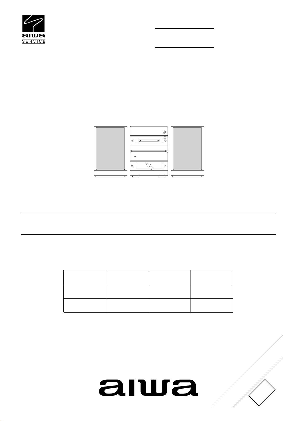
COMPACT DISC STEREO SYSTEM
SYSTEM
XR-M88
XR-M89 RX-LM89 FD-LM89 SX-LM200
This Service Manual is the “Revision Publishing” and replaces “Simple Manual”
(S/M Code No.09-996-333-3T2)
RECEIVER
RX-LM88
.
• BASIC TAPE MECHANISM : TN-708C-128R
• BASIC CD MECHANISM : KSM-620AAA
CD/
CASSETTE
FD-LM88
SPEAKER
SX-LM200
S/M Code No. 09-996-333-3R2
REVISION
DATA
Page 2

TABLE OF CONTENTS
SPECIFICATIONS................................................................................................................................... 3
PROTECTION OF EYES FROM LASER BEAM DURING SERVICING................................................. 4
Precaution to replace Optical block......................................................................................................... 4
MODEL NO. RX-LM88/RX-LM89
ELECTRICAL MAIN PARTS LIST........................................................................................................ 5-7
TRANSISTOR ILLUSTRATION............................................................................................................... 7
FL (13-ST-36GNAK) GRID ASSIGNMENT/ANODE CONNECTION ...................................................... 8
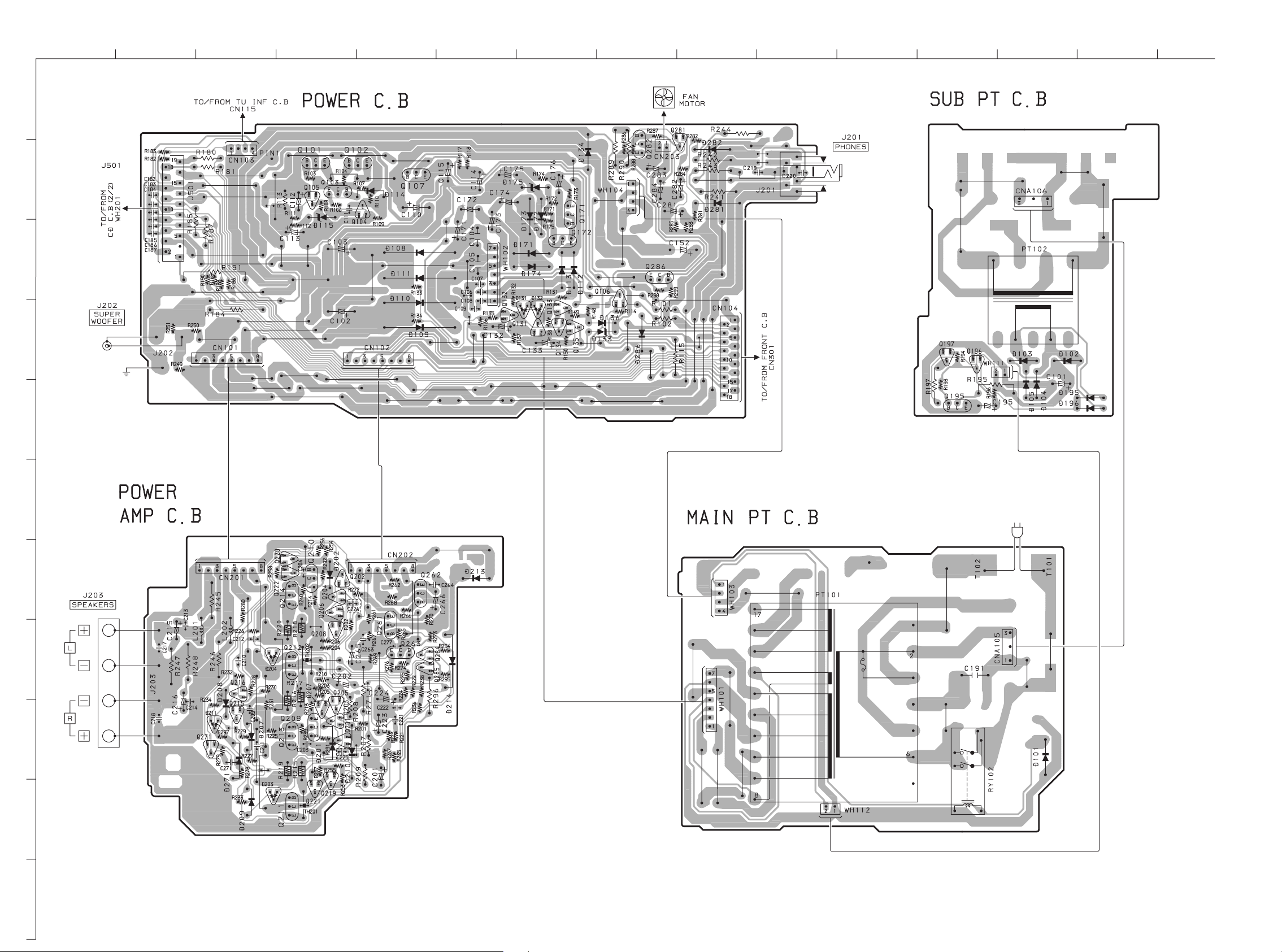
WIRING-1 (POWER AMP)................................................................................................................ 9, 10
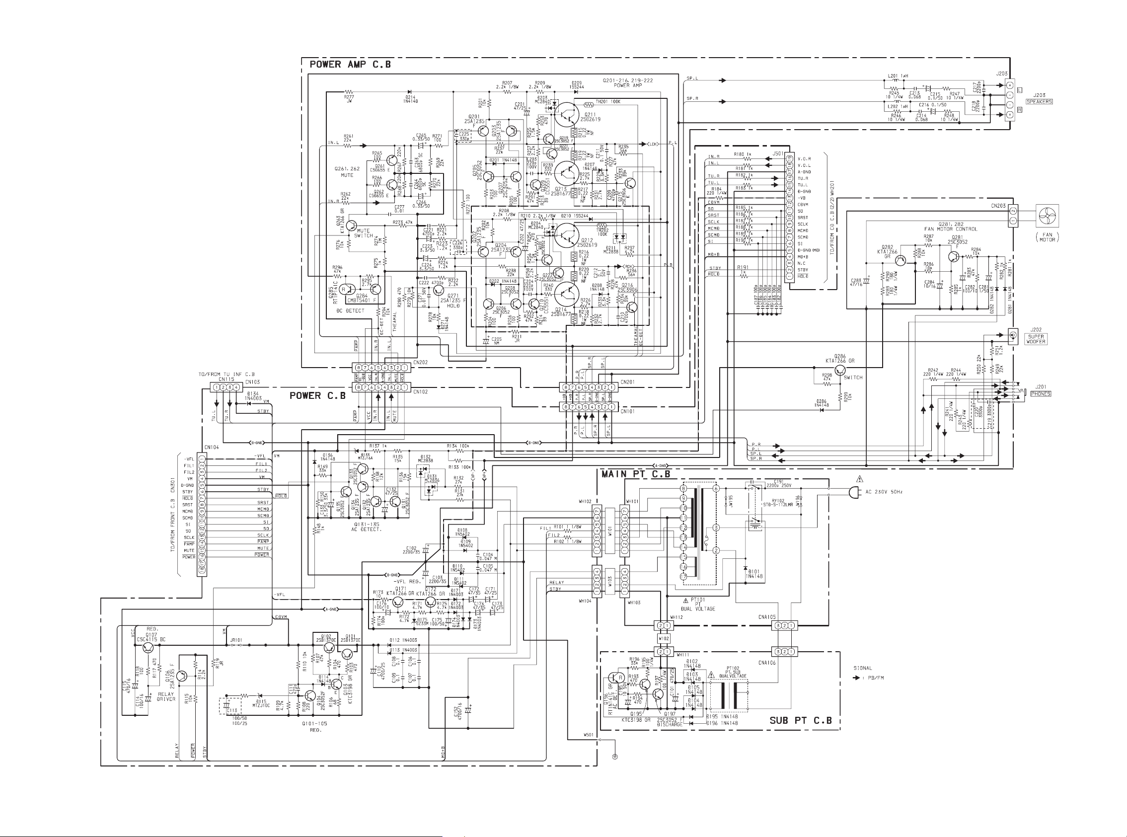
SCHEMATIC DIAGRAM-1 (POWER AMP)..................................................................................... 11, 12
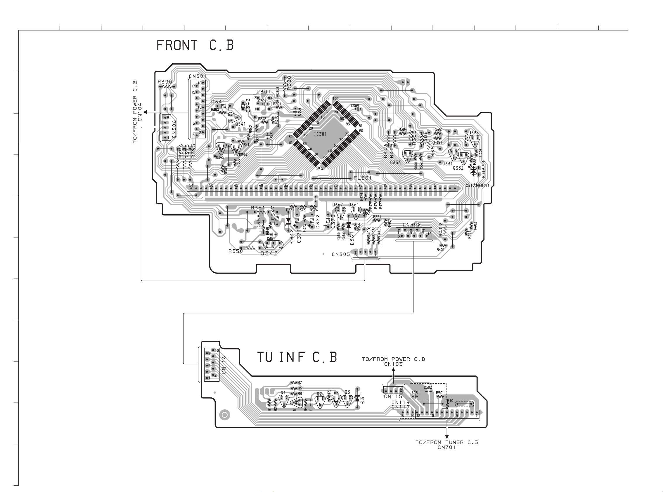
WIRING-2 (FRONT)........................................................................................................................ 13, 14
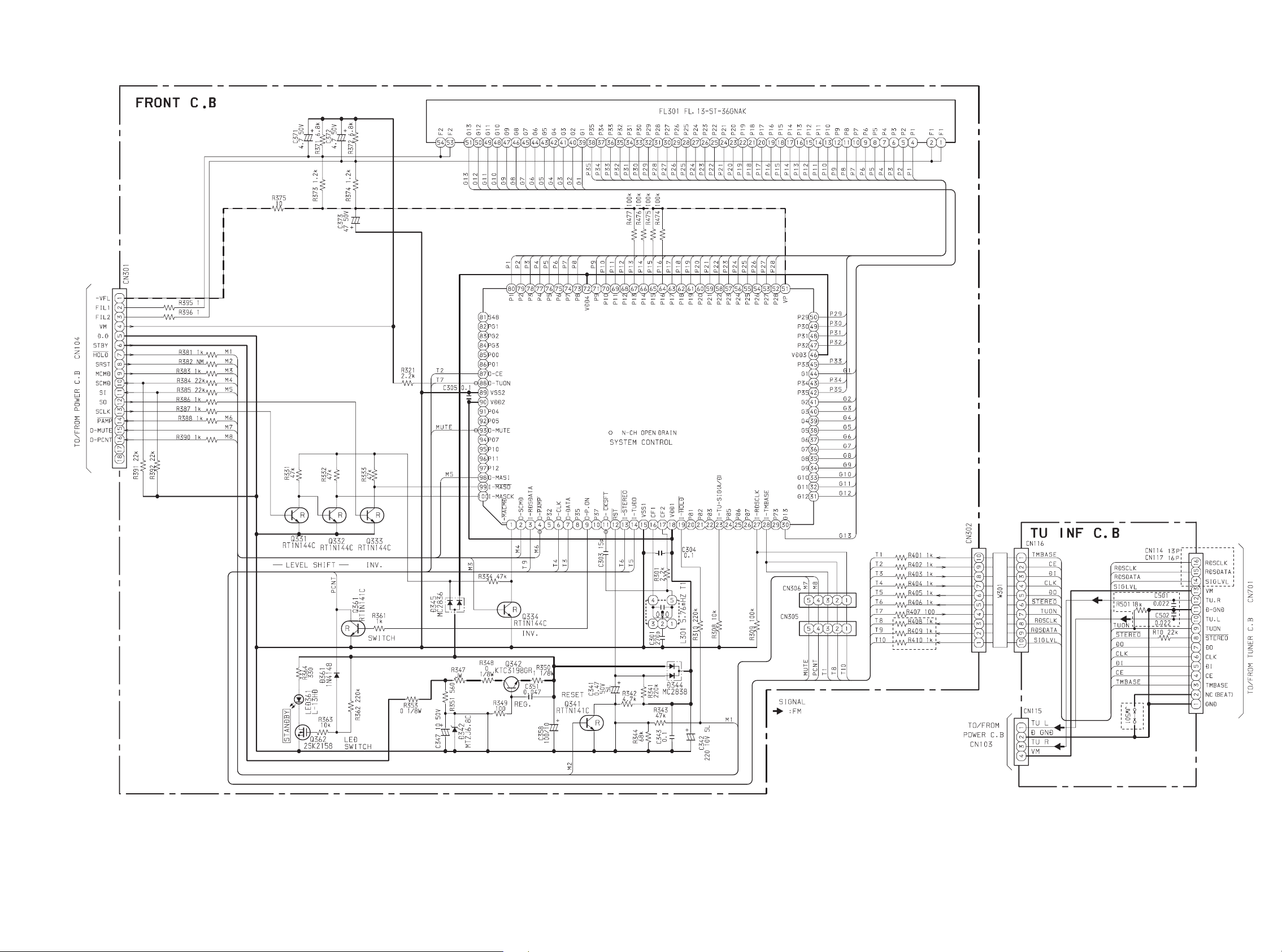
SCHEMATIC DIAGRAM-2 (FRONT)............................................................................................... 15, 16
WIRING-3 (TUNER)........................................................................................................................ 17, 18
SCHEMATIC DIAGRAM-3 (TUNER)............................................................................................... 19, 20
ELECTRICAL ADJUSTMENT/PRACTICAL SERVICE FIGURE .................................................... 21, 22
IC DESCRIPTION........................................................................................................................... 23, 24
IC BLOCK DIAGRAM............................................................................................................................ 25
MECHANICAL EXPLODED VIEW 1/1.................................................................................................. 26
MECHANICAL PARTS LIST 1/1............................................................................................................ 27
MODEL NO. FD-LM88/FD-LM89
DISASSEMBLY INSTRUCTIONS .................................................................................................... 28-32
ELECTRICAL MAIN PARTS LIST.................................................................................................... 33-35
TRANSISTOR ILLUSTRATION............................................................................................................. 36
WIRING-1 (CD) ................................................................................................................................ 37-40
SCHEMATIC DIAGRAM-1 (CD 1/2)................................................................................................ 41, 42
SCHEMATIC DIAGRAM-2 (CD 2/2)................................................................................................ 43, 44
WIRING-2 (TAPE) ........................................................................................................................... 45, 46
WIRING-3 (KEY) ............................................................................................................................. 47, 48
WIRING-4 (FUNC) .......................................................................................................................... 49, 50
SCHEMATIC DIAGRAM-3 (TAPE/FUNC/KEY) ............................................................................... 51, 52
TEST MODE ......................................................................................................................................... 53
ELECTRICAL ADJUSTMENT......................................................................................................... 54, 55
IC DESCRIPTION............................................................................................................................ 56-61
IC BLOCK DIAGRAM............................................................................................................................ 62
MECHANICAL EXPLODED VIEW 1/1.................................................................................................. 63
MECHANICAL PARTS LIST 1/1............................................................................................................ 64
TAPE MECHANISM EXPLODED VIEW 1/1.......................................................................................... 65
TAPE MECHANISM PARTS LIST 1/1 ...................................................................................................66
CD MECHANISM EXPLODED VIEW 1/1 ............................................................................................. 67
CD MECHANISM PARTS LIST 1/1....................................................................................................... 67
MODEL NO. SX-LM200
SPEAKER DISASSEMBLY INSTRUCTIONS ....................................................................................... 68
SPEAKER PARTS LIST 1/1 .................................................................................................................. 69
ACCESSORIES/PACKAGE LIST.......................................................................................................... 69
2
Page 3
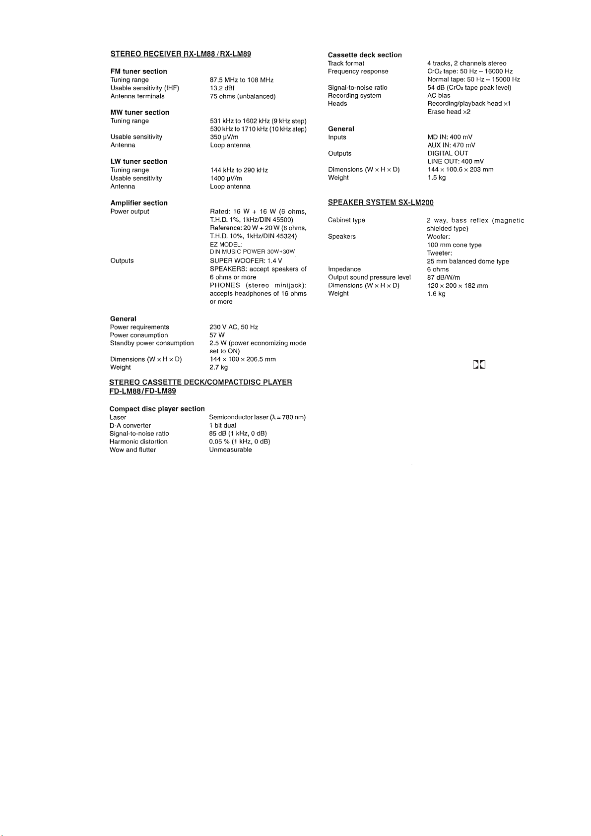
SPECIFICATIONS
Design and specifications are subject to change without
•
notice.
Dolby noise reduction manufactured under license from
•
Dolby Laboratories Licensing Corporation.
“DOLBY” and the double-D symbol
of Dolby Laboratories Licensing Corporation.
The word “BBE” and the “BBE symbol” are trademarks
•
of BBE Sound,Inc.
Under license from BBE Sound,Inc.
are trademarks
3
Page 4
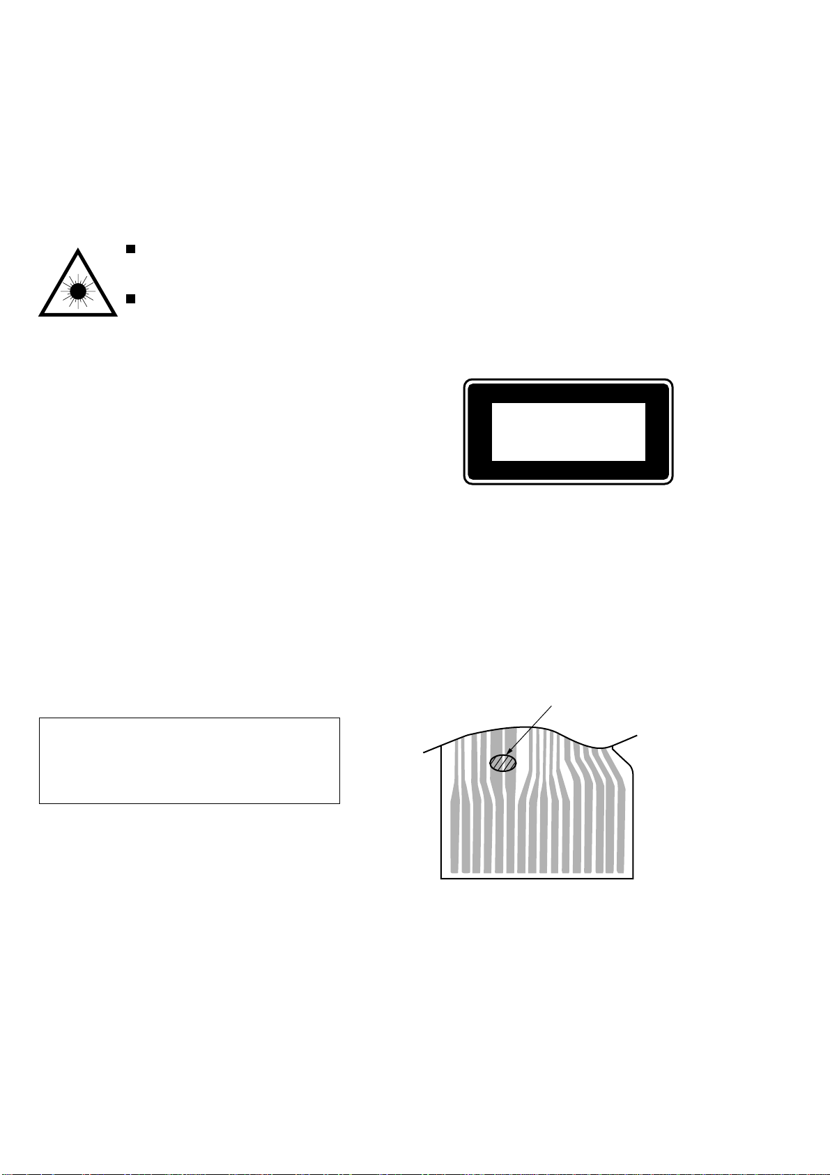
PROTECTION OF EYES FROM LASER BEAM DURING SERVICING
This set employs laser. Therefore, be sure to follow carefully the
instructions below when servicing.
WARNING!
WHEN SERVICING, DO NOT APPROACH THE LASER EXIT
WITH THE EYE TOO CLOSELY. IN CASE IT IS NECESSARY TO
CONFIRM LASER BEAM EMISSION. BE SURE TO OBSERVE
FROM A DISTANCE OF MORE THAN 30cm FROM THE
SURFACE OF THE OBJECTIVE LENS ON THE OPTICAL
PICK-UP BLOCK.
Caution: Invisible laser radiation when
open and interlocks defeated avoid exposure to beam.
Advarsel:Usynling laserståling ved åbning,
når sikkerhedsafbrydere er ude af funktion.
Undgå udsættelse for stråling.
VAROITUS!
Laiteen Käyttäminen muulla kuin tässä käyttöohjeessa mainitulla tavalla saattaa altistaa käyt-täjän turvallisuusluokan 1 ylittävälle näkymättömälle lasersäteilylle.
VARNING!
Om apparaten används på annat sätt än vad som specificeras i
denna bruksanvising, kan användaren utsättas för osynling
laserstrålning, som överskrider gränsen för laserklass 1.
CAUTION
Use of controls or adjustments or performance of procedures
other than those specified herein may result in hazardous
radiation exposure.
ATTENTION
L'utilisation de commandes, réglages ou procédures autres que
ceux spécifiés peut entraîner une dangereuse exposition aux
radiations.
ADVARSEL!
Usynlig laserståling ved åbning, når sikkerhedsafbrydereer ude
af funktion. Undgå udsættelse for stråling.
This Compact Disc player is classified as a CLASS 1 LASER
product.
The CLASS 1 LASER PRODUCT label is located on the rear
exterior.
CLASS 1
KLASSE 1
LUOKAN 1
KLASS 1
LASER PRODUCT
LASER PRODUKT
LASER LAITE
LASER APPARAT
Precaution to replace Optical block
(KSM-620AAA)
Body or clothes electrostatic potential could ruin
laser diode in the optical block. Be sure ground
body and workbench, and use care the clothes
do not touch the diode.
1) After the connection, remove solder shown in
the right figure.
SOLDER
4
Page 5

MODEL NO. RX-LM88
ELECTRICAL MAIN PARTS LIST
REF. NO PART NO. KANRI DESCRIPTION
NO.
IC
87-070-127-110 IC,LC72131 D
87-A20-913-010 IC,LA1837NL
8Z-CL1-627-010 IC,LC866532A-5L31RX
TRANSISTOR
89-213-702-010 TR,2SB1370 (1.8W)
87-026-610-080 TR,KTC3198GR
87-A30-076-080 C-TR,2SC3052F
87-A30-075-080 C-TR,2SA1235F
87-A30-234-080 TR,CSC4115BC
87-026-609-080 TR,KTA1266GR
87-A30-073-080 C-TR,RT1N 141C
87-A30-190-080 TR,CC5551
87-A30-307-010 TR,2SD2619
87-A30-306-010 TR,2SB1677
87-A30-119-040 C-TR,2SC3906K R
87-A30-047-080 TR,CSD655E
87-A30-107-070 C-TR,CMBT5401
87-A30-074-080 C-TR,RT1P 141C
87-A30-071-080 C-TR,RT1N 144C
87-A30-087-080 C-FET,2SK2158
87-A30-072-080 C-TR,RT1P 144C
89-327-143-080 TR,2SC2714 (0.1W)
89-505-434-540 C-FET,2SK543(4/5)
87-A30-086-070 C-TR,CSD1306E
DIODE
87-070-345-080 DIODE,IN4148
87-070-178-090 DIODE,1N5402-BD54
87-070-274-080 DIODE,1N4003 SEM
87-A40-345-080 ZENER,MTZJ10C
87-A40-269-080 C-DIODE,MC2836
87-A40-270-080 C-DIODE,MC2838
87-A40-004-080 ZENER,MTZJ16A
87-A40-312-080 ZENER,DZ33M
87-A40-313-080 C-DIODE,MC 2840
87-A40-488-080 DIODE,1SS244
87-A40-509-080 ZENER,MTZJ6.8C
87-017-149-080 ZENER,HZS6A2L
87-020-465-080 DIODE,1SS133 (110MA)
POWER C.B
C101 87-010-387-080 CAP,E 470-25 SME
C102 87-016-051-090 CAP,E 2200-35 SMG
C103 87-016-051-090 CAP,E 2200-35 SMG
C106 87-010-196-080 CHIP CAPACITOR,0.1-25
C107 87-010-196-080 CHIP CAPACITOR,0.1-25
C108 87-010-196-080 CHIP CAPACITOR,0.1-25
C109 87-010-196-080 CHIP CAPACITOR,0.1-25
C110 87-010-928-090 CAP,E 4700-25 SMG
C111 87-012-140-080 CAP 470P
C113 87-010-247-080 CAP, ELECT 100-50V<K>
C113 87-010-384-080 CAP, ELECT 100-25V<EZ>
C114 87-010-060-080 CAP, ELECT 100-16V
C115 87-010-235-080 CAP,E 470-16 SME
C132 87-010-260-080 CAP, ELECT 47-25V
C133 87-010-403-080 CAP, ELECT 3.3-50V
C151 87-010-196-080 CHIP CAPACITOR,0.1-25
C152 87-A11-174-090 CAP,E 4700-16 M SMG
C171 87-010-260-080 CAP, ELECT 47-25V
C172 87-010-513-080 CAP, ELECT 47-35V
C173 87-010-260-080 CAP, ELECT 47-25V
C174 87-010-260-080 CAP, ELECT 47-25V
C175 87-010-247-080 CAP, ELECT 100-50V
C176 87-010-263-080 CAP, ELECT 100-10V
C182 87-010-322-080 C-CAP,S 100P-50 J CH
REF. NO PART NO. KANRI DESCRIPTION
NO.
C183 87-010-322-080 C-CAP,S 100P-50 J CH
C184 87-010-322-080 C-CAP,S 100P-50 J CH
C185 87-010-322-080 C-CAP,S 100P-50 J CH
C186 87-010-322-080 C-CAP,S 100P-50 J CH
C187 87-010-322-080 C-CAP,S 100P-50 J CH
C191 87-A10-479-080 CAP,CER 2200P-250 M E KH
C195 87-010-405-080 CAP, ELECT 10-50V<EZ>
C195 87-010-405-010 CAP, ELECT 10-50V<K>
C281 87-010-401-080 CAP, ELECT 1-50V
C282 87-010-263-080 CAP, ELECT 100-10V
C283 87-010-380-080 CAP, ELECT 47-16V
C284 87-010-405-080 CAP, ELECT 10-50V
CN101 87-A60-813-010 CONN,8P H BLK TAC-L8X
CN102 87-A60-813-010 CONN,8P H BLK TAC-L8X
CN104 87-A60-770-010 CONN,18P B TMC-D(X)
CN203 87-A60-109-010 CONN,2P V S2M-2W
CN301 87-A60-778-010 CONN,18P B TMC-D(P)
CN302 87-A60-058-010 CONN,10P V 9604S-10C
CN305 8Z-CL1-665-010 CONN ASSY,5P FR
J201 87-A60-420-010 JACK,3.5 ST (MSC)
J202 87-099-801-010 JACK,PIN 1P BLK
J501 87-A60-782-010 CONN,19P H FG
W101 8Z-CL1-656-010 F-CABLE,7P 2.5 150MM PWR
W102 8Z-CL1-654-010 F-CABLE,2P 2.5 170MM SUBPT
W103 8Z-CL1-655-010 F-CABLE,4P 2.5 100MM PWR
WH102 87-A90-460-010 HLDR,WIRE 2.5-7P
FRONT C.B
C301 87-012-145-080 CAP, CHIP S 270P CH
C303 87-010-312-080 C-CAP,S 15P-50 CH
C304 87-015-785-080 CHIP CAPACITOR, 0.1FZ-25Z
C305 87-010-196-080 CHIP CAPACITOR,0.1-25
C341 87-010-493-080 CAP,E 0.47-50 GAS
C342 87-A10-189-040 CAP,E 220-10
C343 87-010-196-080 CHIP CAPACITOR,0.1-25
C347 87-010-405-080 CAP, ELECT 10-50V
C351 87-010-194-080 CAP, CHIP 0.047
C352 87-010-194-080 CAP, CHIP 0.047
C358 87-010-263-080 CAP, ELECT 100-10V
C371 87-010-404-080 CAP, ELECT 4.7-50V
C372 87-010-404-080 CAP, ELECT 4.7-50V
C373 87-010-408-080 CAP, ELECT 47-50V
FL301 8Z-CL1-630-010 FL,13-ST-36GNAK
HL301 8Z-CL1-204-010 HLDR,FL
L301 87-A50-052-010 COIL,CLOCK 5.76MHZ T1
LED361 87-A40-568-010 LED,L-13HD RED
POWER AMP C.B
C201 87-010-260-080 CAP, ELECT 47-25V
C202 87-010-260-080 CAP, ELECT 47-25V
C203 87-A10-946-080 C-CAP,S 220P-100 J CH
C204 87-A10-946-080 C-CAP,S 220P-100 J CH
C209 87-010-186-080 CAP,CHIP 4700P
C210 87-010-186-080 CAP,CHIP 4700P
C211 87-012-368-080 C-CAP,S 0.1-50 F
C212 87-012-368-080 C-CAP,S 0.1-50 F
C213 87-010-195-080 C-CAP,S 0.068-25 F
C214 87-010-195-080 C-CAP,S 0.068-25 F
C215 87-010-544-080 CAP, ELECT 0.1-50V
C216 87-010-544-080 CAP, ELECT 0.1-50V
C217 87-010-182-080 C-CAP,S 2200P-50 B
C218 87-010-182-080 C-CAP,S 2200P-50 B
C219 87-010-184-080 C-CAP,S 3300P-50 B<EZ>
C220 87-010-184-080 C-CAP,S 3300P-50 B<EZ>
C221 87-010-186-080 CAP,CHIP 4700P
C222 87-010-186-080 CAP,CHIP 4700P
C223 87-010-403-080 CAP, ELECT 3.3-50V
C224 87-010-403-080 CAP, ELECT 3.3-50V
5
Page 6

REF. NO PART NO. KANRI DESCRIPTION
C225 87-012-157-080 C-CAP,S 330P-50 J CH<EZ>
C226 87-012-157-080 C-CAP,S 330P-50 J CH<EZ>
C265 87-010-546-080 CAP, ELECT 0.33-50V
C266 87-010-546-080 CAP, ELECT 0.33-50V
C271 87-015-819-080 CAPACITOR,0.01
C277 87-010-197-080 CAP, CHIP 0.01 DM
CN201 87-A60-812-010 CONN,8P V BLK TAC-L8P
CN202 87-A60-812-010 CONN,8P V BLK TAC-L8P
J203 87-YP6-608-010 TERMINAL,SPKR 4P
L201 87-003-383-010 COIL,1UH-S
L202 87-003-383-010 COIL,1UH-S
R215 87-A00-258-080 RES,M/F 0.22-1W J
R216 87-A00-258-080 RES,M/F 0.22-1W J
R217 87-A00-258-080 RES,M/F 0.22-1W J
R218 87-A00-258-080 RES,M/F 0.22-1W J
R219 87-A00-258-080 RES,M/F 0.22-1W J
R220 87-A00-258-080 RES,M/F 0.22-1W J
TH201 87-A91-042-080 C-THMS,100K 55001
TH202 87-A91-042-080 C-THMS,100K 55001
MAIN PT C.B
!
PR151 87-A90-094-080 PROTECTOR,4A 491SERIES 60V
!
PT101 8Z-CL1-623-010 PT,E
RY102 87-A90-976-010 RELAY,AC12V SDT-S-112LMR
!
T101 87-A60-317-010 TERMINAL, 1P MSC
!
T102 87-A60-317-010 TERMINAL, 1P MSC
WH101 87-A90-460-010 HLDR,WIRE 2.5-7P
SUB PT C.B
!
PT102 8Z-CL1-673-010 PT,SUB ZCL-1(E)
TU INF C.B
C501 87-010-189-080 C-CAP,S 8200P-50 B<EZ>
C502 87-010-189-080 C-CAP,S 8200P-50 B<EZ>
CN114 87-099-570-010 CONN,13P TUC-P13P-B1<K>
CN115 87-A60-114-010 CONN,4P H S2M-4WR
CN116 87-A60-077-010 CONN,10P H 9604S-10F
CN117 87-A60-189-010 CONN,16P V TUC-P16P-B1<EZ>
TUNER C.B
C701 87-010-381-080 CAP, ELECT 330-16V
C702 87-010-404-080 CAP, ELECT 4.7-50V
C703 87-012-286-080 CAP, U 0.01-25
C704 87-012-286-080 CAP, U 0.01-25
C709 87-012-195-080 C-CAP,U 100P-50CH
C711 87-010-260-080 CAP, ELECT 47-25V
C712 87-010-831-080 C-CAP,U,0.1-16F
C713 87-012-286-080 CAP, U 0.01-25
C714 87-012-286-080 CAP, U 0.01-25
C715 87-012-195-080 C-CAP,U 100P-50CH
C717 87-012-286-080 CAP, U 0.01-25
C719 87-012-286-080 CAP, U 0.01-25
C720 87-012-195-080 C-CAP,U 100P-50CH
C721 87-012-176-080 CAP 15P
C722 87-012-176-080 CAP 15P
C723 87-012-274-080 CHIP CAP,U 1000P-50B
C725 87-018-131-080 CAP, CER 1000P-50V
C727 87-010-196-080 CHIP CAPACITOR,0.1-25
C728 87-010-248-080 CAP, ELECT 220-10V
C729 87-012-274-080 CHIP CAP,U 1000P-50B
C731 87-012-286-080 CAP, U 0.01-25
C733 87-012-280-080 CAP, U 3300P-50
C734 87-012-280-080 CAP, U 3300P-50
C752 87-012-282-080 CAP, U 4700P-50
C753 87-012-195-080 C-CAP,U 100P-50CH
NO.
REF. NO PART NO. KANRI DESCRIPTION
NO.
C755 87-012-286-080 CAP, U 0.01-25
C756 87-012-286-080 CAP, U 0.01-25
C757 87-012-188-080 C-CAP,U 47P-50 CH
C758 87-012-167-080 C-CAP,U 5P-50 CH
C761 87-010-196-080 CHIP CAPACITOR,0.1-25
C762 87-012-286-080 CAP, U 0.01-25
C763 87-010-829-080 CAP, U 0.047-16
C765 87-012-286-080 CAP, U 0.01-25
C766 87-010-197-080 CAP, CHIP 0.01 DM
C768 87-012-286-080 CAP, U 0.01-25
C769 87-010-260-080 CAP, ELECT 47-25V
C770 87-010-829-080 CAP, U 0.047-16
C771 87-010-383-080 CAP, ELECT 33-25V
C772 87-010-829-080 CAP, U 0.047-16
C773 87-010-196-080 CHIP CAPACITOR,0.1-25
C774 87-010-263-080 CAP, ELECT 100-10V
C775 87-010-404-080 CAP, ELECT 4.7-50V
C776 87-012-286-080 CAP, U 0.01-25
C777 87-010-493-080 CAP,E 0.47-50 GAS
C778 87-010-401-080 CAP, ELECT 1-50V
C779 87-010-401-080 CAP, ELECT 1-50V
C780 87-010-196-080 CHIP CAPACITOR,0.1-25
C781 87-010-405-080 CAP, ELECT 10-50V
C782 87-010-405-080 CAP, ELECT 10-50V
C783 87-012-286-080 CAP, U 0.01-25
C784 87-012-286-080 CAP, U 0.01-25
C785 87-010-405-080 CAP, ELECT 10-50V
C786 87-010-405-080 CAP, ELECT 10-50V
C787 87-012-275-080 C-CAP,U 1200P-50 B
C788 87-012-275-080 C-CAP,U 1200P-50 B
C789 87-012-275-080 C-CAP,U 1200P-50 B
C790 87-012-275-080 C-CAP,U 1200P-50 B
C791 87-010-405-080 CAP, ELECT 10-50V
C793 87-012-273-080 C-CAP,U 820P-50 B
C794 87-010-406-080 CAP, ELECT 22-50
C795 87-010-596-080 CAP, S 0.047-16
C796 87-010-403-080 CAP, ELECT 3.3-50V
C797 87-012-276-080 CAP, CHIP SS 1500 PBK
C798 87-012-276-080 CAP, CHIP SS 1500 PBK
C799 87-010-829-080 CAP, U 0.047-16
C812 87-012-286-080 CAP, U 0.01-25
C814 87-012-286-080 CAP, U 0.01-25
C820 87-010-260-080 CAP, ELECT 47-25V
C821 87-012-286-080 CAP, U 0.01-25
C822 87-012-286-080 CAP, U 0.01-25
C823 87-012-286-080 CAP, U 0.01-25
C828 87-010-196-080 CHIP CAPACITOR,0.1-25
C829 87-010-196-080 CHIP CAPACITOR,0.1-25
C859 87-012-286-080 CAP, U 0.01-25<EZ>
C861 87-012-199-080 CAP 220P<EZ>
C862 87-012-199-080 CAP 220P<EZ>
C863 87-012-270-080 CAP, U 470P-50<EZ>
C864 87-010-405-080 CAP, ELECT 10-50V<EZ>
C865 87-010-196-080 CHIP CAPACITOR,0.1-25<EZ>
C866 87-010-405-080 CAP, ELECT 10-50V<EZ>
C867 87-012-286-080 CAP, U 0.01-25<EZ>
C868 87-012-184-080 C-CAP,U 33P-50 CH<EZ>
C869 87-012-180-080 C-CAP,U 22P-50 CH<EZ>
C940 87-012-286-080 CAP, U 0.01-25
C942 87-012-168-080 C-CAP,U 6P-50 CH
C947 87-012-286-080 CAP, U 0.01-25
C949 87-A10-039-080 C-CAP,U 470P-50 J CH
C952 87-012-286-080 CAP, U 0.01-25
C958 87-010-197-080 CAP, CHIP 0.01 DM
C959 87-010-831-080 C-CAP,U,0.1-16F
C960 87-010-196-080 CHIP CAPACITOR,0.1-25
C962 87-010-401-080 CAP, ELECT 1-50V
CF801 87-008-423-010 CERAMIC FILTER, SFE10.7
CF802 82-785-747-010 CF MS2 GHY R
CN701 87-A60-700-010 CONN,13P H GRY TUC-P13X-C1<K>
6
Page 7
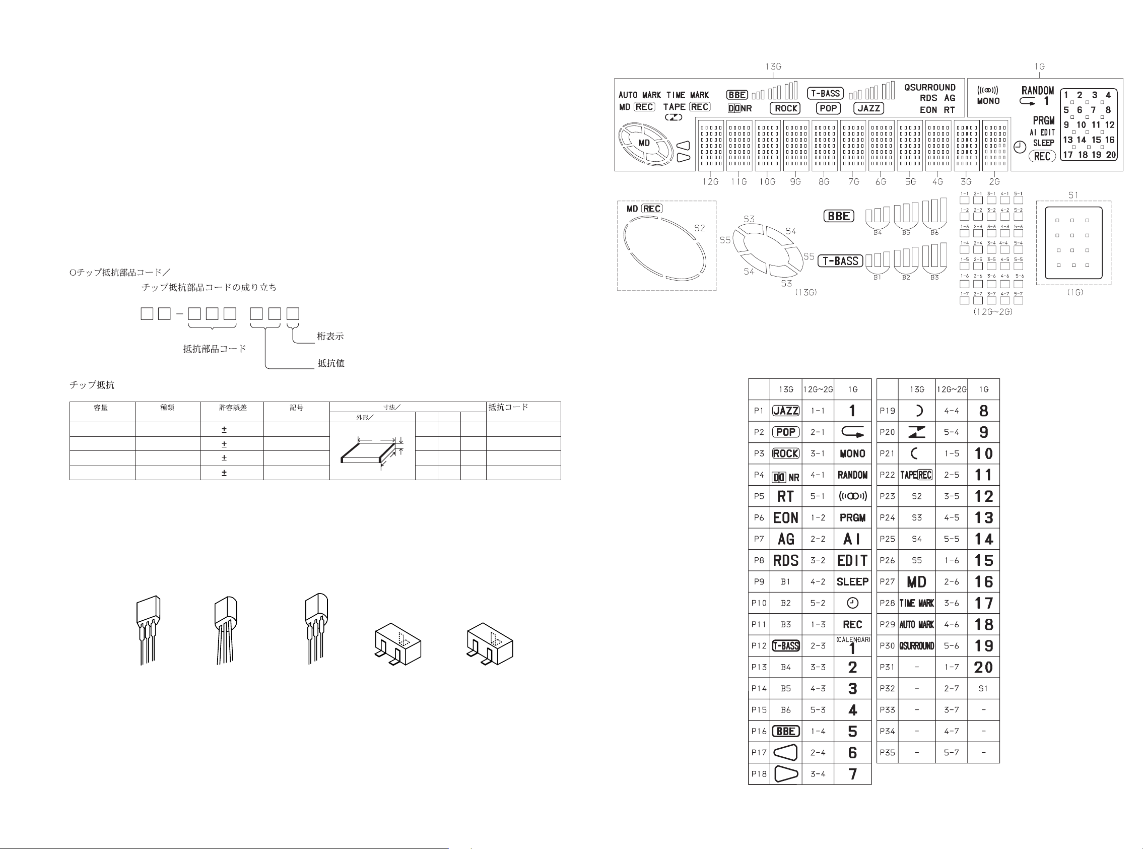
FL (13-ST-36GNAK) GRID ASSIGNMENT/ANODE CONNECTION
GRID ASSIGNMENT
REF. NO PART NO. KANRI DESCRIPTION
NO.
C962 87-010-401-080 CAP, ELECT 1-50V
CF801 87-008-423-010 CERAMIC FILTER, SFE10.7
CF802 82-785-747-010 CF MS2 GHY R
CN701 87-A60-700-010 CONN,13P H GRY TUC-P13X-C1
CN701 87-A60-650-010 CONN,16P H GRY TUC-P16X-C1<EZ>
FFE801 A8-6ZA-191-130 6ZA-1 FEENM
J801 87-033-241-010 TERMINAL,ANT AJ-2039
L771 87-A50-266-010 COIL,FM DET-2N(TOK)
L772 87-A91-110-010 FLTR,PCFJZH-450 (TOK)
L781 87-005-847-080 COIL,2.2UH(CECS)
• Regarding connectors, they are not stocked as they are not the initial order items.
The connectors are available after they are supplied from connector manufacturers upon the order is received.
CHIP RESISTOR PART CODE
REF. NO PART NO. KANRI DESCRIPTION
NO.
L791 87-A50-027-010 COIL,1 POLE MPX(TOK)
L792 87-A50-027-010 COIL,1 POLE MPX(TOK)
L832 87-005-847-080 COIL,2.2UH(CECS)
L851 87-005-847-080 COIL,2.2UH(CECS)<EZ>
L941 87-A50-020-010 COIL,ANT LW(COI)
L942 87-A50-019-010 COIL,OSC LW(COI)
L981 8Z-ZA1-665-010 COIL,AM PACK 2(TOK)
TC942 87-011-164-010 CAPACITOR,TRIMMER 30P
X721 87-A70-061-010 VIB,XTAL 4.500MHZ CSA-309
X851 87-A70-091-010 VIB,XTAL 4.332MHZ CSA-309<EZ>
Chip Resistor Part Coding
88
A
Resistor Code
Figure
Value of resistor
ANODE CONNECTION
Chip resistor
Wattage Type Tolerance
1/16W 1005 5% CJ
1/16W
1/10W
1/8W
1608
2125
3216
5%
5%
5%
TRANSISTOR ILLUSTRATION
ECB ECBECB
2SA933 2SA1235
2SA1318
2SC2001
CSD655E
CSD1489B
KTC3198
Symbol
CJ
CJ
CJ
KTA1266
Dimensions (mm)
Form
L
t
W
C
B
E
DTA144TK
DTC114TK
RT1N144C
0.55
Resistor Code
108
118
128
LW t
1.0 0.5 0.35 104
1.6 0.8 0.45
2 1.25 0.45
3.2
1.6
D
G
S
2SK2158
: A
: A
87
Page 8
WIRING-1 (POWER AMP)
1
A
B
C
D
234567
8
9
10
11 12 13
14
E
F
AC230V 50Hz
G
EZ
MODEL
H
I
EZ
MODEL
J
K
109
Page 9
SCHEMATIC DIAGRAM-1 (POWER AMP)
EZ MODEL
EZ MODEL
EZ MODEL
K MODEL:
EZ MODEL:
1211
Page 10
WIRING-2 (FRONT)
1
A
B
C
D
234567
8
9
10
11 12 13
14
E
EZ MODEL
F
G
H
I
EZ MODEL
K MODEL:
EZ MODEL:
EZ
MODEL
K MODEL
J
K
1413
Page 11
SCHEMATIC DIAGRAM-2 (FRONT)
IC301
LC866532A-5L31RX
EZ MODEL
EZ
MODEL
K MODEL
K:
EZ:
1615
Page 12
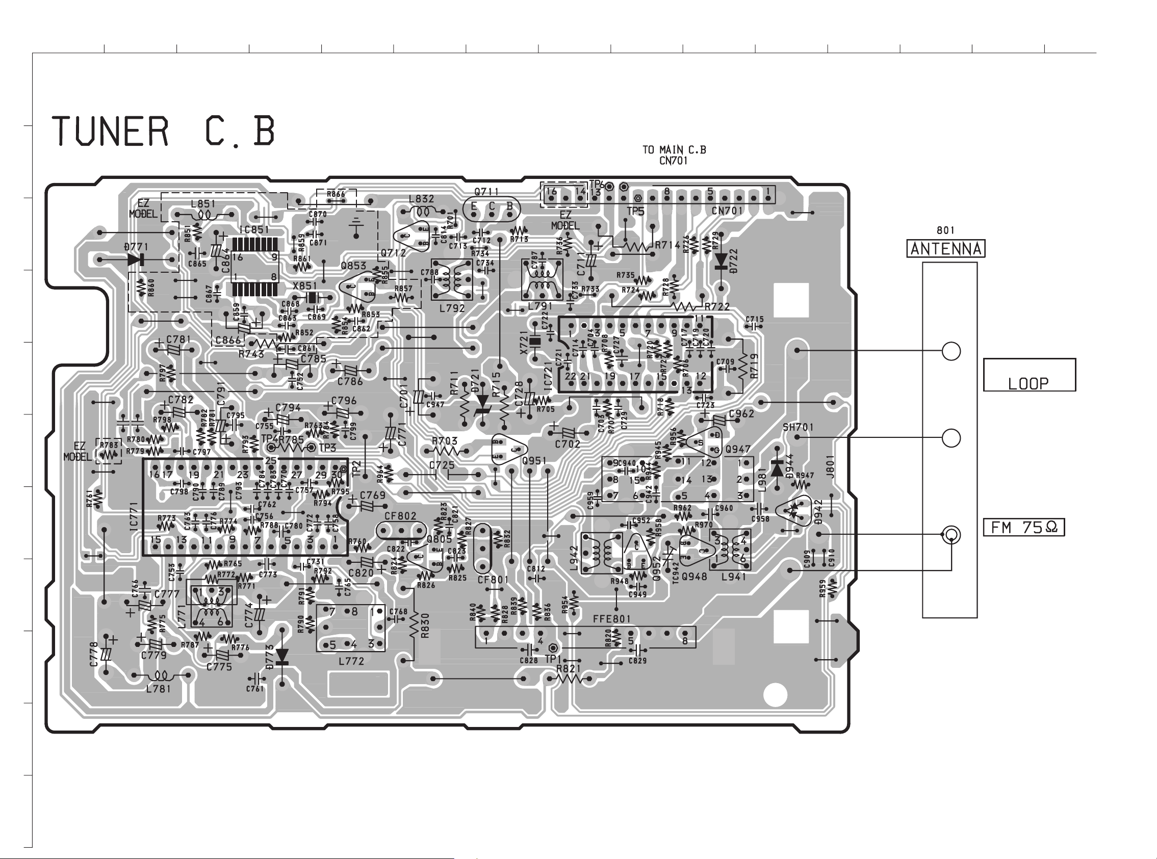
WIRING-3 (TUNER)
1
A
B
234567
8
9
10
11 12 13
14
C
D
E
F
G
J
MW / LW
H
I
J
K
1817
Page 13
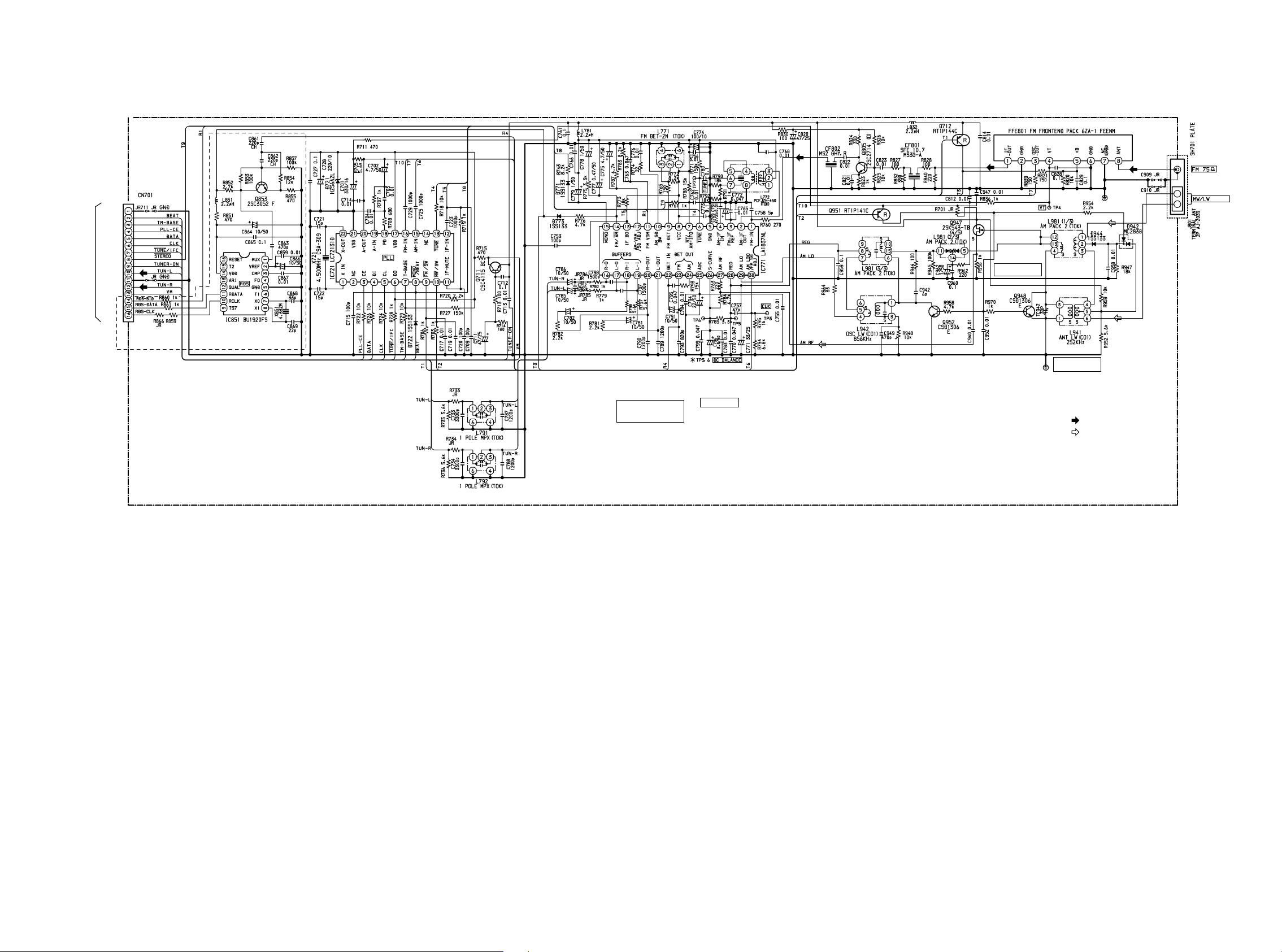
SCHEMATIC DIAGRAM-3 (TUNER)
TO/FROM MAINC.B CN701
BUFFER
AMP
EZ MODEL
TU+B
SW
L771
DC BALLANCE /
MONO DISTORTION
ADJ
L772
MW IF ADJ
BAND SW
BAND
SW
BAND
SW
AMP
MW TRACKING
ADJ
LW TRACKING
ADJ
L941,TC942
SIGNAL
: FM
:MW/LW
LOOP
TUNER C.B
2019
Page 14
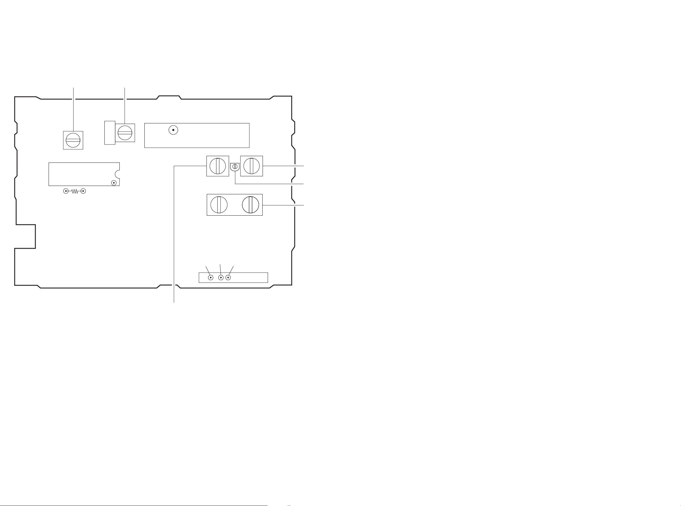
ELECTRICAL ADJUSTMENT 2/2
8
L771
TP4
IC771
TP3
R785
30
TP2
3
L772
TP1
4
L942
L981
FFE801
TUNER C.B
L941TC942
7
7
4
< TUNER SECTION >
1. Clock Frequency Check
Settings: • Test point: TP2 (CLK IC770 pin30)
Method: Set to MW 1602kHz and check that the test
point becomes 2052kHz±45Hz (EZ).
2. MW VT Check
Settings: • Test point: TP1 (VT)
Method: Set to MW 1602kHz and check that the test
point is less than 8.0V.
Then set to MW 531kHz and check that the
test point is more than 0.6V.
3. MW IF Adjustment
Settings: • Test point: TP5, TP6
L772 .............................................. 450kHz
4. MW Tracking Adjustment
Settings: • Test point: TP5, TP6
• Adjustment location: L981
Method: Set to MW 999kHz and adjust L981 so that the
test point becomes maximum.
5. FM VT Check
Settings: • Test point: TP1 (VT)
Method: Set to FM 87.5MHz, 108.0MHz and check that
the test point is more than 0.5V (87.5MHz) and
less than 8.0V (108.0MHz).
PRACTICAL SERVICE FIGURE
< TUNER SECTION >
< FM SECTION >
IHF Sensitiviy: Less than 13dB
(THD 3%) (at 108.0/98.0MHz)
Less than 14dB
(at 98.0MHz)
Distortion: Less than 1.2% (98.0MHz)
Stereo separation: More than 12dB (98.0MHz)
Intermediate frequency: 10.7MHz
< MW SECTION >
Sensitivity: Less than 60dB (at 600kHz)
(S/N 20dB) Less than 58dB
(at 1000/1400kHz)
Distortion: Less than 1.5%
(at 1000kHz)
< LW SECTION >
Sensitivity: Less than 70dB (at 144kHz)
Less than 68dB (at 198kHz)
Less than 66dB (at 290kHz)
6
TP6
GND
12 11 10
TP5
6. LW VT Adjustment
Settings: • Test point: TP2 (VT)
• Adjustment location: L942
Method: Set to LW 144kHz and adjust L942 so that the
test point becomes 1.3V±0.05V.
Then set to LW 290kHz and check that the test
point is less than 8.0V.
CN701
7. LW Tracking Adjustment
Settings: • Test point: TP5, TP6
• Adjustment location:
L941 .............................................. 144kHz
TC942 ...........................................290kHz
Method: Set up TC942 to center before adjustment.
The level at 144kHz is adjusted to MAX by
L941. Then the level at 290kHz is adjusted to
MAX by TC942.
8. DC Balance/Mono Distortion Adjustment
Settings: • Test point: TP3, TP4
• Adjustment location: L771
• Input level: 54dB
Method: Set to FM 98.0MHz and adjust L771 so that
the voltage between TP3 and TP4 becomes
0V±0.04V.
Next, check that the distortion is less than
1.3%.
2221
Page 15

IC DESCRIPTION
IC, LC866532A-5L31RX
Pin No. Pin Name I/O Description
1
2
3
4
5
6
7
8
9
10
11
12
13
14
15
16
17
18
19
20-22
23
24-26
________________
I-MACMD
O-SCMD
1-RDSDATA
___________
O-PAMP
P32
O-CLK
O-DATA
P35
O-P.ON
P37
_____________
O-CKSFT
________
RST
________________
I-STEREO
I-TUDO
VSS1
CF1
CF2
VDD1
____________
I-HOLD
P81-P83
I-TU-SIG
P85-P87
I
Command input from master microprocessor.
O
Serial data output to master microprocessor.
I
RDS data input.
O
Power supply control output (power supply ON/OFF of POWER AMP).
—
NC.
O
Connected to TUNER PLL IC LC72131 pin-5 CL.
O
Connected to TUNER PLL IC LC72131 pin-4 DI.
—
NC.
O
Power save mode control output
—
NC.
O
Clock shift output. “L” at clock shift.
I
Microprocessor reset.
I
TUNER, STEREO detection.
I
Connected to TUNER PLL IC LC72131 pin-6 D0.
—
GND.
I
5.76 MHz. Connected to oscillator.
O
—
Microprocessor power supply (µ-com 5V).
I
Hold state detection. (Ignored by slave microprocessor)
—
NC.
I
RDS signal level AD value input (A/D).
—
NC.
27
28
29
30-41
42, 43
44
45
46
47-50
51
52-71
72
73-80
81
82-84
85, 86
87
88
I-RDSCLK
I-TMBASE
P73
G13-G2
P35, P34
G1
P33
VDD3
P32-P29
VP
P28-P9
VDD4
P8-P1
S48
PG1-PG3
P00, P01
O-CE
O-TUON
I
RDS CLK input.
I
Reference clock input for watch. Connected to PLL ICLC72131 pin-7.
—
NC.
O
FL tube grid output. (13G-2G).
O
FL tube anode output. (P35, P34).
O
FL tube grid output. (1G).
O
FL tube anode output. (P33).
—
Microprocessor power supply. (µ-com 5V).
O
FL tube anode output. (P32-P29).
—
Connected to minus power supply -VFL for FL.
O
FL tube anode output. (P28-P9).
—
Microprocessor power supply. (µ-com 5V).
O
FL tube anode output. (P8-P1).
—
—
NC.
—
O
Connected to TUNER PLL IC LC72131pin-3 CE.
O
TUNER power supply. ON/OFF output.
89
VSS2
—
GND.
23
Page 16

Pin No. Pin Name I/O Description
90
91, 92
93
VDD2
P04, P05
O-MUTE
—
—
Microprocessor power supply. (µ-com 5V).
NC.
O
Main mute output.
94
95-97
98
99
100
P07
P10-12
O-MASI
____________
I-MASO
I-MACLK
—
—
NC.
O
Serial data output to master microprocessor.
I
Serial data input from master microprocessor.
I
Transfer clock input from master microprocessor.
24
Page 17

IC BLOCK DIAGRAM
IC, BU1920FS
IC, LA1837
IC, LC72131
25
Page 18

MECHANICAL EXPLODED VIEW 1/1
P.C.B
3
2
F
1
FL
E
F
C
E
HT-SINK,SUB
8
7
20
HT-SINK,MAIN ASSY
A
G
A
5
4
B
13
6
B
B
C
19
14
P.C.B
SHLD-PLATE PT
G
J
P.C.B
G
P.C.B
10
A
11
I
SHLD-PLATE
SUB.PT
18
P.C.B
A
15
B
B
C
B
H
H
16
12
P.C.B
P.C.B
9
CHAS,MAIN
17
26
Page 19

MECHANICAL PARTS LIST 1/1
REF. NO PART NO. KANRI DESCRIPTION
1 8Z-CL1-056-010 WINDOW,DISP EX<88<K>>
1 8Z-CL1-055-010 WINDOW,DISP EZ<89<EZ>>
2 8Z-CLB-013-010 PANEL,RX CS<88<K>>
2 8Z-CLB-015-010 PANEL,RX CS EZ<89<EZ>>
3 8Z-CL1-001-010 CABI,FR RX
4 8Z-CL1-204-010 HLDR,FL
5 88-910-131-110 FF-CABLE,10P 1.25
6 8Z-CL1-003-010 CABI,TOP RX
7 8Z-CL1-655-010 F-CABLE,4P 2.5 100MM PWR
8 8Z-CL1-656-010 F-CABLE,7P 2.5 150MM PWR
9 8Z-CL1-213-010 COVER, PWB AC
10 87-A90-193-010 HLDR,CV100 (B)
11 8Z-CL1-203-010 HLDR,SUB PT
12 8Z-CL1-663-010 FAN,MF40D-12-200MM
13 8Z-CLB-073-010 PANEL,REAR RX CS EZ<89<EZ>>
13 8Z-CLB-071-010 PANEL,REAR RX CS K<88<K>>
14 87-A90-460-010 HLDR,WIRE 2.5-7P
15 87-085-185-010 BUSHING, AC CORD (E)
!
16 87-A80-092-010 AC CORD ASSY,E BLK SUN
!
16 87-A80-007-110 AC CORD ASSY,K BLK<88<K>>
NO.
FAI<89<EZ>>
REF. NO PART NO. KANRI DESCRIPTION
17 81-669-025-010 FOOT, H11
18 8Z-CL1-654-010 F-CABLE,2P 2.5 170MM SUBPT
!
19 8Z-CL1-623-010 PT,E
20 86-NF6-211-010 HLDR,IC T1.6
A 87-067-703-010 TAPPING SCREW, BVT2+3-10
B 87-744-095-410 VT2+3-8 W/O SLOT CR2
C 87-B10-068-010 UTT2+3-6 W/O SLOT CR
D 8Z-CL1-034-010 S-SCREW,ZCL1
E 87-591-094-010 QIT+3-6 GOLD
F 87-067-761-010 TAPPING SCREW, BVT2+3-10
G 87-067-585-010 TAPPING SCREW, BVTT+4-6
H 87-751-095-410 VT2+3-8
I 87-067-584-010 TAPPING SCREW, BVT2+3-6
J 87-067-981-010 BVT2+3-6 BLK
NO.
COLOR NAME TABLE
Basic color symbol Color Basic color symbol Color Basic color symbol Color
B Black C Cream D Orange
G Green H Gray L Blue
LT Transparent Blue N Gold P Pink
R Red S Silver ST Titan Silver
T Brown V Violet W White
WT Transparent White Y Yellow YT Transparent Yellow
LM Metallic Blue LL Light Blue GT Transparent Green
LD Dark Blue DT Transparent Orange
27
Page 20

MODEL NO. FD-LM88
DISASSEMBLY INSTRUCTIONS
1. Remove the two screws.
1
2. Remove the two screws.
28
2
Page 21

3. Remove the eight screws and remove the PANEL, REAR FD.
3
4. While moving up the rear of the PANEL, TOP, remove the PANEL, TOP by pulling it to the front.
29
Page 22

5. Remove the FFC and cord. Be careful that the FFC especially cannot be removed easily.
6. Remove the screws.
6
30
Page 23

7. Remove the two FFCs.
8. Remove the claw and remove the CABI FRFD together with the entire front board.
31
Page 24

9. While moving up the CD board and the function board, remove the CD board and the function board. You can locate the
mechanism deck.
32
Page 25

ELECTRICAL MAIN PARTS LIST
REF. NO PART NO. KANRI DESCRIPTION
NO.
IC
87-A20-446-010 C-IC,LA9241ML
87-A20-459-010 C-IC,LC78622ED
87-A20-445-010 IC,BA5936
8Z-CLB-621-010 C-IC,LC866560-5M02FD
87-A20-455-010 IC,HA12211
87-001-982-010 IC,TA7291S
87-A21-111-040 C-IC,M62495FP
87-A21-022-040 C-IC,BA3880FS
87-A21-103-040 C-IC,MM1454XFBE
87-017-888-080 IC,NJM4558MD
87-A20-914-010 IC,SPS-442-1-F
TRANSISTOR
87-026-463-080 TR,2SA933S (0.3W)
89-113-184-080 TR,2SA1318T
87-026-297-080 TR,DTA144TK
87-026-239-080 TR,DTC114TK (0.2W)
87-A30-047-080 TR,CSD655E
87-A30-075-080 C-TR,2SA1235F
87-026-610-080 TR,KTC3198GR
87-A30-083-080 TR,CSD1489B
87-A30-071-080 C-TR,RT1N 144C
87-A30-087-080 C-FET,2SK2158
87-A30-076-080 C-TR,2SC3052F
89-320-011-080 TR,2SC2001K
87-026-609-080 TR,KTA1266GR
DIODE
87-020-465-080 DIODE,1SS133 (110MA)
87-A40-270-080 C-DIODE,MC2838
87-A40-509-080 ZENER,MTZJ6.8C
87-070-274-080 DIODE,1N4003 SEM
87-A40-269-080 C-DIODE,MC2836
87-017-931-080 ZENER,MTZJ5.6B
87-A40-292-080 ZENER,DZ2.7L
87-001-731-080 ZENER,HZS6C2L
CD C.B
C1 87-010-496-040 CAP,E 3.3-50 GAS
C2 87-010-197-080 CAP, CHIP 0.01 DM
C3 87-010-264-040 CAP,E 100-10 5L
C4 87-A10-189-040 CAP,E 220-10
C5 87-010-197-080 CAP, CHIP 0.01 DM
C6 87-010-553-040 CAP,E 47-16 GAS
C7 87-012-349-080 C-CAP,S 1000P-50 CH
C8 87-010-198-080 CAP, CHIP 0.022
C9 87-010-264-040 CAP,E 100-10 5L
C10 87-010-264-040 CAP,E 100-10 5L
C12 87-010-494-040 CAP,E 1-50 GAS
C13 87-010-193-080 CHIP CAPACITOR,0.033
C14 87-010-560-040 CAP,E 10-50 GAS
C16 87-010-491-040 CAP,E 0.22-50 GAS
C17 87-012-349-080 C-CAP,S 1000P-50 CH
C18 87-010-213-080 C-CAP,S 0.015-50 B
C20 87-010-193-080 CHIP CAPACITOR,0.033
C22 87-010-184-080 CHIP CAPACITOR 3300P(K)
C23 87-010-992-080 C-CAP,S 0.047-25 B
C25 87-012-349-080 C-CAP,S 1000P-50 CH
C27 87-010-176-080 C-CAP,S 680P-50 SL
C29 87-010-186-080 CAP,CHIP 4700P
C30 87-012-156-080 C-CAP,S 220P-50 CH
C31 87-010-493-040 CAP,E 0.47-50 GAS
C32 87-010-553-040 CAP,E 47-16 GAS
C33 87-010-494-040 CAP,E 1-50 GAS
C34 87-010-184-080 CHIP CAPACITOR 3300P(K)
REF. NO PART NO. KANRI DESCRIPTION
NO.
C35 87-010-197-080 CAP, CHIP 0.01 DM
C36 87-010-553-040 CAP,E 47-16 GAS
C37 87-010-404-040 CAP,E 4.7-50 SME
C38 87-010-196-080 CHIP CAPACITOR,0.1-25
C40 87-010-145-080 C-CAP,S 1P-50 CH
C42 87-010-315-080 C-CAP,S 27P-50 CH
C45 87-010-196-080 CHIP CAPACITOR,0.1-25
C46 87-010-196-080 CHIP CAPACITOR,0.1-25
C47 87-010-196-080 CHIP CAPACITOR,0.1-25
C48 87-010-315-080 C-CAP,S 27P-50 CH
C50 87-012-140-080 CAP 470P
C51 87-012-156-080 C-CAP,S 220P-50 CH
C55 87-010-264-040 CAP,E 100-10 5L
C57 87-010-316-080 C-CAP,S 33P-50 CH
C58 87-010-316-080 C-CAP,S 33P-50 CH
C59 87-010-264-040 CAP,E 100-10 5L
C60 87-010-196-080 CHIP CAPACITOR,0.1-25
C61 87-010-196-080 CHIP CAPACITOR,0.1-25
C62 87-010-370-040 CAP,E 330-6.3 SME
C65 87-010-497-040 CAP,E 4.7-35 GAS
C66 87-010-196-080 CHIP CAPACITOR,0.1-25
C67 87-010-264-040 CAP,E 100-10 5L
C68 87-010-322-080 C-CAP,S 100P-50 CH
C75 87-010-197-080 CAP, CHIP 0.01 DM
C76 87-A10-102-080 CAP,E 1000-10 REA
C79 87-010-264-040 CAP,E 100-10 5L
C80 87-010-197-080 CAP, CHIP 0.01 DM
C81 87-010-560-040 CAP,E 10-50 GAS
C82 87-010-560-040 CAP,E 10-50 GAS
C83 87-012-157-080 C-CAP,S 330P-50 CH
C84 87-012-157-080 C-CAP,S 330P-50 CH
C93 87-010-197-080 CAP, CHIP 0.01 DM
C94 87-010-197-080 CAP, CHIP 0.01 DM
C98 87-012-154-080 C-CAP,S 150P-50 CH
C102 87-010-322-080 C-CAP,S 100P-50 CH
C104 87-010-322-080 C-CAP,S 100P-50 CH
C105 87-010-322-080 C-CAP,S 100P-50 CH
C110 87-010-196-080 CHIP CAPACITOR,0.1-25
C141 87-016-460-080 C-CAP,S 0.22-16 B
C146 87-010-560-040 CAP,E 10-50 GAS
C150 87-010-264-040 CAP,E 100-10 5L
C151 87-010-197-080 CAP, CHIP 0.01 DM
C201 87-012-145-080 CAP, CHIP S 270P CH
C203 87-010-312-080 C-CAP,S 15P-50 CH
C204 87-015-785-080 CHIP CAPACITOR, 0.1FZ-25Z
C205 87-010-196-080 CHIP CAPACITOR,0.1-25
C210 87-012-349-080 C-CAP,S 1000P-50 CH
C217 87-010-498-040 CAP,E 10-16 GAS
C220 87-010-197-080 CAP, CHIP 0.01 DM
C221 87-010-235-080 CAP,E 470-16 SME
C222 87-010-101-080 CAP, ELECT 220-16
C223 87-010-381-080 CAP, ELECT 330-16V
C241 87-010-493-040 CAP,E 0.47-50 GAS
C242 87-A10-759-040 CAP,E 330-6.3 SRM
C243 87-010-196-080 CHIP CAPACITOR,0.1-25
C246 87-010-196-080 CHIP CAPACITOR,0.1-25
C251 87-010-194-080 CAP, CHIP 0.047
C254 87-010-264-040 CAP,E 100-10 5L
C473 87-010-221-080 CAP, ELECT 470-10V
C474 87-010-197-080 CAP, CHIP 0.01 DM
CN1 87-A60-429-010 CONN,16P H TOC-A
CN2 87-009-411-010 CONN,6P ZH V
CN3 87-A60-111-010 CONN,5P V S2M 5W
CN201 87-A60-424-010 CONN,16P V TOC-B
CN202 87-A60-957-010 CONN,9P V TOC-B
CN203 87-A60-826-010 CONN,6P B TMC-D(X)
CN204 87-099-559-010 CONN,13P TUC-P13X-B1
D150 87-A40-558-010 LED,SLZ-8128A-01-A
L1 87-003-102-080 COIL, 10UH
L4 87-003-152-080 COIL, 100UH
33
Page 26

REF. NO PART NO. KANRI DESCRIPTION
NO.
L150 87-003-171-010 COIL, 15UH FL5R100
L201 87-A50-052-010 COIL,CLOCK 5.76MHZ T1
SFR130 87-A90-787-080 SFR,100K H HOKU
W201 8Z-CL1-653-010 F-CABLE,19P 1.5 FG
WH201 87-A90-878-010 HLDR,WIRE 19P 1.5 51016
X1 87-A70-046-010 VIB,XTAL 16.934MHZ
TAPE C.B
C90 87-010-197-080 CAP, CHIP 0.01 DM
C91 87-015-684-040 CAP,E 47-16 7L
C92 87-015-686-040 CAP,E 22-25 M 7L SRA
C303 87-012-157-080 C-CAP,S 330P-50 CH
C304 87-012-157-080 C-CAP,S 330P-50 CH
C307 87-010-196-080 CHIP CAPACITOR,0.1-25
C311 87-010-198-080 CAP, CHIP 0.022
C312 87-010-198-080 CAP, CHIP 0.022
C315 87-010-182-080 C-CAP,S 2200P-50
C316 87-010-182-080 C-CAP,S 2200P-50
C321 87-A10-201-080 C-CAP,S0.33-16 KB
C322 87-A10-201-080 C-CAP,S0.33-16 KB
C325 87-010-807-080 CAP,E 330-6.3 SR
C327 87-015-692-040 CAP,E 0,22-50 KB
C328 87-015-692-040 CAP,E 0,22-50 KB
C332 87-010-196-080 CHIP CAPACITOR,0.1-25
C335 87-015-695-040 E/CAP 1UF 50V TAPG
C336 87-015-695-040 E/CAP 1UF 50V TAPG
C337 87-010-196-080 CHIP CAPACITOR,0.1-25
C351 87-012-140-080 CAP 470P
C352 87-012-140-080 CAP 470P
C354 87-010-175-080 CAP 560P
C355 87-010-176-080 C-CAP,S 680P-50 J
C356 87-015-684-040 CAP,E 47-16 7L
C358 87-010-187-080 C-CAP,S 5600P-50 K B
C359 87-010-197-080 C-CAP,S 0.01-25 K B
C360 87-010-187-080 C-CAP,S 5600P-50 J
C370 87-010-196-080 CHIP CAPACITOR,0.1-25
C379 87-015-697-040 CAP,E 3.3-50 M 7L SRA
C380 87-015-697-040 CAP,E 3.3-50 M 7L SRA
C391 87-012-153-080 C-CAP,S 120P-50 J CH
C392 87-012-153-080 C-CAP,S 120P-50 J CH
C399 87-015-683-040 CAP,E 33-16 M 7L SRA
C401 87-010-197-080 CAP, CHIP 0.01 DM
C402 87-010-060-040 CAP,E 100-16
C403 87-015-684-040 CAP,E 47-16 7L
C404 87-A10-924-040 CAP,E 47-16 BP SME
C441 87-015-677-040 CAP,E 100-6.3 7L
C442 87-018-211-080 CAP, CER 0.01-50
C454 87-010-175-080 CAP 560P
C455 87-010-176-080 C-CAP,S 680P-50 CH
C456 87-015-684-040 CAP,E 47-16 7L
C458 87-010-187-080 C-CAP,S 5600P-50 KB
C459 87-010-197-080 C-CAP,S 0.01-25 KB
C460 87-010-187-080 C-CAP,S 5600P-50 K B
CN301 87-A60-957-010 CONN,9P V TOC-B
CN302 87-A60-057-010 CONN,11P V 9604S-11C
CN401 87-A60-424-010 CONN,16P V TOC-B
CN402 87-A60-957-010 CONN,9P V TOC-B
CN403 87-099-668-010 CONN,9P TUC-P 9P-B1
L301 87-A50-049-010 COIL,TRAP 85K(COI)
L302 87-A50-049-010 COIL,TRAP 85K(COI)
L351 87-A50-500-010 COIL,OSC BIAS 85KHZ
L451 87-A50-500-010 COIL,OSC BIAS 85KHZ
RY301 87-A91-375-010 RELAY,AC DC12V G6S-2
RY302 87-A91-375-010 RELAY,AC DC12V G6S-2
RY303 87-A91-375-010 RELAY,AC DC12V G6S-2
SFR351 87-024-436-080 SFR,47K RH063EC
SFR352 87-024-436-080 SFR,47K RH063EC
SFR451 87-024-436-080 SFR,47K RH063EC
REF. NO PART NO. KANRI DESCRIPTION
NO.
SFR452 87-024-436-080 SFR,47K RH063EC
FUNCTION C.B
C501 87-010-197-080 CAP, CHIP 0.01 DM
C531 87-010-374-040 CAP,E 47-10
C532 87-010-374-040 CAP,E 47-10
C535 87-010-213-080 C-CAP,S 0.015-50 B
C536 87-010-213-080 C-CAP,S 0.015-50 B
C537 87-010-400-040 CAP,E 0.47-50
C538 87-010-400-040 CAP,E 0.47-50
C539 87-010-564-040 CAP,E 0.33-50 M
C540 87-010-564-040 CAP,E 0.33-50 M
C541 87-010-401-040 CAP,E 1-50 SME
C542 87-010-401-040 CAP,E 1-50 SME
C543 87-010-154-080 CAP CHIP 10P
C583 87-010-182-080 C-CAP,S 2200P-50 K B
C584 87-010-182-080 C-CAP,S 2200P-50 K B
C591 87-010-180-080 C-CER 1500P
C592 87-010-180-080 C-CER 1500P
C603 87-010-402-040 CAP,E 2.2-50 SME
C604 87-010-402-040 CAP,E 2.2-50 SME
C605 87-010-408-040 CAP,E 47-50 SME
C607 87-010-405-040 CAP,E 10-50
C608 87-010-405-040 CAP,E 10-50
C609 87-010-196-080 CHIP CAPACITOR,0.1-25
C610 87-010-384-040 CAP,E 100-25 SME
C611 87-010-197-080 CAP, CHIP 0.01 DM
C612 87-010-197-080 CAP, CHIP 0.01 DM
C621 87-010-401-040 CAP,E 1-50 SME
C622 87-010-401-040 CAP,E 1-50 SME
C653 87-010-404-040 CAP,E 4.7-50 SME
C654 87-010-404-040 CAP,E 4.7-50 SME
C655 87-010-404-040 CAP,E 4.7-50 SME
C656 87-010-404-040 CAP,E 4.7-50 SME
C657 87-010-188-080 CAP,CHIP 6800P
C658 87-010-188-080 CAP,CHIP 6800P
C659 87-012-140-080 CAP 470P
C660 87-012-140-080 CAP 470P
C662 87-010-260-040 CAP,E 47-25 SME
C665 87-010-197-080 CAP, CHIP 0.01 DM
C666 87-010-197-080 CAP, CHIP 0.01 DM
C667 87-010-598-080 C-CAP,S 0.068-16VRK
C668 87-010-598-080 C-CAP,S 0.068-16VRK
C669 87-010-260-040 CAP,E 47-25 SME
C670 87-010-196-080 CHIP CAPACITOR,0.1-25
C671 87-010-545-040 CAP,E 0.22-50
C672 87-010-545-040 CAP,E 0.22-50
C677 87-010-404-040 CAP,E 4.7-50 SME
C678 87-010-404-040 CAP,E 4.7-50 SME
C721 87-010-401-040 CAP,E 1-50 SME
C722 87-010-401-040 CAP,E 1-50 SME
C723 87-012-154-080 C-CAP,S 150P-50 CH
C724 87-012-154-080 C-CAP,S 150P-50 CH
C725 87-012-154-080 C-CAP,S 150P-50 CH
C726 87-012-154-080 C-CAP,S 150P-50 CH
C727 87-010-404-040 CAP,E 4.7-50 SME
C728 87-010-404-040 CAP,E 4.7-50 SME
C733 87-010-197-080 CAP, CHIP 0.01 DM
C734 87-010-381-080 CAP, ELECT 330-16V
C735 87-010-197-080 CAP, CHIP 0.01 DM
C851 87-A10-201-080 C-CAP,S0.33-16 KB
C852 87-010-384-040 CAP,E 100-25 SME
C853 87-010-400-040 CAP,E 0.47-50
C854 87-010-402-040 CAP,E 2.2-50 SME
CN503 87-099-670-010 CONN,9P TUC-P9X-B1
CN504 87-099-570-010 CONN,13P TUC-P13P-B1
J501 82-MA2-631-010 JACK PIN 4P RVS
J701 87-A60-354-010 JACK,PIN 2P MSP -242V-05
34
Page 27

IC BLOCK DIAGRAM
IC, BA5936
REF. NO PART NO. KANRI DESCRIPTION
NO.
KEY C.B
S801 87-A91-024-080 SW,TACT KSH0611BT
S802 87-A91-024-080 SW,TACT KSH0611BT
S803 87-A91-024-080 SW,TACT KSH0611BT
S804 87-A91-024-080 SW,TACT KSH0611BT
S805 87-A91-024-080 SW,TACT KSH0611BT
S806 87-A91-024-080 SW,TACT KSH0611BT
S807 87-A91-024-080 SW,TACT KSH0611BT
S808 87-A91-024-080 SW,TACT KSH0611BT
S809 87-A91-024-080 SW,TACT KSH0611BT
S810 87-A91-024-080 SW,TACT KSH0611BT
S811 87-A91-024-080 SW,TACT KSH0611BT
RMC C.B
C841 87-010-405-040 CAP,E 10-50
CN801 87-A60-827-010 CONN,6P B TMC-D(P)
S821 87-A91-024-080 SW,TACT KSH0611BT
REF. NO PART NO. KANRI DESCRIPTION
NO.
MOTOR C.B
CNA101 88-802-051-290 CONN ASSY,5P
CNA103 8Z-CL1-670-010 CONN ASSY,3P H O/C
DOOR SW C.B
S101 87-036-109-010 PUSH SWITCH
S102 87-036-109-010 PUSH SWITCH
• Regarding connectors, they are not stocked as they are not the initial order items.
The connectors are available after they are supplied from connector manufacturers upon the order is received.
CHIP RESISTOR PART CODE
IC, M62495FP
Rog CURRENT
DETECTOR
TERMINAL
Chip Resistor Part Coding
88
A
Resistor Code
Chip resistor
Wattage Type Tolerance
1/16W 1005 5% CJ
1/16W
1/10W
1/8W
TRANSISTOR ILLUSTRATION
2SA933
1608
2125
3216
ECB ECBECB
2SA1318
2SC2001
CSD655E
CSD1489B
KTC3198
5%
5%
5%
Symbol
CJ
CJ
CJ
KTA1266
Figure
Value of resistor
Form
L
B
2SA1235
2SC3052
DTA144TK
DTC114TK
RT1N144C
Dimensions (mm)
W
E
LW t
1.0 0.5 0.35 104
t
1.6 0.8 0.45
2 1.25 0.45
1.6
0.55
3.2
C
G
2SK2158
Resistor Code
108
118
128
D
S
: A
: A
IC, BA3880FS
IC, MM1454XFBE
VCC
LIN VREF QF1 QF2 QF3 QF4 QF5
16 15 14 13 12 11 10 9
+
–
QSurround
BIAS
+
–
1 2 3 4 5 6 7 8
RIN PNR B/Q DET QF6 ROUT LOUT GND
–
+
3635
Page 28

WIRING-1 (CD)
CD C.B (COMPONENT SIDE)
14
13 12 11 10 9 8
7
6
5
432
1
A
B
C
D
E
F
G
H
I
J
3837
Page 29

CD C.B (CONDUCTOR SIDE)
1
A
B
C
D
234567
8
9
10
11 12 13
14
E
F
G
H
EZ MODEL
I
J
4039
Page 30

SCHEMATIC DIAGRAM-1 (CD 1/2)
4241
Page 31

SCHEMATIC DIAGRAM-2 (CD 2/2)
EZ MODEL
IC201
LC866560W-5M02FD
UNIT
4443
Page 32

WIRING-2 (TAPE)
1
A
B
C
D
234567
8
9
10
11 12 13
14
E
F
G
H
I
J
K
4645
Page 33

WIRING-3 (KEY)
1
A
B
C
D
234567
8
9
10
11 12 13
14
E
F
G
H
I
J
K
4847
Page 34

WIRING-4 (FUNC)
1
A
B
C
D
234567
8
9
10
11 12 13
14
E
F
G
TO/FROM
H
I
TAPE C.B
CN302
DECK C.B
1
11
SW2
SW1
J
K
3
1
2
SW4
PH2PH1
SW3
5049
Page 35

SCHEMATIC DIAGRAM-3 (TAPE/FUNC/KEY)
M1
M2
DECK
C.B
SW3
SW2
SW1
PH1
PH2
SW4
5251
Page 36

TEST MODE
ELECTRICAL ADJUSTMENT
1. CD Test Mode
1-1. How to Start Up the CD Test Mode
While pressing the “CD OPEN/CLOSE” button, connect the AC plug to the power outlet.
When the CD test mode is started up, When the CD test mode starts up, all displays turn on.
Note: When the PANEL, TOP has been removed for each CHAS, GEAR, be sure to short pin-4 and pin-5 of the connector CN3 on
the CD board in order to recognize that the CD lid is closed.
1-2. Releasing the CD Test Mode
Remove the shorting between pin-4 and pin-5 of the connector CN3 on the CD board to return to the original setup.
Then press the POWER button or the FUNCTION button, or remove the AC plug from the power outlet to release the CD test
mode.
1-3. Function Description of the Test Mode
MODE
Start mode
Search mode
Play mode
Traverse mode
Sled mode
Note: If the focus search operation is continued for 10 minutes or longer, heating of the driver IC is accumulated to trigger the
protection circuit that will stop operation of the CD system. .Turn off the main power and re-start operation about 10 minutes
later.
Operation
Starting up the
test mode
9
2
;
6
5
Indication on display
CD TEST
CD
Track No. and
playing time are
displayed
Track No. and
playing time flash
CD TEST
Function
Continuous focus searching.
The pickup lens repeats the fullswing up-down motion * Note
Normal playback.
When the TOC reading is not
possible, the same movement as
in the search mode.
Playback PAUSE mode
The pickup moves to the
innermost track
The pickup moves to the
outermost track
Contents
Check APC circuit.
Laser current measurement.
Focus error waveform check.
Focus servo.
Tracking servo.
CLV servo.
Sled servo.
Tracking servo OFF.
Sled servo.
Check operation of the
mechanism.
CD C.B
< CD SECTION >
Note: • Connect a probe (10: 1) of the oscilloscope test point
for adjustment.
• Connect ground (-) terminal of oscilloscope probe to
TP3 (VREF) for all adjustment.
1. Focus Bias Adjustment
Make the focus bias adjustment when replacing and repairing
the optical block.
Oscilloscope
(DC range)
TP1 (RF)
TP2 (VREF)
1) Connect an oscilloscope to test points TP1 (RF) and TP2
(VREF).
2) Turn on the power switch.
3) Insert test disc TCD-782 (YEDS-18) and play back the
second program.
4) Adjust SFR103 so that RF signal of the test point TP1 (RF) is
MAX and CLEARREST.
+
–
TP1
(RF)
1
TP2
(VREF)
IC1
TP3
(TE)
2. Tracking Balance Check
TP3 (TE)
TP2 (VREF)
1) Connect an oscilloscope to test points TP3 (TE) and TP2
(VREF).
2) Start up the CD test mode.
3) Insert the test disc TCD-782 (YEDS-18) and enter the
traverse mode of the CD test mode.
4) Confirm that the traverse waveform on an oscilloscope is
vertically symmetrical as shown in the figure below.
5) After confirming the waveform, release the CD test mode.
VREF
SFR130
CN2
R2
Oscilloscope
(DC range)
+
–
A
B
A=B
VOLT/DIV: 20mV
TIME/DIV: 1mS
EYE PATTERN
must be CLEAR and MAX.
VOLT/DIV: 0.5V
TIME/DIV: 0.5µS
MAX
1.8±0.1 Vp-p
0V
3. Laser Current Check
The current of the laser signal can be checked with the
voltages on both sides of R2 (voltage across 10 ).
The difference for the specified value shown on the label
must be within ± 6.0mA.
Laser current Iop =
5453
KSS-213F
15165
SG442
44.2mA
Voltage across R2
10Ω
Page 37

ELECTRICAL ADJUSTMENT
TAPE C.B
SFR351
SFR352
< DECK SECTION >
1. Record/Playback Frequency Response Characteristics Adjustment
Adjustment conditions
Settings: • Test tape: TTA-602
• Test point: LINE OUT (J701)
• Input signal: 1kHz/10kHz, AUX IN (J501)
• Adjustment locations: FORWARD direction ..... SFR351(Lch), SFR352 (Rch)
• Adjustment locations: REVERSE direction ....... SFR451 (Lch), SFR452 (Rch)
* Adjustment can be performed from the bottom of the cabinet.
Method: 1) Input the 1kHz signal and adjust the input signal level for -20 dB.
2) Set the XR-M88 into the record mode and record the 1kHz and 10kHz signals alternately.
3) Play back the segment that is recorded in step 2) and adjust SFR351 and SFR352 so that both the
1kHz and 10kHz signals have the same level within 0 dB +3/-4dB.
4) Perform the same adjustment by adjusting SFR451 and SFR452 in the REVERSE mode in the
same way.
SFR451
IC301
SFR452
55
Page 38

IC DESCRIPTION
IC, LC866560W-5M02FD
Pin No. Pin Name I/O Description
1
2
O-MACMD
____________
I-SCMD
O
Command output to slave microprocessor.
I
Command input from slave microprocessor.
3
4
5
6
7
8
9
10
11
12
13
14
15
16
17
18
19
20, 21
22
23
O-ARDY
O-SREQ
I-MREQ
O-SURROUND
O-SRST
O-VOLCTL
P36
O-COIN
_____________
O-CKSFT
________
RST
I-DRF
I-SQOUT
VSS1
CF1
CF2
VDD1
____________
I-HOLD
I-KEY1, I-KEY2
AN3
AN4
—
—
Serial data send/receive preparation completion output for MD UNIT control. (TAPE
O
REC MUTE output).
Serial data transfer request for MD UNIT control. (FWD/RWD switching output
O
during TAPE PLAY/REC).
I
Serial data transfer request for MD UNIT control. (REC/PB switching output).
O
QSURROUND ON/OFF output.
O
Reset signal output to slave microprocessor.
O
Connected to VOL/P.EQ IC M62439SP pin-! CONT.
O
NC.
O
Connected to CD DSP LC78622E pin-56 COIN and CD ASP LA9240M pin-52 DAT.
O
Clock shift output. “L” at clock shift.
I
Microprocessor reset.
I
Connected to CD ASP LA9240M pin-54 DRF.
I
Connected to CD DSP LC78622E pin-55 SQOUT.
GND.
I
5.76 MHz. Connected to oscillator.
O
Microprocessor power supply. (µ-com 5V).
I
Hold state detection. (A/D).
I
KEY AD data input.
I
DECA MECA state detection input. (AD).
I
TAPE MUSIC SENSOR input. (A/D).
24
25
26
27
28
29
30-45
46
47-49
50
51
52
53-55
56
57
58
59
I-CDDSW
I-SPE
P87
I-WRQ
P72
I-RMC
T0-T15
VDD3
MODE1-MODE3
T.U.R
VP
I-SUP.R
PC5-PC7
I-AMST
I-AM10K
I-LW
I-SW
—
—
—
I
CD DOOR OPEN/CLOSE state detection input. (AD).
I
Spare level detection. (A/D).
I
NC.
I
Connected to CD DSP LC78622E pin-53 WRQ.
I
NC.
I
Remote control signal input.
NC.
Microprocessor power supply. (µ-com 5V).
I
DECK MECA state detection input.
I
Rotation detection of TAKE UP REEL of DECK MECA.
Connected to negative polarity power supply -VFL for FL.
I
Rotation detection of TAKE UP REEL of DECK MECA.
I
NC.
I
I
INITIAL DIODE MATRIX input.
I
I
56
Page 39

Pin No. Pin Name I/O Description
60
61
62
63
64
65
66-71
72
73
74, 75
76, 77
78
79, 80
81
82
83, 84
85
I-OIRT
I-RDS
_________
I-BBE
_______________
I-DOLBY
_______
I-TAPE/MD
_____________
I-DEMO
PE2-PE7
VDD4
PF0
PF1, PF2
PF3, PF4
_____________________
I-DOOR DET
PF6, PF7
O-CDDOPEN
O-CDDCLOSE
PG2, PG3
O-BBEA
I
I
I
INITIAL DIODE MATRIX input.
I
I
I
NC.
I
Microprocessor power supply. (µ-com 5V).
—
DECK MECA MAIN MOTOR control output.
O
DECK MECA SUB control output.
O
NC.
—
Over-current detection input to the CD DOOR MOTOR.
I
NC.
—
CD DOOR OPEN control output.
O
CD DOOR CLOSE control output.
O
NC.
—
O
BBE LEVEL switching output.
86
O-BBEB
O
87
88
89
90
91
92
93
94
95
96
97
98
99
100
O-CD
_______________
O-MDRST
VSS2
VDD2
O-RWC
____________
O-CQCK
O-L.O.M
P07
O-SIN
I-SOUT
I-ACLK
O-MASO
___________
I-MASI
O-MACLK
Power supply control output of CD block.
O
MD UNIT 7ZG-9A reset signal output.
O
GND.
—
Microprocessor power supply. (µ-com 5V).
—
Connected to CD DSP LC78622E pin-59 RWC and CD ASP LA9240M pin-53 CF.
O
Connected to CD DSP LC78622E pin-57 CQCK and CD ASP LA9240M pin-51 CL.
O
LINE OUT MUTE output.
O
NC.
—
Serial data output for MD UNIT control.
O
Serial data input for MD UNIT control.(FWD REC BIAS control output).
I
Serial clock input for MD UNIT control. (RWD REC BIAS control output).
I
Serial data output to slave microprocessor.
O
Serial data input from slave microprocessor.
I
Transfer clock output to slave microprocessor.
O
____________
57
Page 40

IC, LA9241ML
Pin No. Pin Name I/O Description
1
FIN2
Pin to which external pickup photo diode is connected. RF signal is created by adding
I
with the FIN1 pin signal. FE signal is created by subtracting from the FIN1 pin signal.
10
11
12
13
14
15
16
2
3
4
5
6
7
8
9
FIN1
E
F
TB
TE–
TE
TESI
SCI
TH
TA
TD–
TD
JP
TO
FD
I
Pin to which external pickup photo diode is connected.
Pin to which external pickup photo diode is connected. TE signal is created by
I
subtracting from the F pin signal.
I
Pin to which external pickup photo diode is connected.
I
DC component of the TE signal is input.
I
Pin to which external resistor setting the TE signal gain is connected between the TE pin.
O
TE signal output pin.
TES “Track Error Sense” comparator input pin. TE signal is passed through a band-
I
pass filter then input.
I
Shock detection signal input pin.
I
Tracking gain time constant setting pin.
O
TA amplifier output pin.
Pin to which external tracking phase compensation constants are connected between
I
the TD and VR pins.
I
Tracking phase compensation setting pin.
I
Tracking jump signal (kick pulse) amplitude setting pin.
O
Tracking control signal output pin.
O
Focusing control signal output pin.
17
18
19
20
21
22
23
24
25
26
27
28
29
30, 31
FD–
FA
FA–
FE
FE–
AGND
NC
SP
SPG
SP–
SPD
SLEQ
SLD
SL–, SL+
—
—
Pin to which external focusing phase compensation constants are connected between
I
the FD and FA pins.
Pin to which external focusing phase compensation constants are connected between
I
the FD– and FA– pins.
Pin to which external focusing phase compensation constants are connected between
I
the FA and FE pins.
O
FE signal output pin.
I
Pin to which external FE signal gain setting resistor is connected between the FE pin.
Analog signal GND.
No connection.
O
Single ended output of the CV+ and CV– pin input signal.
I
Pin to which external spindle gain setting resistor in 12 cm mode is connected.
Pin to which external spindle phase compensation constants are connected together
I
with SPD pin.
O
Spindle control signal output pin.
I
Pin to which external sled phase compensation constants are connected.
O
Sled control signal output pin.
I
Sled advance signal input pin from microprocessor.
32, 33
34
35
JP–, JP+
TGL
TOFF
I
Tracking jump signal input pin from DSP.
I
Tracking gain control signal input from DSP. Low gain when TGL = H.
I
Tracking off control signal input pin from DSP. Off when TOFF = H.
58
Page 41

Pin No. Pin Name I/O Description
36
TES
O
Pin from which TES signal is output to DSP.
37
38
39, 40
41
42
43
44
45
46
47
48
49
50
51
52
HFL
SLOF
CV–, CV+
RFSM
RFS–
SLC
SLI
DGND
FSC
TBC
NC
DEF
CLK
CL
DAT
“High Frequency Level” is used to judge whether the main beam position is on top of
O
bit or on top of mirror.
I
Sled servo off control input pin.
I
CLV error signal input pin from DSP.
O
RF output pin.
RF gain setting and EFM signal 3T compensation constant setting pin together with
I
RFSM pin.
“Slice Level Control” is the output pin which controls the RF signal data slice level by
O
DSP.
I
Input pin which control the data slice level by the DSP.
—
Digital system GND.
O
Output pin to which external focus search smoothing capacitor is connected.
I
“Tracking Balance Control” EF balance variable range setting pin.
—
No connection.
O
Disc defect detector output pin.
I
Reference clock input pin. 4.23 MHz of the DSP is input.
I
Microprocessor command clock input pin.
I
Microprocessor command data input pin.
53
54
55
56
57
58
59
60
61
62
63
64
CE
DRF
FSS
VCC2
REFI
VR
LF2
PH1
BH1
LDD
LDS
VCC1
I
Microprocessor command chip enable input pin.
O
“Detect RF” RF level detector output.
I
“Focus Search Select” focus search mode (± search/+ search) select pin.
—
Servo system and digital system Vcc pin.
—
Pin to which external bypass capacitor for reference voltage is connected.
O
Reference voltage output pin.
I
Disc defect detector time constant setting pin.
I
Pin to which external capacitor for RF signal peak holding is connected.
I
Pin to which external capacitor for RF signal bottom holding is connected.
O
APC circuit output pin.
I
APC circuit input pin.
—
RF system Vcc pin.
59
Page 42

IC, LC78622ED
Pin No. Pin Name I/O Description
1
2
3
4
5
DEFI
TAI
PDO
VVSS
ISET
—
I
Defect sense signal (DEF) input pin. (Connect to 0V when not used).
I
O
Test signal input pin with built-in pull-down resistor. Be sure to connect to 0V.
Phase comparator output pin to control external VCO.
GND pin for built-in VCO. Be sure to connect to 0V.
For PLL.
I
Pin to which external resistor adjusting the PD0 output current.
6
7
8
9
10
11
12, 13
14
15
16
17
18
19, 20
21
22
23
24-28
29
VVDD
FR
VSS
EFMO
EFMIN
TEST2
CLV+, CLV–
___
V/P
HFL
TES
TOFF
TGL
JP+, JP–
PCK
FSEQ
VDD
SL+ - PUIN
EMPH
—
—
O
O
O
O
O
O
O
O
—
I/O
O
Power supply pin for built-in VCO.
I
Pin for VCO frequency range adjustment.
Digital system GND. Be sure to connect to 0V.
EFM signal output pin.
For slice level control.
I
I
Test signal input pin with built-in pull-down resistor. Be sure to connect to 0V.
EFM signal input pin.
Disc motor control output. Three level output is possible using command.
Rough servo or phase control automatic selection monitoring output pin. Rough servo
at H. Phase servo at L.
I
Track detect signal input pin. Schmidt input.
I
Tracking error signal input pin. Schmidt input.
Tracking OFF output pin.
Tracking gain selection output pin. Gain boost at L.
Track jump control signal output pin. Three level output is possible using command.
EFM data playback clock monitoring pin 4.3218 MHz when phase is locked in.
Sync signal detection output pin. H when the sync signal which is detected from EFM
signal and thesync signal which is internally generated agree.
Digital system power supply pin.
The pin is controlled by the serial data
command from microprocessor. When
General purpose input/output pin 1 to 5.
the pin is not used, set the pin to the input
terminal and connect to 0V, or alternately
set the pin to output terminal and leave
the pin open.
De-emphasis monitor output pin. De-emphasis disc is being played back at H.
30
31
32, 33
34
35
36
37
38
39
40
41
42
C2F
DOUT
TEST3, TEST4
N.C.
MUTEL
LVDD
LCHO
LVSS
RVSS
RCHO
RVDD
MUTER
—
—
—
—
—
O
C2 flag output pin.
O
DIGITAL OUT output pin. (EIAJ format).
I
Test signal input pin with built-in pull-down resistor. Be sure to connect to 0V.
Not used. Set the pin to open.
O
L-channel 1-bit DAC.
O
L-channel mute output pin.
L-channel power supply pin.
L-channel output pin.
L-channel GND. Be sure to connect to 0V.
R-channel GND. Be sure to connect to 0V.
O
R-channel output pin.
R-channel 1-bit DAC.
R-channel power supply pin.
O
R-channel mute output pin.
60
Page 43

Pin No. Pin Name I/O Description
43
44
45
46
47
XVDD
XOUT
XIN
XVSS
SBSY
—
Crystal oscillator power supply pin.
O
Pin to which external 16.9344 MHz crystal oscillator is connected.
I
—
Crystal oscillator GND pin. Be sure to connect to 0V.
O
Subcode block sync signal output pin.
IC BLOCK DIAGRAM
IC, BA5936
Rog CURRENT
DETECTOR
TERMINAL
48
49
50
51
52
53
54
55
56
57
58
59
60
61
62
63
64
EFLG
PW
SFSY
SBCK
FSX
WRQ
RWC
SQOUT
COIN
___________
CQCK
________
RES
TST11
16M
4.2M
TEST5
______
CS
TEST1
O
C1, C2, single and dual correction monitoring pin.
O
Subcode P, Q, R, S, T, U and W output pin.
O
Subcode frame sync signal output pin. Falls down when subcode enters standby.
Subcode read clock input pin. Schmidt input. (Be sure to connected to 0V when not
I
in use.)
Pin outputting the 7.35 kHz sync signal which is generated by dividing frequency of
O
crystal oscillator.
O
Subcode Q output standby output pin.
I
Read/write control input pin. Schmidt input.
O
Subcode Q output pin.
I
Command input pin from microprocessor.
I
Command input read clock or subcode read input clock from SQOUT pin
I
LC78622 reset input pin. Set this pin to L once when the main power is turned on.
O
Test signal output pin. Use this pin as open (normally L output).
O
16.9344 MHz output pin.
O
4.2336 MHz output pin.
I
Test signal input pin with built-in pull-down resistor. Be sure to connect to 0V.
Chip select signal input pin with built-in pull-down resistor. Be sure to connect to 0V
I
while it is not controlling.
I
Test signal input pin without built-in pull-down resistor. Be sure to connect to 0V.
IC, M62495FP
IC, BA3880FS
Note: The same potential must be applied to the respective power supply terminals. (VDD, VVDD, LVDD, RVDD, XVDD)
IC, MM1454XFBE
VCC
LIN VREF QF1 QF2 QF3 QF4 QF5
16 15 14 13 12 11 10 9
+
–
QSurround
BIAS
+
–
1 2 3 4 5 6 7 8
RIN PNR B/Q DET QF6 ROUT LOUT GND
–
+
6261
Page 44

MECHANICAL EXPLODED VIEW 1/1
4
G
K
P.C.B
P.C.B
6
7
F
11
D
10
I
5
E
B
8
C
9
15
13
12
C
14
MECHANICAL PARTS LIST 1/1
1
2
3
21
K
25
16
22
23
24
17
26
27
28
29
31
B
30
P.C.B
32
33
P.C.B
20
19
I
J
18
REF. NO PART NO. KANRI DESCRIPTION
NO.
1 8Z-CL1-014-010 PANEL,CD
2 8Z-CL1-012-010 WINDOW,CD
3 8Z-CL1-004-010 CABI,TOP FD
4 8Z-CL1-007-010 BOX,CD
5 8Z-CL1-205-010 HLDR,GEAR
6 87-A91-069-010 MOT,RF-370CA15370
7 8Z-CL1-210-010 PULLEY,MOTOR
8 8Z-CL1-211-010 PULLEY,CD
9 8Z-CL1-212-010 BELT,CD
10 8Z-CL1-209-010 GEAR,B
11 8Z-CL1-208-010 GEAR,A
12 8Z-CL1-011-010 WINDOW,MD
13 8Z-CL1-033-010 PLATE,WINDOW FD
14 8Z-CLB-012-010 PANEL,FD CS
15 8Z-CLB-002-010 PANEL,CS
16 8Z-CLB-004-010 PANEL,FLAP CS
17 8Z-CLB-005-010 SPR-T,FLAP
18 8Z-CLB-001-010 CABI,FR CS
19 8Z-CL1-028-010 CAP, EJECT
20 8Z-CL1-207-010 BTN,EJECT
21 8Z-CLB-014-010 PANEL,CONT CS
22 8Z-CL1-016-010 CAP, POWER
23 8Z-CL1-017-010 CAP, FUNC
24 8Z-CL1-018-010 CAP, REC
25 8Z-CL1-019-010 CAP, PAUSE
26 8Z-CL1-020-010 CAP, STOP
27 8Z-CLB-003-010 CAP, PLAY CS
28 8Z-CL1-022-010 CAP, REW
29 8Z-CL1-023-010 CAP, FF
30 8Z-CL1-024-010 CAP, DOWN
REF. NO PART NO. KANRI DESCRIPTION
NO.
31 8Z-CL1-025-010 CAP, UP
32 8Z-CL1-026-010 CAP, OPEN
33 8Z-CL1-206-010 BTN,CONT
34 88-HV1-207-010 DMPR,MECHA
35 8Z-CL1-653-010 F-CABLE,19P 1.5 FG
36 87-A90-878-010 HLDR,WIRE 19P 1.5 51016
37 8Z-CLB-653-010 FF-CABLE, 16P 1.0 150MM
38 8Z-CLB-651-010 FF-CABLE, 9P 1.0 150MM
39 84-ZG1-245-210 CAP,OPTICAL
40 8Z-CL1-029-010 LID,CORD
41 8Z-CL1-202-010 CHAS,CD
42 8Z-CLB-074-010 PANEL,REAR FD CS EZ<89<EZ>>
42 8Z-CLB-072-010 PANEL,REAR FD CS K<88<K>>
43 8Z-CLB-203-010 W.3.2-120.7
44 8Z-CLB-006-010 RING PWB DECK
A 8Z-CL1-034-010 S-SCREW,ZCL1
B 87-067-703-010 BVT2+3-10 W/O SLOT
C 87-761-096-410 VFT2+3-10 GLD
D 87-B10-162-010 VFT2+2-6
E 87-261-092-410 V+3-4 GLD
F 87-067-579-010 TAPPING SCREW, BVT2+3-8
G 87-B10-269-010 UT2+3-12 W/O CR
H 87-261-101-410 V+3-18
I 87-721-095-410 QT2+3-8 W/O SLOT
J 87-067-761-010 BVT2+3-10 BLK
K 87-744-095-410 UT2+3-8CR
L 87-067-421-010 VTT+2-4
P.C.B
P.C.B
39
42
K
34
A
G
G
40
K
G
SHLD-PLATE,HEAD
COLOR NAME TABLE
Basic color symbol Color Basic color symbol Color Basic color symbol Color
B Black C Cream D Orange
34
KSM-620AAA
L
41
G Green H Gray L Blue
LT Transparent Blue N Gold P Pink
R Red S Silver ST Titan Silver
T Brown V Violet W White
WT Transparent White Y Yellow YT Transparent Yellow
LM Metallic Blue LL Light Blue GT Transparent Green
LD Dark Blue DT Transparent Orange
36
37
35
38
HT-SINK,MD
TN-708C-128R
P.C.B
44
43
F
CHAS,MAIN CS
A
F
P.C.B
H
6463
Page 45

TAPE MECHANISM EXPLODED VIEW 1/1
32
TAPE MECHANISM PARTS LIST 1/1
15
C
20
13
23
24
25
26
CUSHION
RUBBER
31
F
34
35
36
29
30
REF. NO PART NO. KANRI DESCRIPTION
33
C
21
J
7
F
G
1 S1-970-015-070 CHASSIS RIVET ASY
2 S1-970-020-010 MAIN PLATE
3 S1-970-020-020 B GEAR
4 S1-970-020-030 C GEAR
5 S1-970-020-040 D GEAR
6 S1-970-020-120 P GEAR W
7 S1-970-020-060 P G PLATE
8 S1-970-020-070 GUIDE BKT
9 S1-950-100-020 MIDDLE PULLEY
10 S1-970-033-030 HEAD PANEL ASSY
11 S6-201-050-020 RPF AC-5544BM-5949
12 S1-970-043-010 O P PLATE ASSY
13 S1-970-045-040 EJECT LEVER RIVET ASSY
14 S1-970-045-020 S.B PLATE RIVET ASSY
15 S1-970-047-070 O.P PLATE HOLDER
16 S1-970-060-020 FR GEAR
17 S1-970-060-010 FR PLATE
18 S1-970-073-030 PINCH ROLLER ARM(F) ASSY
19 S1-970-073-040 PINCH ROLLER ARM(R)ASSY
20 S1-970-020-130 REC SENSOR F
21 S1-970-020-140 REC SENSOR R
22 S1-970-020-150 CR DETECTIVE PLATE HOLDER
23 S1-970-093-010 SUB MOTOR ASSY
24 S1-970-103-010 MAIN MOTOR ASSY
25 S1-970-100-020 M CONNECTOR ASSY
NO.
REF. NO PART NO. KANRI DESCRIPTION
NO.
26 S1-950-140-030 WIRE CLUMPER
27 S1-970-113-010 FL CAPSTAN ASSY
28 S1-970-110-060 MAIN BELT(G)
29 S1-970-120-010 CASE LIFTER B
30 S1-970-120-160 CASSETTE CASE R
31 S1-970-120-040 P.S ACTUATOR PLATE
32 S1-970-120-050 P.S SPRING
33 S1-970-120-030 PACK SLIDER
34 S1-950-080-220 RELL CAP
35 S1-970-080-120 REEL WING SPRING
36 S1-970-083-020 REEL ASSY(K)
37 S1-970-133-070 REEL PWB ASSY
A 87-267-545-310 CAMERA TAPPING SCREW S 2.0-2.5
B 87-263-033-010 SCREW,2.0-4.0
C 87-351-547-410 S TAPING SCREW(FOR CAMERA)M2-3
D 87-B10-255-010 TAMS SCREW M2-3
E 86-544-439-010 P.WASHER(CUT)0.85-2.8-0.25
F S9-W06-500-400 P.WASHER(CUT)1.55-3.5-0.5
G 87-081-978-010 P.WASHER 2.1-3.5-0.2
H 87-067-529-010 P.WASHER 2.1-3.5-0.35
I S1-821-120-230 PK COLLAR SCREW A
J S9-W06-400-700 HLW WASHER(CUT)2.1-4.0-0.35
D
F
34
35
36
22
J
7
F
1
9
E
8
19
18
B
11
G
37
6
10
3
4
5
A
H
27
12
2
16
14
17
I
28
6665
Page 46

CD MECHANISM EXPLODED VIEW 1/1
MODEL NO. SX-LM200
SPEAKER DISASSEMBLY INSTRUCTIONS
Type.1
Type.4
Insert a flat-bladed screwdriver into the position indicated by the
arrows and remove the panel. Remove the screws of each speaker
unit andthen remove the speaker units.
A
C
TOOLS
1 Plastic head hammer
2 (-) flat head screwdriver
3 Cut chisel
6
7
1
1 2 3
2
5
Type.2
Remove the grill frame and four pieces of rubber caps by pulling
out with a flat-bladed screwdriver. Remove the screws from hold
where installed rubber caps. Insert a flat-bladed screwdriver into
the position indicated by the arrows and remove the panel. Re-
3
move the screws of each speaker unit and then remove the speaker
units.
How to Remove the PANEL, FR
1. Insert the (-) flat head screwdriver tip into the gap
between the PANEL, FR and the PANEL, SPKR. Tap
the head of the (-) flat head screwdriver with the plastic
hammer head, and create the clearance as shown in Fig-1.
2. Insert the cut chisel in the clearance, and tap the head of
the cut chisel with plastic hammer as shown in Fig-2, to
remove the PANEL, FR.
3. Place the speaker horizontally. Tap head of the cut
chisel with plastic hammer as shown in Fig-3, and
remove the PANEL, FR completely.
B
CD MECHANISM PARTS LIST 1/1
REF. NO PART NO. KANRI DESCRIPTION
NO.
1 98-820-063-030 KSS-620A(RP)
2 9X-264-638-910 SLED SCREW ASSY
3 9A-491-219-9A0 SLED MOTOR ASSY
4 9X-264-648-210 MD ASSY
5 92-627-751-020 GEAR BN
6 92-646-914-010 LACK SPRING
7 92-646-913-010 HOLDER
A 92-646-352-010 TAPPING SCREW B2-8
B 92-627-668-010 SCREW M2-2.5
C 92-646-358-110 TAPPING SCREW B1.7-4
Type.3
Insert a flat-bladed screwdriver into the position indicated by the
arrows and remove the panel. Turn the speaker unit to counterclockwise direction while inserting a flat-bladed screwdriver into
4
one of the hollows arround speaker unit, and then remove the speaker
unit. After replacing the speaker unit, install it turnning to clockwise direction unitil "click" sound comes out.
Fig-1 Fig-2
Fig-3
How to Attach the PANEL, FR
Attach the PANEL, FR to the PANEL, SPKR. Tap the four
corners of the PANEL, FR with the plastic hammer to fit the
PANEL, FR into the PANEL, SPKR completely.
6867
Page 47

SPEAKER PARTS LIST 1/1
REF. NO PART NO. KANRI DESCRIPTION
1 8Z-CP1-012-010 CORD,SP
2 8Z-CP1-006-010 GRILLE,FRAME ASSY<YJTN>
2 8Z-CP1-017-010 GRILLE,FRAME ASSY B<YJBN>
3 8Z-CP1-003-010 PANEL,FR<YJTN>
3 8Z-CP1-015-010 PANEL,FR B<YJBN>
4 8Z-CP1-005-010 PANEL,TW<YJTN>
4 8Z-CP1-016-010 PANEL,TW B<YJBN>
5 8Z-CP1-601-010 SPKR, W 100
6 88-CL1-937-010 SPKR,TW 25
NO.
ACCESSORIES/PACKAGE LIST
REF. NO PART NO. KANRI DESCRIPTION
1 8Z-CLB-915-010 IB,K(E)M<88<K>>
1 8Z-CLB-916-010 IB,EZ(9L)M<89<EZ>>
2 87-A90-118-010 ANT,WIRE FM (Z)
3 87-A90-030-010 ANT,LOOP AM-NC C
4 8Z-CLB-955-010 RC UNIT,ZCL-11
NO.
69
Page 48

2–11, IKENOHATA 1–CHOME, TAITO-KU, T OKYO 110, JAPAN TEL:03 (3827) 3111
931196
Printed in Singapore
 Loading...