

Page 1
XP-V714
AEZ, AHC, AK
XP-V716C
Y
SERVICE MANUAL
COMPACT DISC PLAYER BASIC CD MECHANISM : DA23L
• This Service Manual is the "Revision Publishing" and replaces "Simple Manual"
XP-V714(AEZ, AHC, AK) / XP-V716C(Y), (S/M Code No. 09-003-423-5T3).
S/M Code No. 09-003-423-5R2
REVISION
DATA
Page 2

SPECIFICATIONS <714AEZ, 714AK, 716CY>
Tracking system: 3-beam laser
Laser pickup: Semiconductor laser
D/A conversion: 4-times oversampling digital filter + 1-bit
DAC
Frequency response: 20 - 20,000 Hz
Output: PHONES / LINE OUT jack (stereo mini-jack)
Maximum output: 10 mW + 10 mW (EIAJ 16 ohms at 1 kHz)
500 mV (47 kohms at 1 kHz)
Power supply: DC 3 V using two LR6 (size AA) alkaline
batteries
DC 2.4 V using two commercially available
(Ni-Cd 1.2 V 700 mAh) rechargeable
batteries<716CY>
DC 2.4 V using two supplied (Ni-Cd 1.2 V
700 mAh) rechargeable batteries
<714AK, 714AEZ>
AC house current using an optional AC
adaptor<716CY>
AC house current using the supplied AC
adaptor<714AK, 714AEZ>
Dimensions: 127.9 (W) x 28.2 (H) x 130.6 (D) mm
(5 1/8 x 1 1/8 x 5 1/4 in.)
Weight: Approx. 204.6 g (7.2 oz.) excluding
batteries
AC adaptor AC-D603: Rated voltage
<714AEZ, 714AK> AC 230 V, 50 Hz
Car audio cassette adaptor CAP-6<V716C>
Frequency range: 50 - 20,000 Hz
Cord Length: 1.5 m (4 ft 11 in.)
Dimensions: 102.4 (W) X 12.1 (H) X 63.8 (D) mm
(4 1/8 x 1/2 x 2 5/8 in.)
Weight: Approx. 41 g (1.4 oz.)
Car battery adaptor DC-602<716C>
Input voltage: DC 12 V / 24 V
Output voltage: DC 6 V 300 mA
Cord length: 1.5 m (4 ft 11 in.)
Weight: Approx. 53 g (1.9 oz.)
• Design and specifications are subject to change without
notice.
SPECIFICATIONS <714AHC>
Tracking system: 3-beam laser
Laser pickup: Semiconductor laser
D/A conversion: 4-times oversampling digital filter + 1-bit
Frequency response: 20 - 20,000 Hz
Output: PHONES / LINE OUT jack (stereo mini-jack)
Maximum output: 12 mW + 12 mW (EIAJ 16 ohms at 1 kHz)
Power supply: DC 3 V using two LR6 (size AA) alkaline
Dimensions: 127.9 (W) x 28.2 (H) x 130.6 (D) mm
Weight: Approx. 204.6 g (7.2 oz.) excluding batteries
AC adaptor AC-D603: Rated voltage
• Design and specifications are subject to change without
notice.
DAC
DIGITAL OUT jack (optical)
500 mV (47 kohms at 1 kHz)
batteries
DC 2.4 V using two supplied rechargeable
batteries (Ni-Cd 1.2 V 700 mAh)
AC house current using the supplied AC
adaptor
(5 1/8 x 1 1/8 x 5 1/4 in.)
220 V AC, 50 Hz
–2–
Page 3
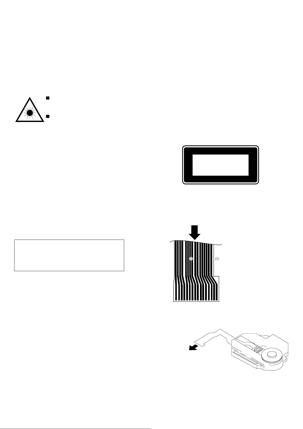
PROTECTION OF EYES FROM LASER BEAM DURING SERVICING
PICK UP ASSY
: SOLDER
910 15161
This set employs laser. Therefore, be sure to follow carefully the
instructions below when servicing.
WARNING!
WHEN SERVICING, DO NOT APPROACH THE LASER EXIT
WITH THE EYE TOO CLOSELY. IN CASE IT IS NECESSARY TO
CONFIRM LASER BEAM EMISSION. BE SURE TO OBSERVE
FROM A DISTANCE OF MORE THAN 30cm FROM THE
SURFACE OF THE OBJECTIVE LENS ON THE OPTICAL
PICK-UP BLOCK.
Caution: Invisible laser radiation when
open and interlocks defeated avoid exposure to beam.
Advarsel:Usynling laserståling ved åbning,
når sikkerhedsafbrydere er ude af funktion.
Undgå udsættelse for stråling.
VAROITUS!
Laiteen Käyttäminen muulla kuin tässä käyttöohjeessa mainitulla tavalla saattaa altistaa käyt-täjän turvallisuusluokan 1 ylittävälle näkymättömälle lasersäteilylle.
VARNING!
Om apparaten används på annat sätt än vad som specificeras i
denna bruksanvising, kan användaren utsättas för osynling
laserstrålning, som överskrider gränsen för laserklass 1.
CAUTION
Use of controls or adjustments or performance of procedures
other than those specified herein may result in hazardous
radiation exposure.
ATTENTION
L'utilisation de commandes, réglages ou procédures autres que
ceux spécifiés peut entraîner une dangereuse exposition aux
radiations.
ADVARSEL!
Usynlig laserståling ved åbning, når sikkerhedsafbrydereer ude
af funktion. Undgå udsættelse for stråling.
This Compact Disc player is classified as a CLASS 1 LASER
product.
The CLASS 1 LASER PRODUCT label is located on the rear
exterior.
CLASS 1
KLASSE 1
LUOKAN 1
KLASS 1
LASER PRODUCT
LASER PRODUKT
LASER LAITE
LASER APPARAT
Precaution to replace Optical block
(SF-P200)
Body or clothes electrostatic potential could ruin
laser diode in the optical block. Be sure ground
body and workbench, and use care the clothes
do not touch the diode.
1) After the connection, remove solder shown in
the right figure.
–3–
Page 4

ELECTRICAL MAIN PARTS LIST
PART NO.
NO.
IC
87-A21-448-040 C-IC,BH6554FV
8A-HCH-602-010 C-IC,MN101C439-AD<714AHC>
8A-HC4-611-010 C-IC,MN101C439AA<EXCEPT 714AHC>
87-A21-453-040 C-IC,RS-351-38KHZ<716C>
87-A21-446-010 C-IC,MN662782RPT1
87-A21-140-040 C-IC,MSM51V17400D
87-A21-578-040 C-IC,AN8838NSB
87-A21-543-040 IC,NJU7012
87-A21-449-040 C-IC,AN8746SA
87-A21-085-040 C-IC,TA2120FN
87-A21-523-040 C-IC,SM8142BD
87-A20-582-010 IC,GP1F31TJ<714AHC>
TRANSISTOR
87-026-608-080 C-TR,DTC 123 JK
87-A30-075-080 C-TR,2SA1235F
89-211-323-080 C-TR,2SB1132R
89-416-643-080 C-TR,2SD1664R
87-A30-076-080 C-TR,2SC3052F
89-113-695-680 C-TR,2SA1369G/H
87-A30-278-040 C-FET,2SK2980
87-026-350-080 C-TR,DTC114TU
87-A30-237-080 C-TR,UMG5N
87-A30-282-040 C-TR,DTA114TKA
87-026-239-080 TR,DTC114TK (0.2W)
DIODE
87-A40-270-080 C-DIODE,MC2838
87-017-520-080 C-DIODE,SFPB52
87-A40-570-080 C-ZENER,UDZ10B
87-A40-590-040 C-DIODE,HRW0202A
87-017-366-080 C-DIODE,DAN202U<716C>
84-XMC-624-080 C-DIODE,1SS250
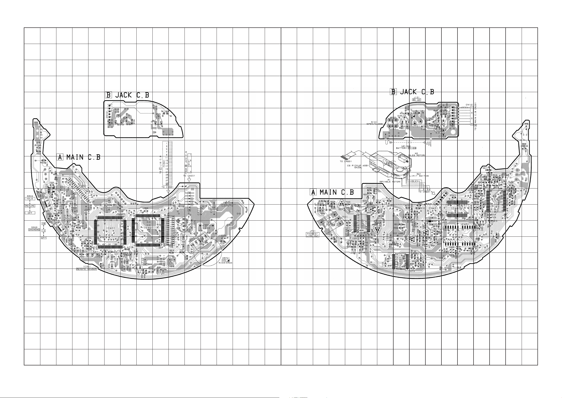
MAIN C.B
C202 87-016-422-080 C-CAP,E 22-6.3
C203 87-012-286-080 CAP, U 0.01-25
C204 87-016-429-080 C-CAP,E 100-4 5.5N
C205 87-010-805-080 C-CAP,S 1-16 Z F
C206 87-012-286-080 C-CAP, U 0.01-25
C207 83-HC3-635-080 C-CAP,E 220-6.3 WF
C208 87-016-426-080 C-CAP,E 47-4 5.5N
C209 87-010-831-080 C-CAP,U,0.1-16F
C210 87-A10-047-080 C-CAP,U 1-10 Z F
C211 87-010-787-080 CAP, U 0.022-25
C212 87-012-267-080 C-CAP,U 270P-50 B
C213 87-010-805-080 C-CAP,S 1-16 Z F
C303 87-010-831-080 C-CAP,U,0.1-16F
C304 87-010-831-080 C-CAP,U,0.1-16F
C305 87-012-286-080 CAP, U 0.01-25
C306 87-012-286-080 CAP, U 0.01-25
C307 87-012-286-080 CAP, U 0.01-25
C309 87-A11-241-080 C-CAP,TN 22-6.3 M F93A
C361 87-A11-241-080 C-CAP,TN 22-6.3 M F93 A<716C>
C362 87-012-286-080 C-CAP, U 0.01-25<716C>
C363 87-012-195-080 C-CAP,U 100P-50<716C>
C383 87-A10-260-080 C-CAP,U 0.1-16 K B<714AHC>
C401 87-016-429-080 C-CAP,E 100-4 5.5N
C403 87-016-558-080 C-CAP,TN 47-6.3 F93 B
C405 87-A10-260-080 C-CAP,U 0.1-16 K B
C406 87-012-271-080 C-CAP,U 560P-50 KB<714AHC>
C406 87-012-273-080 C-CAP,U 820P-50 <EXCEPT 714AHC>
C407 87-010-787-080 CAP, U 0.022-25
C408 87-A10-353-080 C-CAP,U0.22-10KB
C409 87-A10-827-080 C-CAP,U 0.47-6.3 K B
DESCRIPTIONREF. NO. KANRI
PART NO.
NO.
C410 87-012-286-080 CAP, U 0.01-25
C411 87-010-831-080 C-CAP,U,0.1-16F
C412 87-016-558-080 C-CAP,TN 47-6.3 F93 B
C413 87-010-831-080 C-CAP,U,0.1-16F
C414 87-012-188-080 C-CAP,U 47P-50 CH<714AHC>
C415 87-010-831-080 C-CAP,U,0.1-16F
C417 87-012-188-080 C-CAP,U 47P-50 CH
C421 87-010-831-080 C-CAP,U,0.1-16F
C422 87-010-831-080 C-CAP,U,0.1-16F
C423 87-010-831-080 C-CAP,U,0.1-16F
C451 87-010-831-080 C-CAP,U,0.1-16F
C501 87-016-429-080 C-CAP,E 100-4 5.5N
C502 87-010-831-080 C-CAP,U,0.1-16F
C504 87-010-831-080 C-CAP,U,0.1-16F
C505 87-A11-228-080 C-CAP,U 0.027-25 K B
C506 87-012-199-080 CAP 220P
C507 87-012-193-080 C-CAP,U 82P-50 CH
C508 87-012-193-080 C-CAP,U 82P-50 CH
C509 87-012-273-080 C-CAP,U 820P-50 B
C510 87-016-429-080 C-CAP,E 100-4 5.5N
C512 87-016-429-080 C-CAP,E 100-4 5.5N
C514 87-A11-228-080 C-CAP,U 0.027-25 K B
C515 87-A11-228-080 C-CAP,U 0.027-25 K B
C516 87-A10-260-080 C-CAP,U 0.1-16 K B
C518 87-012-176-080 C-CAP,U 15P-50
C519 87-012-176-080 C-CAP,U 15P-50
C520 87-016-426-080 C-CAP,E 47-4 5.5N
C521 87-012-274-080 CHIP CAP,U 1000P-50B
C530 87-A10-047-080 C-CAP,U 1-10 Z F
C601 87-016-430-080 C-CAP,E 100-6.3 5.5N
C602 87-012-286-080 CAP, U 0.01-25
C603 87-012-286-080 C-CAP, U 0.01-25
C701 87-016-558-080 C-CAP,TN47-6.3F93B
C702 87-012-271-080 C-CAP,U 560P-50 CH
C703 87-012-271-080 C-CAP,U 560P-50 CH
C706 87-010-831-080 C-CAP,U 0.1-16F
C707 87-A10-047-080 C-CAP,U 1-10 Z F
C708 87-A10-047-080 C-CAP,U 1-10 Z F
C709 87-A10-047-080 C-CAP,U 1-10 Z F
C710 87-016-561-080 C-CAP,E 10-6.3 MF
C711 87-A11-241-080 C-CAP,TN 22-6.3 M F93 A
C712 87-A10-353-080 C-CAP,U0.22-10KB
C713 87-010-831-080 C-CAP,U,0.1-16F
C714 87-A11-062-080 C-CAP,S 2.2-16 Z F
C715 87-016-561-080 C-CAP,E 10-6.3 MF
C716 87-010-831-080 C-CAP,U,0.1-16F
C717 87-010-831-080 C-CAP,U,0.1-16F
C718 87-016-431-080 C-CAP,E 220-4 5.5N
C719 87-016-431-080 C-CAP,E 220-4 5.5N
C720 87-012-274-080 CHIP CAP,U 1000P-50B
C721 87-012-274-080 CHIP CAP,U 1000P-50B
CN201 87-A61-147-080 C-CONN,7P V ZH-SM3
CN301 87-A60-792-080 C-CONN,30P V 30FLT-SM1TB
CN501 87-009-214-080 C-CONN,16P 52207
CN601 87-009-411-010 CONN,6P ZH V
FC301 8A-HC4-631-010 FF-CABLE, 30P 0.5MM
J701 85-HC5-616-010 JACK,3.5 ST W/R GRN<716C>
J701 87-A60-682-010 JACK,3.5 ST 7P<714>
L201 87-A50-355-080 C-COIL,330UH LQH3C
L202 87-A50-330-080 C-COIL,100UH-D75C
L203 87-A50-355-080 C-COIL,330UH LQH3C
L302 87-A50-367-080 C-COIL, 10UH LQG21F
L401 87-A50-367-080 C-COIL, 10UH LQG21F
L402 87-A50-012-080 C-COIL,100UH LQH3C
L501 87-A50-117-080 C-COIL, 10UH LQH3C
L502 87-A50-367-080 C-COIL, 10UH LQG21F
R361 87-A50-367-080 C-COIL, 10UH LQG21F<716C>
S301 87-A90-493-080 C-SW,SL 1-1-2 SSSS81<714AHC>
S302 87-A90-494-080 C-SW,SL 1-1-3 SSSS81
S303 87-A90-494-080 C-SW,SL 1-1-3 SSSS81
DESCRIPTIONREF. NO. KANRI
–4–
Page 5
PART NO.
NO.
VR701 87-A91-145-080 C-VR,RTRY 30KCX2 H RK14J12R
X401 87-A70-201-080 C-VIB,CER 16.93MHZ CSTCV-MXJ0C
JACK C.B
C102 87-010-060-010 CAP,E 100-16V
C103 87-012-286-080 CAP, U 0.01-25
C104 87-015-677-010 CAP,E 100-6.3V
C105 87-012-286-080 CAP, U 0.01-25
CN101 8A-HC4-633-010 CONN ASSY,7P V 1.5MM
J101 87-A60-421-010 JACK,DC HEC3600 BLK 6
S101 87-A91-622-010 SW,MICRO PV1102
LID C.B
C801 87-016-558-080 C-CAP,TN 47-6.3 F93 B
C802 87-012-274-080 CHIP CAP 1000P
C803 87-010-831-080 C-CAP,U 0.1-16F
C804 87-A10-811-080 C-CAP, 0.1-100 VC30E
D801 87-A91-327-040 C-LED,SEC1703C GRN
D802 87-A91-329-040 C-LED,SECS1803C ORN
D803 87-A91-326-040 C-LED,SEC1603C RED
L801 87-005-843-080 C-COIL,470UH K LQH3C
LCD801 8A-HC4-621-010 LCD,AHC-4 TRANSPAREN
S801 87-A90-232-080 C-SW,TACT SKQRAA
S802 87-A90-232-080 C-SW,TACT SKQRAA
S803 87-A90-232-080 C-SW,TACT SKQRAA
S804 87-A90-232-080 C-SW,TACT SKQRAA
S805 87-A90-232-080 C-SW,TACT SKQRAA
S806 87-A90-232-080 C-SW,TACT SKQRAA
S807 87-A90-232-080 C-SW,TACT SKQRAA
DESCRIPTIONREF. NO. KANRI
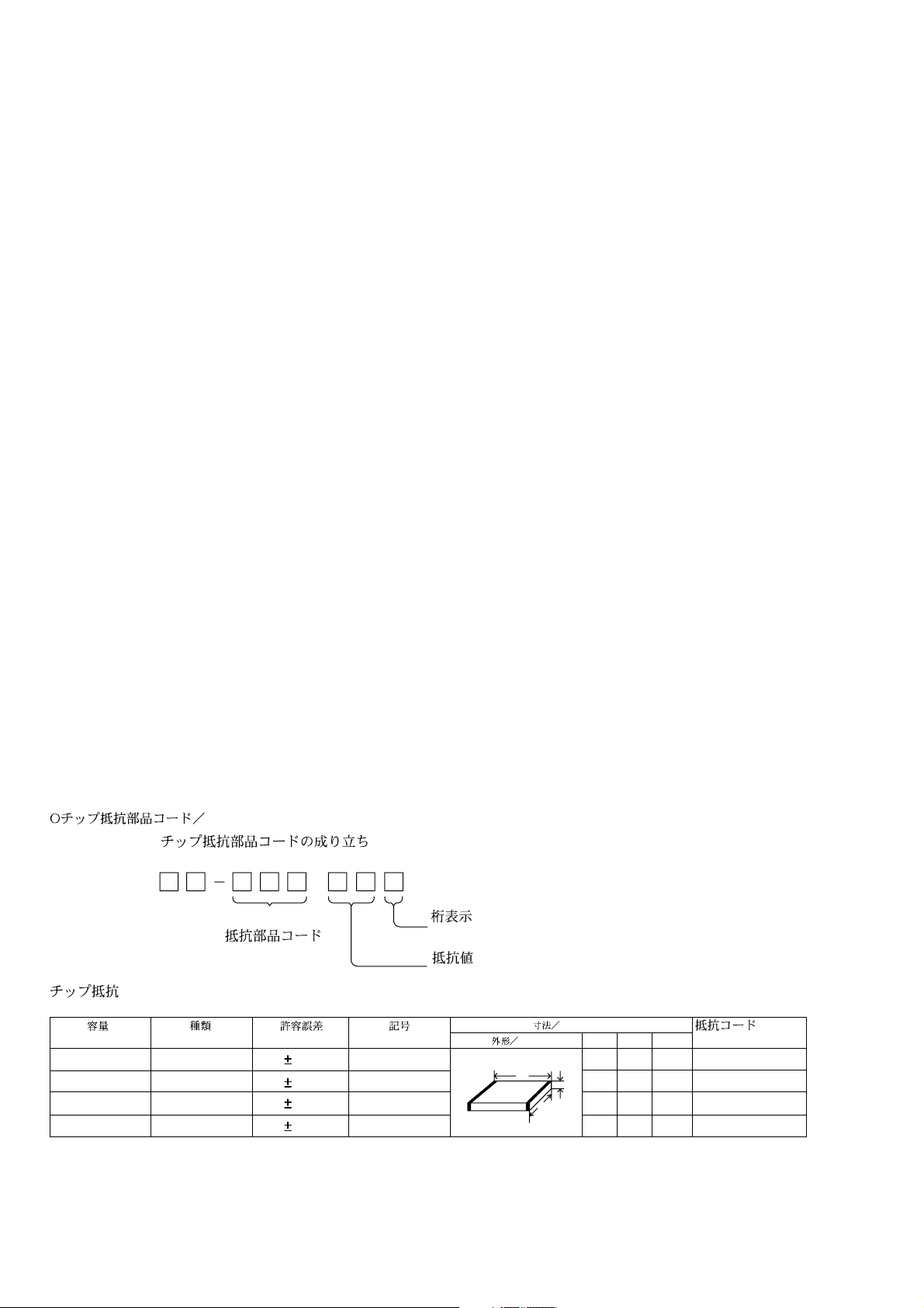
CHIP RESISTOR PART CODE
Chip Resistor Part Coding
88
A
Resistor Code
Chip resistor
Wattage Type Tolerance
1/16W 1005 5% CJ
1/16W
1/10W
1/8W
1608
2125
3216
5%
5%
5%
Symbol
CJ
CJ
CJ
Figure
Value of resistor
Form
L
–5–
Dimensions (mm)
t
W
LW t
1.0 0.5 0.35 104
1.6 0.8 0.45
2 1.25 0.45
3.2
1.6
Resistor Code
0.55
108
118
128
: A
: A
Page 6

TRANSISTOR ILLUSTRATION
C
B
E
2SA1235
2SC3052
DTA114TKA
DTC114TK
DTC114TU
DTC123JK
CBE
2SA1369
2SB1132
2SD1664
G
S
2SK2980
C1
B1
C2
E
B2
D
UMG5N
–6–
Page 7
WIRING - 1 (MAIN / JACK) <XP-V716C>
2
A
A
B
B
C
C
D
D
E
E
F
F
G
G
H
H
876543211345678
9 10 11 12 13 14 15 16910111213141516
I
I
J
J
K
K
L
L
M
M
N
N
O
O
P
P
Q
Q
R
S
T
U
–7–
R
S
T
U
Page 8
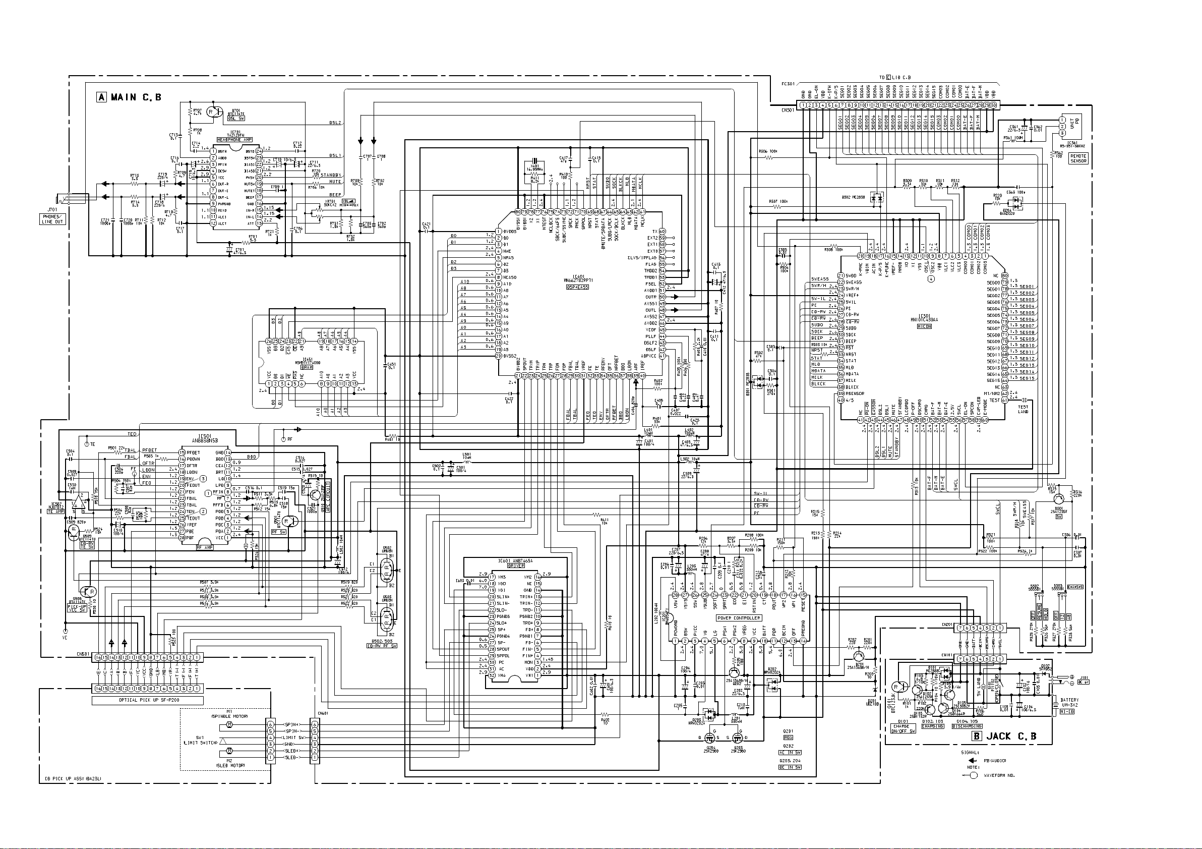
SCHEMATIC DIAGRAM - 1 (MAIN / JACK) <XP-V716C>
–8–
Page 9
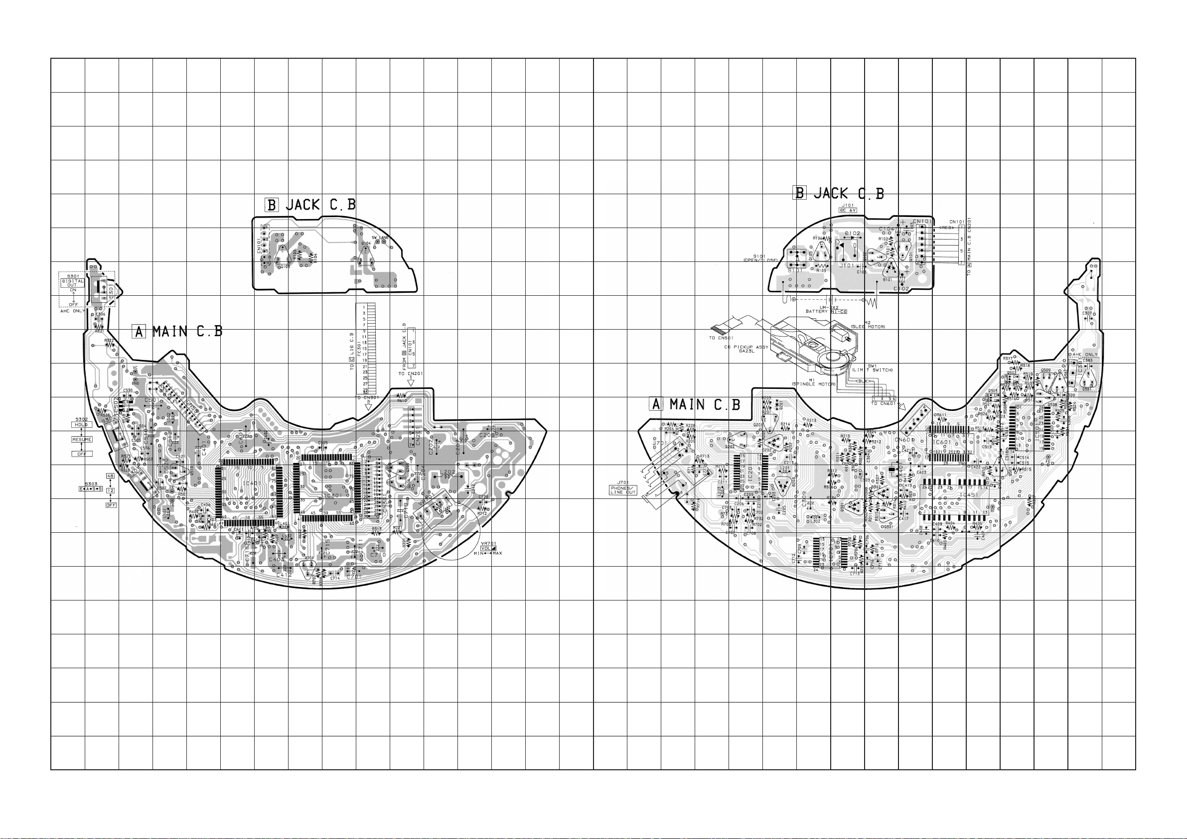
WIRING - 2 (MAIN / JACK) <XP-V714>
2
A
A
B
B
C
C
D
D
E
E
F
F
G
G
H
H
876543211345678
9 10 11 12 13 14 15 16910111213141516
I
I
J
J
K
K
L
L
M
M
N
N
O
O
P
P
Q
Q
R
S
T
U
–9–
R
S
T
U
Page 10

SCHEMATIC DIAGRAM - 2 (MAIN / JACK) <XP-V714>
–10–
Page 11

WIRING - 3 (LID)
101112131415161718192021222324
1234567892526272829303132
A
B
C
D
E
F
G
H
I
J
K
L
M
N
O
P
Q
–11–
R
S
T
U
Page 12

SCHEMATIC DIAGRAM - 3 (LID)
–12–
Page 13

LCD DISPLAY
–13–
Page 14

IC BLOCK DIAGRAM
IC,SM8142BD
IC,AN8746SA
IC,TA2120FN
–14–
Page 15

IC,BH6554FV
IC,AN8838NSB
–15–
Page 16

WAVEFORM
1
IC501 PIN 7 (RF)
IC501 PIN 20 (FEOUT)
3
IC501 PIN 25 (TEOUT)
2
0.5 V/div
0.2 µs/div
50 mV/div
1 ms/div
IC301 PIN 10 (OSC1)
4
50 mV/div
1 ms/div
1 V/div
50 ns/div
–16–
Page 17

IC DESCRIPTION
IC, MN101C439AA / IC, MN101C439-AD
Pin No. Pin Name I/O Description
1 COM03 O LCD common output.
2 COM02 O LCD common output.
3 COM01 O LCD common output.
4 COM00 O LCD common output.
5 VLC3 - LCD drive voltage setting terminal.
6 VLC2 - LCD drive voltage setting terminal.
7 VLC1 - LCD drive voltage setting terminal.
8 VDD - LCD power.
9
10 OSC1 O Micon main clock oscillator output.
11 VSS - GND.
12 XI I Sub clock oscillator (connected to GND).
13 XO O Sub clock oscillator (not used).
14 MMOD I Processor mode unused (connected to GND).
15 VREF- - Connected to GND.
OSC2 O
Micon main clock oscillator output (not used).
16 K-FUNC I "FUNCTION" key input.
17 K-P/S I "PLAY" and "STOP" key inputs.
18 ACIN I AC adaptor detection.
19 VDIN I Main clock (8 MHz).
20 K-RMC I Wired remote control input.
21 SWDO I Digital out "ON/OFF" input. ON at "L" (connected to GND).
22 SWEASS I EASS mode selection input. Refer to A/D table.
23 SWR/H I RESUME/HOLD switch input.
24 VREF+ - Connected to VDD.
25 SWIL I Limited SW input.
26 PC O Power off output for CD serve driver. Power off at "L".
27 CD-RW O CD-RW PLAY gain level selection output. Gain set at "H".
28 CD-RW O CD-RW PLAY gain level selection output. Gain set at "L".
29 SUBQ O Power down output for H/A.
30 SQCK O Selection output for EASS gain control. EASS at "L".
31 BEEP O Buzzer output for headphone.
32 RST I Micro computer RESET input.
33 NRST O DSP RESET output.
34 STAT I DSP STAT input.
35 MLD O DSP MLD output.
36 MDATA O DSP MDATA output.
37 MCLK O DSP MCLK output.
38 BLKCK I DSP BLKCK input.
39 RSENSOR I Wireless remote control sensor signal input.
40 4/5 I XP-V7xx or XP-V5xx selection input. XP-V7xx at "H", XP-V5xx at "L" (not used).
41 NC - Not connected.
42 PU-ON O H/A power down output.
–17–
Page 18

Pin No. Pin Name I/O Description
43 EASSON O EASS gain up selection output. EASS ON at = "L".
44 DSL2 O Headphone DSL2 control output. DSL2 at "H". DSL1/OFF at "L".
45 DSL1 O Headphone DSL ON control output. DSL ON at "H".
46 MUTE O Audio mute output.
47 STANDBY O Headphone standby output. Standby at "L". Power ON at "H".
48 LCDRDO O Wired LCD remote control output.
49 P-OFF O Power IC power off output. Power OFF at "L".
50 DSCHRG O Discharge output.
51 CHRG O Charge output.
52 BAT-F O Battery balance indication FULL INDICATION LED output. LED ON at "L".
53 BAT-M O Battery balance indication MEDIUM INDICATION LED output. LED ON at "L".
54 BAT-E O Battery balance indication EMPTY INDICATION LED output. LED ON at "L".
55 2.5V - Not used.
56 SWCL I Cover OPEN/CLOSE detection switch input .
57 EL-ON O EL back light control output.
58 SPCON O Spindle PWM control output (not used).
59 CAR-LED O CAR-KIT model button LED light output (not used).
60 E-MODE I Shaft damage mode (No shaft damage mode found at "H") (not used).
61 TEST I Enter test mode at "L" (not used).
62 M1/NM2 I 10 or 10/40 sec selection input for XP-V5xx. 10 sec at "H", 10/40 sec at "L". (not used)
63 NC - Not connected.
64 SEG15 O LCD segment output.
65 SEG14 O LCD segment output.
66 SEG13 O LCD segment output.
67 SEG12 O LCD segment output.
68 SEG11 O LCD segment output.
69 SEG10 O LCD segment output.
70 SEG09 O LCD segment output.
71 SEG08 O LCD segment output.
72 SEG07 O LCD segment output.
73 SEG06 O LCD segment output.
74 SEG05 O LCD segment output.
75 SEG04 O LCD segment output.
76 SEG03 O LCD segment output.
77 SEG02 O LCD segment output.
78 SEG01 O LCD segment output.
79 SEG00 O LCD segment output (not used).
80 NC - Not connected.
–18–
Page 19

BATTERY INDICATION
GREEN
C8H D7H
ORANGE
A9H
RED RED
8BH
Lo-Batt
GREEN
ORANGE
B9H
A/D TABLE
HEX K-FUNC (PIN 16) SWEASS (PIN 22) SWR/H (PIN 23) K-P/S (PIN 17)
E8 ~ FF OFF EASS 10 RESUME OFF
CB ~ E8 NOT USED OFF OFF PLAY
AD ~ CA DSL OFF OFF PLAY
90 ~ AC MODE OFF OFF PLAY
71 ~ 8F ENTER EASS 40 HOLD/RESUME PLAY
53 ~ 70 B.S EASS 40 HOLD/RESUME STOP
35 ~ 52 F.S EASS 40 HOLD/RESUME STOP
17 ~ 34 NOT USED OFF OFF STOP
1 ~ 16 OFF OFF OFF OFF
A/D TABLE
HEX K-RMC (PIN 20)
E8 ~ FF OFF
BB ~ E8 NOT USED
89 ~ BA DSL
5F ~ 88 PLAY
42 ~ 5E MODE
2E ~ 41 STOP
1F ~ 2D B.S
OB ~ 1E F.S
00 ~ 0A OFF
–19–
Page 20

IC, MN662782RPT1
Pin No. Pin Name
1 DVDD3 - Power supply for DRAM interface.
2 D0 I/O Input/Output data 0 for DRAM.
3 D1 I/O Input/Output data 1 for DRAM.
4 NWE O Output write enable signal for DRAM.
5 NRAS O Output RAS control signal for DRAM.
6 D2 I/O Input/Output data 2 for DRAM.
7 D3 I/O Input/Output data 3 for DRAM.
8 NCAS0 O Output CAS control signal 0 for DRAM.
9 A10 O Output address signal 10.
10 ~ 14 A8 ~ A4 O Output address signal 8 ~ 4.
15 A9 O Output address signal 9.
16 ~ 19 A0 ~ A3 O Output address signal 0 ~ 3.
20 DVSS2 - Ground for digital circuit.
21 DVDD2 - Power supply for digital circuit.
22 SPOUT O PWM output of spindle.
23 TRVM O PWM output of negative traverse signal.
24 TRVP O PWM output of positive traverse signal.
25 TRM O PWM output of negative tracking signal.
I/O
Description
26 TRP O PWM output of positive tracking signal.
27 FOM O PWM output of negative focus signal.
28 FOP O PWM output of positive focus signal.
29 FBAL O Output for focus balance adjustment.
30 TBAL O Output for tracking balance adjustment.
31 VREF - Reference voltage for DA output (TRVP, TRP, FOM, FOP, FBAL, TBAL, DSLF2).
32 FE I Focus error signal input (analog input).
33 TE I Tracking error signal input (analog input).
34 RFENV I RF envelope signal input (analog input).
35 OFT I Off track signal input. "H" : Off track.
36 NRFDET I RF detection signal input. "L" : Detect.
37 BDO I Drop out signal input. "H" : Drop out.
38 LDON O Laser ON signal output. "H" : ON.
39 ARF I RF signal input.
40 IREF I Reference current input terminal.
41 ADPVCC - Reference voltage level for PWM output drive.
42 DSLF O Loop filter terminal for DSL.
43 DSLF2 O DSL unbalance current.
44 PLLF O Loop filter terminal for PLL.
45 VCOF O Loop filter terminal for pitch controller and jitter free VCO.
46 AVDD2 - Power supply for analog circuit (DSL, PLL, VCOF, AD, DA).
47 AVSS2 - Ground for analog circuit (DSL, PLL, VCOF, AD, DA).
48 OUTL O Output Lch audio.
49 AVSS1 - Ground for analog circuit (for audio output).
–20–
Page 21

Pin No. Pin Name
50 OUTR O Output Rch audio.
51 AVDD1 - Power supply for analog circuit (for audio output).
52 FSEL I Input noise filter ON / OFF switching. "L" : ON. "H" : OFF.
53 TMOD1 I Terminal mode switching input 1 (connected to GND).
54 TMOD2 I Terminal mode switching input 2 (connected to GND).
55 FLAG O Flag signal output (not used).
56 CLVS/IPFLAG - Not used.
57 ~ 59 EXT 0 ~ 2 I/O Expansion input / output port 0 ~ 2 (not used).
60 TX O Digital audio interface output signal.
61 MCLK I Microcomputer command clock signal input (latch data at rising edge).
62 MDATA I Microcomputer command data signal input.
63 MLD I Microcomputer command load signal input. "L" : Load.
I/O
Description
64 BLKCK I
65 SQCK/BCLK I Input clock for sub code Q register.
66 SUBQ/LRCK O Output sub code Q data.
67 DMUTE/SRDATA I Input mute. "H" : Mute (connected to GND).
68 STAT O
69 NRST I Input reset. "L" : Reset.
70 SPPOL O PWM output of spindle signal drive.
71 PMCK O 88.2kHz clock signal output (not used).
72 SMCK O 4.2336MHz clock signal output.
73 SUBC/SSYNC O Output sub code serial (not used).
74 SBCK/64FS I Input clock for subcode serial (not used).
75 NCLDCK O Sub code frame clock signal output ( fCLDCK = 7.35kHz). (Not used)
76 NTEST - Test terminal (connected to power supply).
77 X1 I Crystal oscillator circuit input terminal (f = 16.93MHz).
78 X2 O Crystal oscillator circuit output terminal (f = 16.93MHz).
79 DVDD1 - Power supply for digital circuit.
Input sub code block clock signal (fBLKCK = 75kHz) / Input SYNC signal for
CDTEXT (fDQSY = 300kHz).
Output status signal (CRC,RESY,CLVS,NTTSTOP,SQOK,FLAG6,SENSE,NFLOCK,
NTLOCK,BSSEL,SUBQDATA,CDTEXT DATA,ANT-SHOCK READ OUT DATA.)
80 DVSS1 - Ground for digital circuit.
–21–
Page 22

TEST MODE
A MAIN C.B
VC
GND
CN201
A MAIN C.B
FE
TE
IC401
IC301
CN301
VR701
IC501
B JACK C.B
J101
CN101
IC201
SW
LAND
S101
TEST LAND
IC701
–22–
CN601
IC601
IC451
FE
RF
Page 23

The servo circuit of this model is designed to be adjustment-free and the adjustment value and disc distinction (CA-DA. CD-R and CDRW etc.) is adjusted by within the IC. Therefore the adjustment is performed by each TOC reading. The adjustment conditions within the
IC of each servo can be monitored in this test mode.
1. How to start the Test Mode
Starting method of the test mode differ depending upon the type of disc being used. This is because the adjustment values of each
servo also differ depending upon the type of disc.
When using the CD-DA or CD-R
1) Short-circuit the test land and the OPEN/CLOSE SW land.
2) Insert the AC plug and install the CD-DA or CD-R disc.
3) Press the PLAY and STOP buttons in this sequence and read the TOC.
4) Press the DISPLAY/ENTER button and confirm that all LCD light up.
When using the CD-RW
1) Short-circuit the test land and the OPEN/CLOSE SW land.
2) Insert the AC plug and install the CD-RW disc.
3) Press the PLAY, STOP and DSL buttons in this sequence and read the TOC. The LCD display should display CD-r at this point.
4) Press the DISPLAY/ENTER button and confirm that all LCD light up.
Note 1) If the TOC cannot be read, press the DISPLAY/ENTER button once “Err” has appeared on the LCD, causing all the LCDs to
become lit up. The following steps 2 and 3 can be confirmed even if the TOC cannot be read.
Note 2) By repeatedly pressing the DISPLAY/ENTER button, all LCD will light up and the TOC display will be repeated.
Note 3) By repeatedly pressing the DSL button, the “CD-d” and “CD-r” displays will be repeated.
When the LCD displays “CD-d,” → CD-DA, CD-R is selected.
When the LCD displays “CD-r,” → CD-RW is selected.
Note 4) The test mode is cancelled by disconnecting the AC plug and removing the soldering of short land.
2. DISC distinction (confirmation of FE waveform)
This mode is possible to perform a confirmation of the disc distinction.
Confirmation method
1) Press the DSL button and select “CD-d” or “CD-r” (Refer to Note 3).
2) Install the disc.
3) Press the MODE button.
The LCD will change as follows.
Example: Test disc: TCD-782, DISC type select: CD-d, Judgement value: 7F, Measurement value: 3D BE.
Judgement value Measurement value
*All numerical values are displayed in HEX
What disc the IC has selected can be understood according to this judgment value.
The decision standard of IC is as follow.
LCD displays “CD-r”
LCD displays “CD-d”
0 < Judgment value < 10 No disc No disc
10 < Judgment value < 32 CD-RW No disc
32 < Judgment value < C8 CD-DA and CD-R CD-RW
C8 < Judgment value CD-DA and CD-R
The state of the FE waveform can also be understood from this judgment value.
3. Confirmation of sled movement
By pressing the F. SKIP or B. SKIP button continuously when all LCD light up, it is possible to transfer the pick-up to either the outer
circumference or the inner circumference (the LCD is to remain all light up).
–23–
Page 24

4. Confirmation of the RF level
Test point: RF and VC (Vref)
Test disc: TCD-782
Confirm that the RF waveform appears as shown below.
VOLT/DIV: 200mV
TIME/DIV: 0.5us
At 0.8 Vp-p or greater
5. Confirmation of tracking balance
Test point: TE and VC (Vref)
Test disc: TCD-782
Press the DSL button while the test disc is playing and confirm that the traverse waveform is as is shown below.
VC
VOLT/DIV: 200mv
TIME/DIV: 2ms
6. Confirmation of each servo
It is possible to confirm the adjustment value of each servo by repeatedly pressing the MODE button while the test disc is playing. The
switchover sequence is as stated below.
Confirmation mode OFF -> Focus bias (FB) -> Tracking balance (TB) -> Tracking gain (TG) -> Tracking error offset (TEO) -> Focus
gain (FG) -> Focus error offset (FEO) -> Confirmation mode OFF
Example: Tracking error offset (TEO) Adjustment value-> 03
Tracking error offset (TEO) display Adjustment value
*Adjustment values are displayed in HEX.
–24–
Page 25

MECHANICAL EXPLODED VIEW 1 / 1
–25–
Page 26

MECHANICAL EXPLODED PARTS LIST 1 / 1
PART NO.
NO.
1 8A-HC4-010-010 SH,DISPLAY (4)<[S]716C>
1 8A-HC4-028-010 SH,DISPLAY EZ(V714)<EXCEPT [S]716C>
2 8A-HC4-016-210 PANEL,CD (4)
3 8A-HC4-007-110 PANEL,LED
4 8A-HC4-005-010 LENS,LED
5 8A-HC4-006-110 KEY,PLAY (4)
6 8A-HC4-001-110 LID,CD (4)<[S]716C,[S]714AHC>
6 8A-HC4-020-010 LID,CD GOLD(4)<[N]714AK,[N]714AEZ>
7 8A-HC4-208-010 PLATE,LCD
8 8Z-HC4-201-010 JOINT,LCD ZHC-4
9 8A-HC4-011-010 HLDR,LID CD (4)
10 8A-HC4-204-110 SPR-T,LID
11 85-HC6-205-110 SHAFT,LID(300) HK
12 8A-HC4-002-110 CABI,CENTER (4)<[S]716C>
12 8A-HC4-044-010 CABI,CENTER GOLD(V714)<[N]714AK,[N]714AEZ>
12 8A-HC4-030-010 CABI,CENTER HR(V714)<[S]714AHC>
13 8A-HC4-008-110 KNOB,SL OPEN
14 8A-HC4-014-010 WINDOW,SENSOR<[S]716C>
15 8A-HC4-205-010 SPR-T,KNOB
16 8A-HC4-206-110 LEVER,OPEN
17 8A-HC4-207-010 HLDR,OPEN
18 8Z-HC1-225-010 DMPR,MECHA(SP)
19 8A-HC4-202-010 BAT-CONTACT,(+)
20 8A-HC4-201-110 BAT-CONTACT,(-)
21 8A-HC4-203-110 BAT-CONTACT,(+-)
22 8A-HC4-013-110 CABI,BOTTOM ASSY (4)<[S]716C>
22 8A-HC4-027-010 CABI,BOTTOM ASSY EZ (V714)<[N]714AK,[N]714AEZ>
22 8A-HC4-032-110 CABI,BOTTOM ASSY HR (V714)<[S]714AHC>
23 88-HC6-021-010 FOOT, DIA10
24 8A-HC4-009-010 KNOB,SL HOLD
25 87-HC4-014-010 COVER, OPT<[S]714AHC>
26 8A-HM1-599-010 W,1.7-3.6-0.23 W/ADH
A 87-067-736-010 SCREW,1.4-2 BLK NLOCK
B 87-067-732-010 TAPPING SCREW, VT1.4-3
C 87-067-869-010 V+1.7-8 HL BLK
DESCRIPTIONREF. NO. KANRI
COLOR NAME TABLE
Basic color symbol Color Basic color symbol Color Basic color symbol Color
B Black C Cream D Orange
G Green H Gray L Blue
LT Transparent Blue N Gold P Pink
R Red S Silver ST Titan Silver
T Brown V Violet W White
WT Transparent White Y Yellow YT Transparent Yellow
LM Metallic Blue LL Light Blue GT Transparent Green
LD Dark Blue DT Transparent Orange GM Metallic Green
YM Metallic Yellow DM Metallic Orange
–26–
Page 27

CD MECHANISM EXPLODED VIEW 1 / 1
D
D
2
4
9
A
3
5
1
7
8
C
6
10
B
–27–
Page 28

CD MECHANISM PARTS LIST 1 / 1
PART NO.
NO.
1 S0-A41-A20-600 PICKUP LASER ASSY
2 SM-10A-108-001 MOTOR ASSY SPINDLE
3 S0-M10-A10-900 MOTOR SLED ASSY
4 S2-311-A12-200 CHASSIS
5 S2-511-A23-200 GEAR MIDDLE
6 S2-511-A23-100 GEAR,SCREW
7 S2-511-A23-400 GEAR,RACK
8 S2-511-A07-900 SPINDLE SCREW
9 S4-S13-A00-200 SW,LEAF
10 S2-451-A18-100 HOLDER GEAR
A SS-EXE-A04-000 SCR PAN PCS 1.4-2.2
B SS-GXE-A00-300 SPECIAL SCREW
C SS-EXE-A14-100 SPECIAL SCREW
D SS-GXE-A00-202 SPECIAL SCREW M1.7-4.0
DESCRIPTIONREF. NO. KANRI
ACCESSORIES / PACKAGE LIST
PART NO.
1 8A-HC4-902-110 IB,HC (ECC) - IN <714AHC>
1 8A-HC4-904-010 IB,EZ (EGF) - IN <714AEZ,714AK>
1 8A-HC4-916-010 IB,Y (EGF) - IN <716CY>
2 87-B30-283-010 AC ADAPTOR,AC-D603ENC <714AEZ>
!
2 87-B30-284-010 AC ADAPTOR,AC-D603KNC <714AK>
!
2 87-B30-286-010 AC ADAPTOR,AC-D603HCNC <714AHC>
!
3 87-B30-328-010 HEADPHONE,HP-M050 <714AK,714AEZ,714AHC>
3 87-B30-265-010 HEADPHONE,HP-M043 <716CY>
4 8A-HC4-101-010 RC UNIT,RC-V716C <716CY>
4 8Z-HC4-100-010 RC UNIT,RC-V714 <714AK,714AEZ,714AHC>
5 86-YK1-001-210 ADAPTOR,CAP-6 <716CY>
6 86-YK1-002-010 ADAPTOR,DC-602 <716CY>
NO.
DESCRIPTIONREF. NO. KANRI
–28–
Page 29

2–11, IKENOHATA 1–CHOME, TAITO-KU, TOKYO 110, JAPAN TEL:03 (3827) 3111
Printed in Singapore9920588 9630472 0251431
 Loading...