

Aiwa XP-V412 AEZ1B, XP-V412 AK1, XP-V412 AEZ1, XP-V411 AHRJ1, XP-V411 AEZ1 Service Manual
...Page 1
XP-V410
XP-V411
XP-V412
Y1(S) YJ1(LT)
AEZ1(L) AHRJ1(S)
AEZ1(S) AHRJ1(LT)
AK1(S) AEZ1B(G)
AEZ1(S) AEZ1B(S)
SERVICE MANUAL
COMPACT DISC PLAYER
This Service Manual is the "Revision Publishing" and replaces "Simple Manual"
(S/M Code No. 09-003-342-6T1).
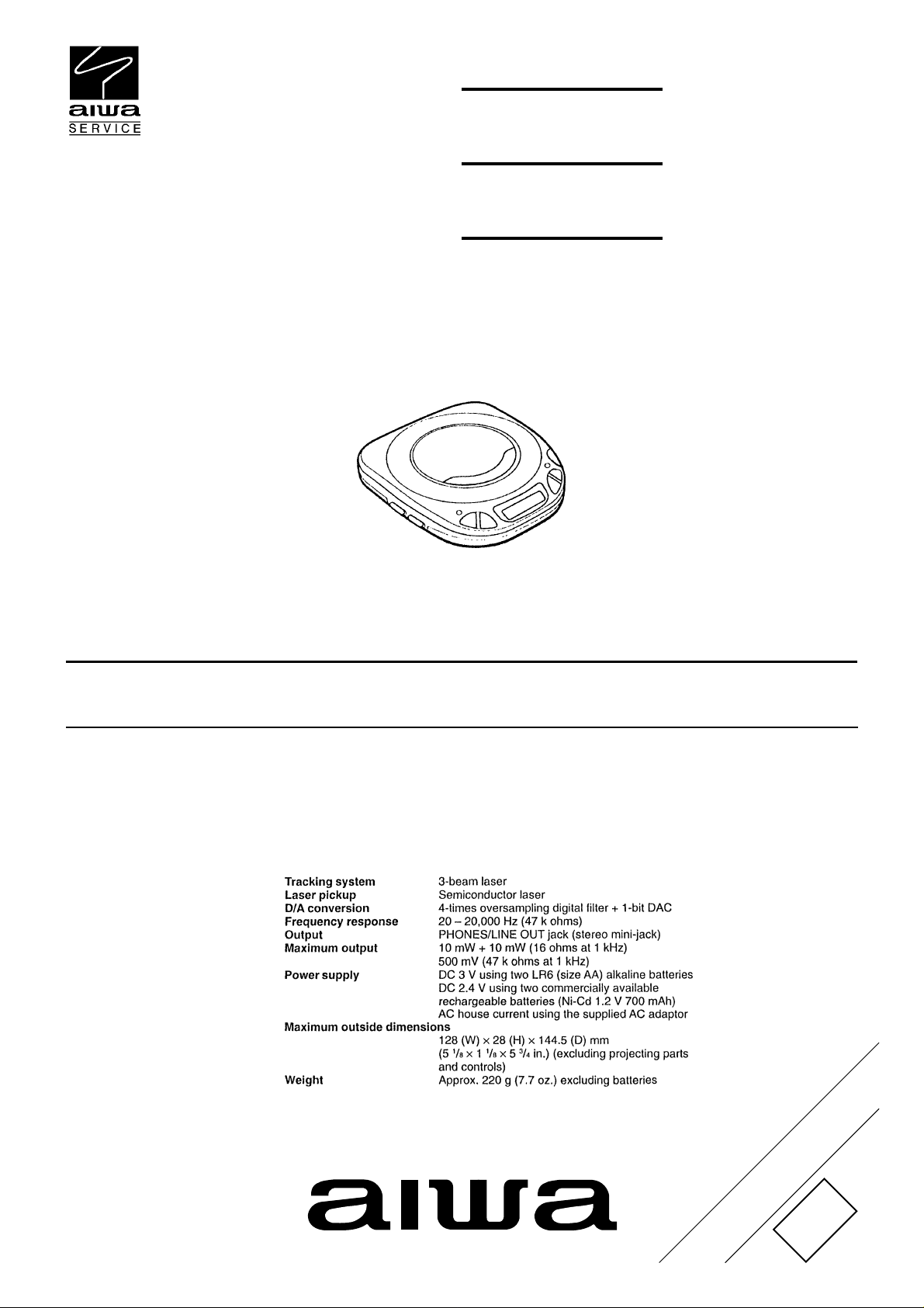
SPECIFICATIONS
BASIC CD MECHANISM : DA23L
Design and specifications are subject to change without
•
.
notice
S/M Code No. 09-003-342-6R1
REVISION
DATA
Page 2
PROTECTION OF EYES FROM LASER BEAM DURING SERVICING
This set employs laser. Therefore, be sure to follow carefully the
instructions below when servicing.
WARNING!
WHEN SERVICING, DO NOT APPROACH THE LASER EXIT
WITH THE EYE TOO CLOSELY. IN CASE IT IS NECESSARY TO
CONFIRM LASER BEAM EMISSION. BE SURE TO OBSERVE
FROM A DISTANCE OF MORE THAN 30cm FROM THE
SURFACE OF THE OBJECTIVE LENS ON THE OPTICAL
PICK-UP BLOCK.
Caution: Invisible laser radiation when
open and interlocks defeated avoid exposure to beam.
Advarsel:Usynling laserståling ved åbning,
når sikkerhedsafbrydere er ude af funktion.
Undgå udsættelse for stråling.
VAROITUS!
Laiteen Käyttäminen muulla kuin tässä käyttöohjeessa mainitulla tavalla saattaa altistaa käyt-täjän turvallisuusluokan 1 ylittävälle näkymättömälle lasersäteilylle.
VARNING!
Om apparaten används på annat sätt än vad som specificeras i
denna bruksanvising, kan användaren utsättas för osynling
laserstrålning, som överskrider gränsen för laserklass 1.
CAUTION
Use of controls or adjustments or performance of procedures
other than those specified herein may result in hazardous
radiation exposure.
ATTENTION
L'utilisation de commandes, réglages ou procédures autres que
ceux spécifiés peut entraîner une dangereuse exposition aux
radiations.
ADVARSEL!
Usynlig laserståling ved åbning, når sikkerhedsafbrydereer ude
af funktion. Undgå udsættelse for stråling.
This Compact Disc player is classified as a CLASS 1 LASER
product.
The CLASS 1 LASER PRODUCT label is located on the rear
exterior.
CLASS 1
KLASSE 1
LUOKAN 1
KLASS 1
LASER PRODUCT
LASER PRODUKT
LASER LAITE
LASER APPARAT
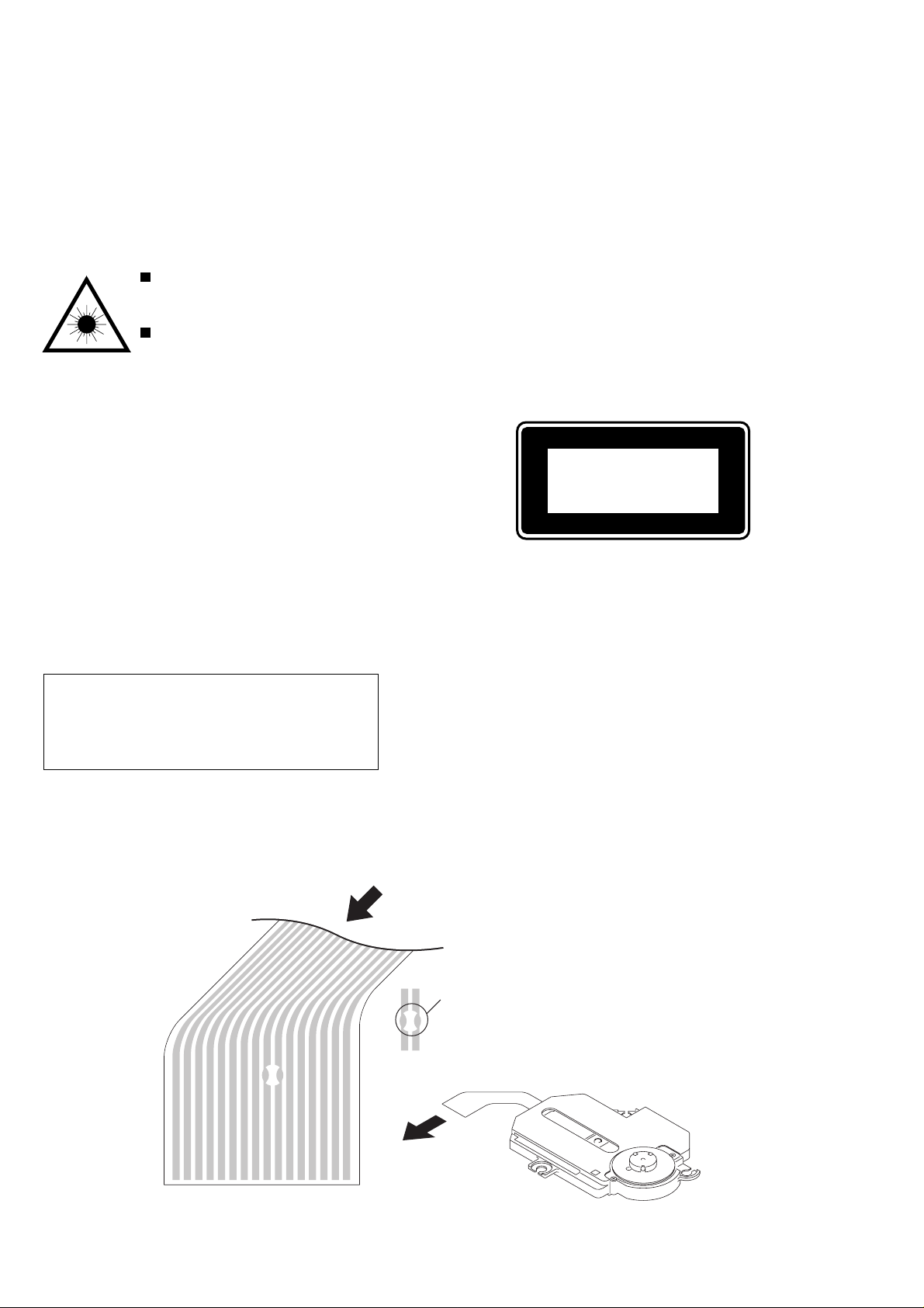
Precaution to replace Optical block
(SF-P200)
Body or clothes electrostatic potential could ruin
laser diode in the optical block. Be sure ground
body and workbench, and use care the clothes
do not touch the diode.
1) After the connection, remove solder shown in
the right figure.
:SOLDER
10 9
PICK UP ASSY
116
SF-P200
2
Page 3

ELECTRICAL MAIN PARTS LIST
REF. NO PART NO. KANRI DESCRIPTION
IC
87-A21-082-040 C-IC,BA6655AFV
8A-HCH-602-010 C-IC,MN101C439-XXX
87-A21-446-010 C-IC,MN662782RPT1
87-A21-568-040 C-IC,GLT441M04
87-A21-578-040 C-IC,AN8838NSB
87-A21-543-040 C-IC,NJU7012
87-A21-521-040 C-IC,BH6517FS
87-A21-085-040 C-IC,TA2120FN
TRANSISTOR
89-211-323-080 C-TR,2SB1132R
87-A30-332-040 C-TR,CPH3106
87-A30-333-040 C-TR,CPH3206
87-026-608-080 C-TR,DTC 123 JK
89-111-625-080 TR,2SA1162 (0.15W)
89-416-643-080 C-TR,2SD1664R
89-327-125-080 CHIP TR,2SC2712GR
87-026-680-080 C-TR,IMH4A
87-026-268-080 C-TR,RN2411
87-026-239-080 TR,DTC114TK (0.2W)
89-324-121-080 C-TR,2SC2412K
87-026-235-080 CHIP-TR,DTC114EK
DIODE
87-A40-614-040 C-DIODE,SFPB-72
87-020-591-080 C-ZENER,02CZ 11Y
87-A40-554-040 C-DIODE,RB491D
87-A40-469-040 C-DIODE,HSM2838CTR
87-020-331-080 CHIP-DIODE,DAN202K
87-002-882-080 C-DIODE,RB425D
MAIN C.B
C101 87-010-060-040 CAP,E 100-16
C102 87-010-197-080 CAP, CHIP 0.01 DM
C103 87-010-197-080 CAP, CHIP 0.01 DM
C105 87-012-156-080 C-CAP,S 220P-50 CH
C106 87-010-483-040 CAP,E 220-4 7L SRA
C107 87-010-194-080 CAP, CHIP 0.047
C108 87-010-178-080 CHIP CAP 1000P
C109 87-A12-158-040 CAP,E 100-4 M 7L SRA
C110 87-012-141-080 CHIP-CAPACITOR,0.22-16F
C111 87-A10-505-080 CAP,E 220-6.3 SF
C112 87-010-805-080 CAP, S 1-16
C113 87-010-196-080 CHIP CAPACITOR,0.1-25
C301 87-A10-488-040 CAP,E 47-4 7L SR
C302 87-010-197-080 CAP, CHIP 0.01 DM
C303 87-010-196-080 CHIP CAPACITOR,0.1-25
C304 87-010-196-080 CHIP CAPACITOR,0.1-25
C305 87-010-197-080 CAP, CHIP 0.01 DM
C306 87-010-197-080 CAP, CHIP 0.01 DM
C307 87-010-197-080 CAP, CHIP 0.01 DM
C308 87-010-309-080 C-CAP,1000P-50 CH
C309 87-010-196-080 CHIP CAPACITOR,0.1-25
C401 87-016-557-040 CAP,E 100-6.3 SF
C403 87-015-677-040 CAP,E 100-6.3 7L
C406 87-A11-550-080 C-CAP,S 820P-50 K B
C407 87-010-198-080 CAP, CHIP 0.022
C408 87-016-460-080 C-CAP,S 0.22-16 B
C409 87-016-526-080 C-CAP,S 0.47-16 BK
C410 87-010-197-080 CAP, CHIP 0.01 DM
C412 87-A12-158-040 CAP,E 100-4 M 7L SRA
C414 87-010-318-080 C-CAP,S 47P-50 CH
C417 87-010-318-080 C-CAP,S 47P-50 CH
C418 87-010-146-080 CHIP CAP 2PF
C419 87-010-146-080 CHIP CAP 2PF
NO.
REF. NO PART NO. KANRI DESCRIPTION
C451 87-010-196-080 CHIP CAPACITOR,0.1-25
C501 87-A12-158-040 CAP,E 100-4 M 7L SRA
C505 87-012-365-080 C-CAP,S 0.027-25VBK
C506 87-012-156-080 C-CAP,S 220P-50 CH
C507 87-010-321-080 CHIP CAPACITOR,82P(J)
C508 87-010-321-080 CHIP CAPACITOR,82P(J)
C509 87-A11-550-080 C-CAP,S 820P-50 K B
C510 87-A12-158-040 CAP,E 100-4 M 7L SRA
C511 87-010-196-080 CHIP CAPACITOR,0.1-25
C512 87-A10-488-040 CAP,E 47-4 7L SR
C513 87-010-196-080 CHIP CAPACITOR,0.1-25
C514 87-012-365-080 C-CAP,S 0.027-25VBK
C515 87-012-365-080 C-CAP,S 0.027-25VBK
C516 87-010-196-080 CHIP CAPACITOR,0.1-25
C518 87-010-312-080 C-CAP,S 15P-50 CH
C520 87-A10-488-040 CAP,E 47-4 7L SR
C521 87-012-349-080 C-CAP,S 1000P-50 CH
C522 87-010-805-080 CAP, S 1-16
C523 87-010-805-080 CAP, S 1-16
C524 87-010-154-080 CAP CHIP 10P
C601 87-A12-158-040 CAP,E 100-4 M 7L SRA
C602 87-010-197-080 CAP, CHIP 0.01 DM
C603 87-010-805-080 CAP, S 1-16
C604 87-010-197-080 CAP, CHIP 0.01 DM
C605 87-010-196-080 CHIP CAPACITOR,0.1-25
C606 87-010-196-080 CHIP CAPACITOR,0.1-25
C607 87-010-197-080 CAP, CHIP 0.01 DM
C610 87-010-805-080 CAP, S 1-16
C701 87-A12-158-040 CAP,E 100-4 M 7L SRA
C702 87-010-854-080 C-CAP,S 560PCH
C703 87-010-854-080 C-CAP,S 560PCH
C706 87-012-368-080 C-CAP,S 0.1-50 F
C707 87-A10-826-080 C-CAP,S 1-10 K B
C708 87-A10-826-080 C-CAP,S 1-10 K B
C709 87-A10-826-080 C-CAP,S 1-10 K B
C710 87-015-681-040 E/CAP 10-16
C711 87-A10-488-040 CAP,E 47-4 7L SR
C712 87-012-141-080 CHIP-CAPACITOR,0.22-16F
C713 87-012-368-080 C-CAP,S 0.1-50 F
C714 87-015-696-040 CAP,E 2.2-50 SRA
C715 87-015-681-040 E/CAP 10-16
C716 87-012-368-080 C-CAP,S 0.1-50 F
C717 87-012-368-080 C-CAP,S 0.1-50 F
C718 87-010-483-040 CAP,E 220-4 7L SRA
C719 87-010-483-040 CAP,E 220-4 7L SRA
C720 87-010-178-080 CHIP CAP 1000P
C721 87-010-178-080 CHIP CAP 1000P
C722 87-012-368-080 C-CAP,S 0.1-50 F
C723 87-010-197-080 CAP, CHIP 0.01 DM
CN501 87-A61-104-010 CONN,16P H WHITE 52089-1610
CN601 87-009-411-010 CONN,6P ZH V
FB701 83-XM1-617-080 C-COIL,BK2125HM601
FB702 83-XM1-617-080 C-COIL,BK2125HM601
FB703 83-XM1-617-080 C-COIL,BK2125HM601
FB704 83-XM1-617-080 C-COIL,BK2125HM601
J101 87-A60-421-010 JACK,DC HEC3600 BLK 6
J701 85-HC5-616-010 JACK,3.5 ST W/R GRN
L101 87-005-770-080 COIL,47UH 7607
L301 87-A50-367-080 C-COIL, 10UH LQG21F
L401 87-A50-556-080 C-COIL, 47UH K LQH3C
L402 87-A50-440-080 C-COIL, 100UH K LQH3C34
L501 87-A50-367-080 C-COIL, 10UH LQG21F
L502 87-A50-367-080 C-COIL, 10UH LQG21F
L601 87-A50-580-080 COIL,470UH LHL06NB
LCD101 8A-HC7-602-010 LCD,AHC-7
R115 87-022-525-080 C-RES,S 20K-1/10W F
R116 87-022-355-080 C-RES,S10K-1/10W F
S301 87-A90-163-010 SW,SL1-1-2 HSW1060
S302 87-A91-742-010 SW,SL 4-1-3 HSW2061-010010
S303 87-A91-622-010 SW,MICRO PV1102
NO.
3
Page 4
REF. NO PART NO. KANRI DESCRIPTION
S304 87-A90-095-080 SW,TACT EVQ11G04M
S305 87-A90-095-080 SW,TACT EVQ11G04M
S306 87-A90-095-080 SW,TACT EVQ11G04M
S307 87-A90-095-080 SW,TACT EVQ11G04M
S308 87-A90-095-080 SW,TACT EVQ11G04M
S309 87-A90-095-080 SW,TACT EVQ11G04M
VR701 87-A90-462-010 VR,RTRY 30KCX2 H RK14J12A0
X401 87-A70-202-080 C-VIB,CER 16.93MHZ CSACV-MXJ04
NO.
• Regarding connectors, they are not stocked as they are not the initial order items.
The connectors are available after they are supplied from connector manufacturers upon the order is received.
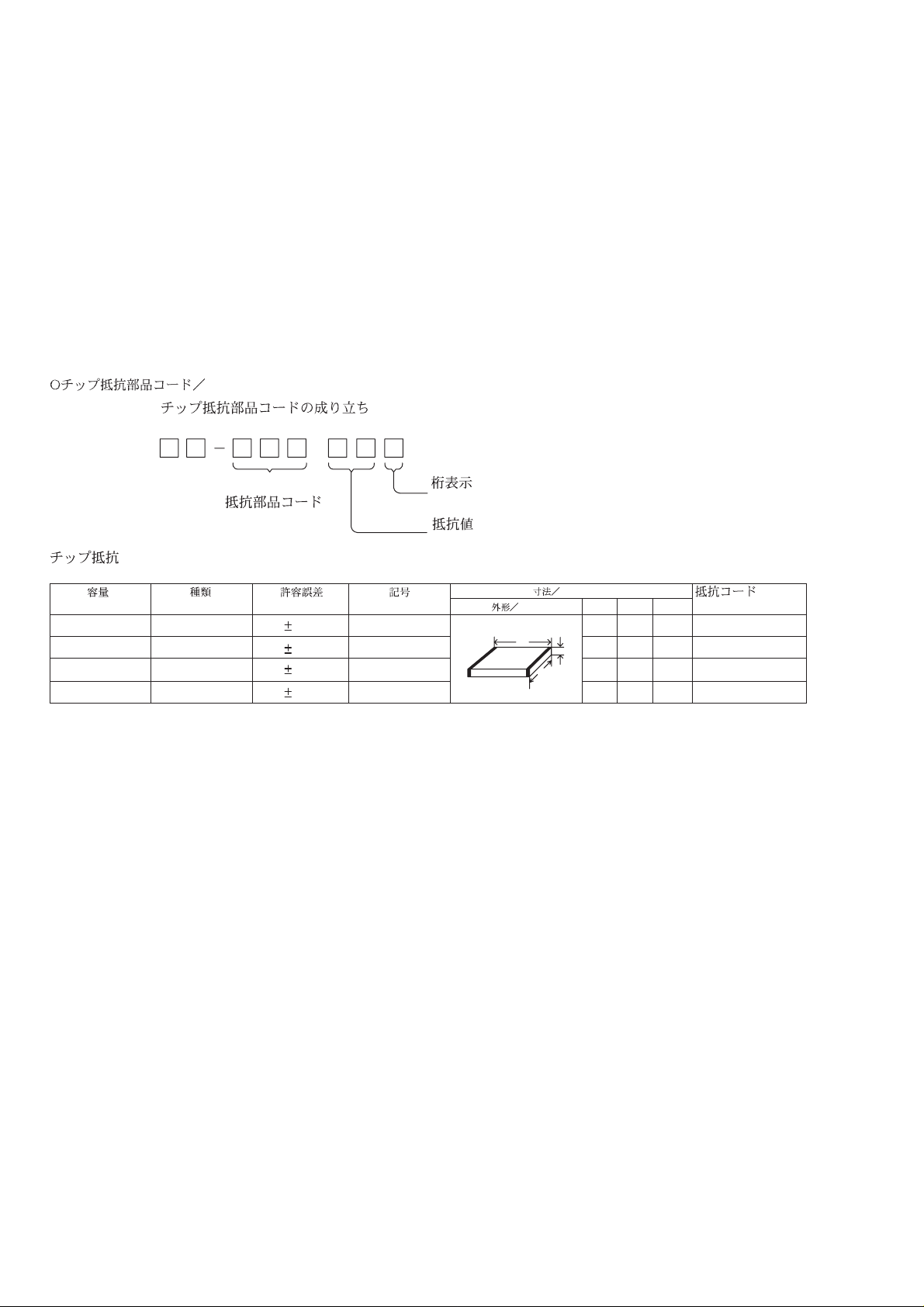
CHIP RESISTOR PART CODE
Chip Resistor Part Coding
88
A
Resistor Code
Chip resistor
Wattage Type Tolerance
1/16W 1005 5% CJ
1/16W
1/10W
1/8W
1608
2125
3216
5%
5%
5%
Symbol
CJ
CJ
CJ
Figure
Value of resistor
Form
L
Dimensions (mm)
t
W
0.55
Resistor Code
108
118
128
LW t
1.0 0.5 0.35 104
1.6 0.8 0.45
2 1.25 0.45
3.2
1.6
: A
: A
4
Page 5

TRANSISTOR ILLUSTRATION
C1
C
B2
E2
B
E
2SA1162
2SC2412
2SC2712
CPH3106
CPH3206
DTC114EK
DTC114TK
DTC123JK
RN2411
E1
B1
C2
BCE
IMH4A 2SB1132
2SD1664
5
Page 6

LCD DISPLAY
LCD, AHC-7
6
Page 7
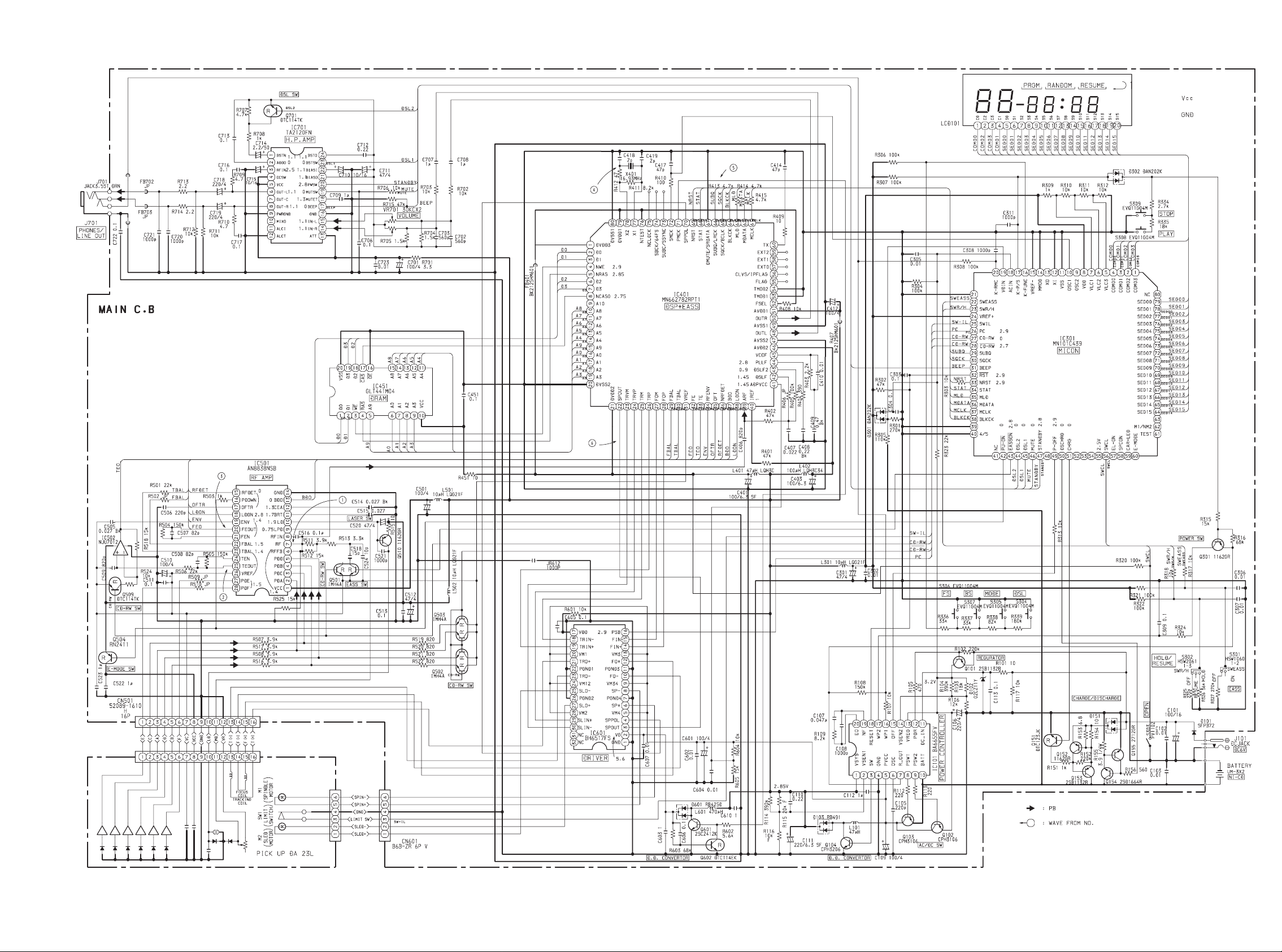
SCHEMATIC DIAGRAM
FB701
BK2125HM601
FB704
BK2125HM601
HSM2838CTR
87
Page 8

WIRING-1 (MAIN :COMPONENT SIDE)
14
13 12 11 10 9 8
7
6
5
432
1
A
B
C
D
E
F
G
H
I
J
109
Page 9

WIRING-2 (MAIN :CONDUCTOR SIDE)
1
A
B
C
D
234567
8
9
10
11 12 13
14
E
F
G
H
I
J
1211
Page 10

TEST MODE
OPEN/CLOSE SW
SHORT LAND
S303
VC
TE
The servo circuit of this model is designed to be adjustment-free and the adjustment value and disc distinction (CD-DA, CD-R and CDRW) etc. is adjusted by the IC. Therefore the adjustment is performed at each TOC reading. The adjustment conditions in the IC of each
servo can be monitored in this test mode.
1. How To Start The Mode
Starting method of the test mode differ depending upon the type of disc being used. This is because the adjustment values of each
servo also differ depending upon the type of disc.
When using the CD-DA or CD-R
1) Short-circuit TEST LAND and OPEN/CLOSE SW land.
2) Insert the AC plug to the power outlet and install the CD-DA or CD-R disc.
3) Press the PLAY and STOP buttons in this sequence and read the TOC.
IC701
IC401
IC451
IC502
20
7
IC601
IC501
RF
FE
When using the CD-RW
1) Short-circuit the TEST LAND and OPEN/CLOSE SW land.
2) Insert the AC plug to the power outlet and install the CD-RW disc.
3) Press the PLAY, STOP and DSL buttons in this sequence and read the TOC. The LCD should display “CD-r” at this point.
Note 1: If the TOC cannot be read, “ERR” has appeared on the LCD. The following step 2 and 3 can be verified even if the “TOC”
cannot be read.
Note 2: By repeatedly pressing the DISPLAY/ENTER button all the LCDs light up and the “TOC” display is repeated.
Note 3: By repeatedly pressing the DSL button the LCD “CD-r” and “CD-d” are repeated.
When the LCD displays “CD-d” ™CD-DA, CD-R is selected.
When the LCD displays “CD-r” ™CD-RW is selected.
Note 4: The test mode is canceled by disconnecting the AC plug and remove the soldering of short land.
2. DISC distinction (confirmation of the FE waveform)
This mode enables you to perform a confirmation of the disc distinction.
Confirmation method
Press the DSL button and select “CD-d” or “CD-r” (Refer to Note 3).
1) Install the disc.
2) Press the MODE button.
The LCD will change as follows:
Example: Test disc: TCD-782, DISC type select: CD-d Judgment value: 68, Measurement value: 37 CF
61
TEST MODE SHORT LAND
IC301
68
Judgment value
* All numerical values are displayed in HEX.
What disc the IC has selected can be understood according to the judgment value.
The decision standard of IC is as follows.
0 < Judgment value< 10
10 < Judgment value < 32
32 < Judgment value < C8
C8 < Judgment value
The state of the FE waveform can be also understood from this judgment.
37 CF
Measurement value
LCD displays “CD-d”
No disc
CD-RW
CD-DA and CD-R
LCD displays “CD-r”
No disc
No disc
CD-RW
CD-DA and CD-R
1413
Page 11

3. Confirmation of Sled movement
By pressing the F.SKIP or B.SKIP button continuously during the TEST MODE, it is possible to transfer the pick-up to either the outer
side or inner side.
4. Confirmation of the RF level
Test point: RF and VC (Vref)
Test disc: TCD-782
Confirm that the RF waveform is as shown below.
0.8Vp-p or more
VOLT/DIV: 200mV
TIME/DIV: 0.5us
5. Confirmation of Tracking balance
Test point: TE and VC (Vref)
Test disc: TCD-782
Press the DSL button while playing the test disc and confirm the TE waveform is as shown below.
A
VC
A:B=1:1
B
VOLT/DIV: 200mV
TIME/DIV: 2ms
6. Confirmation of each servo
It is possible to confirm the adjustment value of each servo by repeatedly pressing the MODE button while the disc is playing.
The switchover sequence is as stated below.
Confirmation mode off ™ Focus Bias (FB) ™ Tracking Balance (TB) ™ Tracking Gain (TG) ™ Tracking Error Offset (TEO) ™
Focus Gain (FG) ™ Focus Error Offset (FEO) ™ Confirmation mode off
Example: Tracking Error Offset (TEO) Adjustment value: 03
te
Tracking Error Offset (TEO) display
* Adjustment value is displayed in HEX.
0 :03
Adjustment value
15
Page 12

WAVE FORM
1 IC501 Pin 7 VOLT/DIV: 0.5V
TIME/DIV: 1µS
2 IC501 Pin ∞ VOLT/DIV: 0.2V
TIME/DIV: 50µS
3 IC501 Pin § VOLT/DIV: 0.1V
TIME/DIV: 2mS
5 IC401 Pin VOLT/DIV: 2V
71
TIME/DIV: 5µS
f=44.1kHz
6 IC401 Pin ™ VOLT/DIV: 1V
TIME/DIV: 5µS
4 IC401 Pin VOLT/DIV: 1V
78
TIME/DIV: 50mS
f=16.93MHz
16
Page 13

IC BLOCK DIAGRAM
power off
Ref.vol
Regulator
Power
switch 2
Power
switch 1
ST PULSE
Switching
driver
Vref2
Ref.vol
Vref1
BST
Starter
Starter
Normal
DET
DET
DET
OP
OP
IC, BA6655AFV
IC, AN8838NSB
IC, GLT441MV4
IC, BH6517FS
17
Page 14

IC DESCRIPTION
IC, MN662872RPT1
Pin No. Pin Name I/O Description
1
DVDD3V
I
Power supply for DRAM interface. (pin No. 2 to 19).
2
3
4
5
6
7
8
9
10-16
17-19
20
21
22
23
24
25
D0
D1
NWE
NRAS
D2
D3
NCAS0
NCAS1
A8-A0
A1-A3
DVSS2
DVDD2
SPOUT
TRVM
TRVP
TRM
I/O
I/O
O
O
I/O
I/O
O
O
O
O
O
O
O
O
DRAM data input/output signal 0.
DRAM data input/output signal 1.
DRAM write enable signal.
DRAM RAS control signal.
DRAM data input/output signal 2.
DRAM data input/output signal 3.
DRAM CAS control signal 0.
DRAM CAS control signal 1. (when both 1 M and 4 MDRAM are used).
DRAM address signal 10. (when 16 MDRAM is used).
DRAM address signal 8-0.
DRAM address signal 1-3.
I
Ground for digital circuit.
I
Power supply for digital circuit.
Spindle motor drive signal output. (absolute value output).
Traverse drive output. (positive polarity output).
Traverse drive output. (negative polarity output).
Tracking drive output. (positive polarity output).
26
27
28
29
30
31
32
33
34
35
36
37
38
39
40
41
42
TRP
FOM
FOP
FBAL
TBAL
VREF
FE
TE
RFENV
OFT
NRFDET
BDO
LDON
ARF
IREF
ADPVCC
DSLF
O
Tracking drive output. (negative polarity output).
O
Focus drive output. (positive polarity output).
O
Focus drive output. (negative polarity output).
O
Focus balance adjustment output.
O
Tracking balance adjustment output.
I
DA output block reference voltage. (FBAL, TBAL, DSLF2).
I
Focus error signal input. (analog input).
I
Tracking error signal input. (analog input).
I
RF envelope signal input. (analog input).
I
Off-track signal input. H: Off-track.
I
RF detection signal input. L: Detection.
I
Drop-out signal input. H: Drop-out.
O
Laser ON signal output. H: ON.
I
RF signal input.
I
Reference current input terminal.
I
AD reference voltage input. (analog input).
O
Loop filter terminal for DSL.
43
44
45
46
47
48
DSLF2
PLLF
VCOF
AVDD2
AVSS2
OUTL
O
For DSL unbalance current correction.
O
Loop filter terminal for PLL.
O
Loop filter terminal for jitter free VCO.
I
Power supply for analog circuit. (for DSL, PLL, VCOF, AD, DA).
I
Ground for analog circuit. (for DSL, PLL, VCOF, AD, DA).
O
Lch audio output. (Refer to (Note 1) on page 3).
18
Page 15

Pin No. Pin Name I/O Description
49
AVSS1
I
Ground for analog circuit. (for audio output block).
50
51
52
53
54
55
56
57
58
59
60
61
62
63
OUTR
AVDD1
FSEL
TMOD1
TMOD2
FLAG
CLVS/IPFLAG
EXT0/ISRDATA
EXT1/ILRCK
EXT2/IBCLK
TX
MCLK
MDATA
MLD
O
O
O
I/O
I/O
I/O
O
Rch audio output. (Refer to (Note 1) on page 3).
I
Power supply for analog circuit (for audio output block).
I
Noise filter ON/OFF switching input. L: ON. H: OFF.
I
Terminal mode select input terminal 1. Normal: L.
I
Terminal mode select input terminal 2. Normal: L.
Flag signal output.
• Spindle servo phase sync signal output. H: CLV. L: Rough servo.
Command selection
Command selection.
Command selection.
Command selection.
Digital audio interface output signal.
I
Microprocessor command clock signal input. (Latches data at raising edge.)
I
Microprocessor command data signal input.
I
Microprocessor command load signal input. L: Load.
.
• Interpolation flag signal output.H: Interpolation.
• Extended input/output port 0.
• SRDATA input.
• Extended input/output port 1.
• LRCK input. H: Lch audio data. L: Rch audio data.
• Extended input/output port 2.
• BCLK input.
64
65
66
67
68
69
70
71
72
73
74
BLKCK
SQCK/BCLK
SUBQ/LRCK
DMUTE/SRDATA
STAT
NRST
SPPOL
PMCK
SMCK
SUBC/SSYNC
SBCK/64FS
O
I/O
O
I/O
O
O
O
O
O
Sub-code block clock signal. fBLKCK=75 Hz (during normal playback)/SYNC signal
for CDTEXT (DQSY) fDQSY=300 Hz (during normal playback).
Command selection.
Command selection.
Command selection.
Status signal. (CRC, RESY, CLVS, NTTSTOP, SQOK, FLAG6, SENSE, NFLOCK,
NTLOCK, BSSEL, SUBQ data, CDTEXT data, anti-shock read-out data)
I
Reset input. L: Reset.
Spindle motor drive signal output (polarity output).
88.2 KHz clock signal output.
4.2336 MHz clock signal output.
Command selection.
I
Command selection.
• External clock input for sub-code Q register.
• Bit clock output for SRDATA.
• Sub-code Q data output.
• L, R identification signal output. H: Lch audio data. L: Rch audio data.
• Muting input. H: Mute.
• Serial data output. (Refer to (Note 1) of page 3.)
• Sub-code serial output.
• Sector SYNC output.
• Clock input for sub-code serial output.
• 64 FS output.
75
76
77
78
79
80
NCLDCK
NTEST
X1
X2
DVDD1
DVSS1
O
Sub-code frame clock signal output. (fCLDCK=7.35 KHz)
I
Test terminal: Normally H.
I
Crystal oscillator circuit input terminal. f=16.9344 MHz.
O
Crystal oscillator circuit output terminal. f=16.9344 MHz.
I
Power supply for digital circuit.
I
Ground for digital circuit.
19
Page 16

IC, MN101C439-AD
Pin No. Pin Name I/O Description
1-4
COM3-0
O
LCD common.
10
11
12
13
14
15
16
17
18
19
20
21
5
6
7
8
9
VLC3
VLC2
VLC1
VDD
OSC2
OSC1
VSS
XI
XO
MMOD
VREF-
K-FUNC
K-P/S
ACIN
VDIN
K-RMC
SWDO
—
—
—
—
—
—
—
—
—
LCD power supply.
O
Microprocessor main clock oscillator output.
I
Microprocessor main clock oscillator input.
Ground.
I
Sub-clock oscillator input.
O
Sub-clock oscillator output.
I
Processor mode is not used. Connected to VSS.
VSS.
I
Function key input.
I
PLAY, STOP KEY input.
I
AC adapter detection.
I
Battery voltage detection.
I
Wired remote control input.
I
Digital out ON/OFF input. L= ON.
22
23
24
25
26
27
28
29
30
31
32
33
34
35
36
37
38
SWEASS
SWR/H
VREF+
SWIL
PC
CD-RW
______________
CD-RW
SUBQ
SQCK
BEEP
RST
NRST
STAT
MLD
MDATA
MCLK
BLKCK
—
—
I
Select input of EASS mode. Refer to A/D value table.
I
Resume/hold switch input.
VCC.
I
Limit switch input.
O
Power off output of CD servo driver. L= Power off.
O
CD-RW playback gain-up select output. H= Gain-up.
O
CD-RW playback gain-up select output. L= Gain-up.
I
H/A power-down output.
O
Gain-up select output by EASS. During EASS ON= L.
O
Buzzer output of headphones.
Microprocessor reset input.
O
DSP reset output.
I
STAT input of DSP.
O
MLD output of DSP.
O
MDATA output of DSP.
O
MCLK output of DSP.
I
BLKCK input of DSP.
39
40
41
42
43
44
RSENSOR
AHC-4/5
—
_____________
PU-ON
________________
EASSON
DSL2
—
I
Wireless remote control sensor signal input.
I
Select input of AHC-4 or AHC-5. AHC-4=H. AHC-5=L.
Not used.
O
Power down output of H/A.
O
Select output of gain-up by EASS. During EASS ON= L.
O
DSL2 control output of headphones. DSL2= H. DSL1/OFF= L.
20
Page 17

Pin No. Pin Name I/O Description
45
DSL1
O
DSL ON control output of headphones. DSL ON= H.
46
47
48
49
50
51
52
53
54
55
56
57
58
59
60
61
62
MUTE
STANDBY
LCDRDO
P-OFF
DSCHRG
CHRG
BAT-F
BAT-M
BAT-E
2.5V
SWCL
ELON
SPCON
CAR_LED
E-MODE
TEST
M1/NM2
O
Audio mute output.
O
Standby output of headphones. During standby =L. Power on= H.
O
Wired LCD remote control output.
O
Power-off output of power supply IC. L= Power off.
O
Discharge output.
O
Charge output.
O
Full indication LED output of battery remaining amount display. L= LED ON.
O
Medium indication LED output of battery remaining amount display. L= LED ON.
O
Empty indication LED output of battery remaining amount display. L= LED ON.
O
Not used.
O
Open/close detection switch input of lid.
O
EL backlight control output.
O
Spindle PWM control output.
O
Outputs to light button LED of CAR-KIT model. H= Lights.
I
Spindle-loss mode. (H= There is no spindle-loss mode).
I
L= Enters TEST mode.
Input to select either 10 seconds or 10/40 seconds by AHC-5. H= 10 seconds. L= 10/
I
40 seconds.
63
64-79
80
NC
SEG15-0
NC
—
Not used.
—
LCD segment output.
—
Not used.
21
Page 18

MECHANICAL EXPLODED VIEW 1/1
LCD
5
8
DA23L
8
10
8
KEY, SKIP
7
A
6
9
11
12
KEY, PLAY
P.C. B
HLDR, KEY R
HLDR, KEY L
3
4
a
B
1
LID,BAT
2
C
14
a
KEY, JOINT
C
C
13
15
22
Page 19

MECHANICAL PARTS LIST 1/1
REF. NO PART NO. KANRI DESCRIPTION
1 88-HC6-021-010 FOOT, DIA10
2 8A-HCH-014-010 CABI ASSY,BOTTOM 17
2 8A-HCH-056-010 CABI ASSY,BOTTOM 17 (LT)<0YJ1LT>
2 8A-HCH-032-010 CABI ASSY,BOTTOM 17 LL
3 87-HC8-205-010 BAT-CONTACT,(+)(-)
4 8A-HC7-012-010 KNOB,SL HOLD
5 8A-HC7-201-010 GUIDE,LCD
6 8A-HC7-202-010 BAT-CONTACT,(+)
7 8Z-HC7-205-010 BAT-CONTACT,(-)
8 8Z-HC1-225-010 DMPR,MECHA(SP)
9 8A-HC7-007-010 WINDOW,CD<1AHRJ1S,2AEZ1BS>
9 8A-HC7-079-010 WINDOW,CD (L)
9 8A-HCH-004-010 WINDOW,CD 17
10 8A-HC7-005-010 WINDOW,DISPLAY
11 8A-HCH-047-010 LID ASSY,CD 17 (G)<2AEZ1BG>
NO.
<EXCEPT 2AEZ1BG,1AEZ1L,1AHRJLT,0YJ1LT>
<2AEZ1BG,1AEZ1L,1AHRJLT>
<2AEZ1BG,1AEZ1L,1AHRJLT,0YJ1LT>
<2AK1S,0Y1S,1AEZ1S,2AEZ1S>
REF. NO PART NO. KANRI DESCRIPTION
11 8A-HCH-045-010 LID ASSY,CD 17 (L)
11 8A-HCH-044-010 LID ASSY,CD 17 (LT)<0YJ1LT>
11 8A-HCH-015-010 LID ASSY,CD 410<0Y1S>
11 8A-HCH-016-010 LID ASSY,CD 411<1AHRJ1S,1AEZ1S>
11 8A-HCH-017-010 LID ASSY,CD 412
12 85-HC6-205-110 SHAFT,LID(300) HK
13 8A-HC7-204-010 SPR-T,OPEN
14 8A-HCH-013-010 CABI ASSY,CENTER 17
14 8A-HCH-055-010 CABI ASSY,CENTER 17 (G)<2AEZ1BG>
14 8A-HCH-054-010 CABI ASSY,CENTER 17 (L)
14 8A-HCH-053-010 CABI ASSY,CENTER 17 (LT)<0YJ1LT>
15 8A-HC7-018-010 LEVER,OPEN
A 87-067-868-010 V+1.7-4 HL BLK
B 87-067-869-010 V+1.7-8 HL BLK
C 87-067-384-010 SCREWVT1.4-3.5HL
NO.
<1AEZ1L,1AHRJLT>
<2AK1S,2AEZ1S,2AEZ1BS>
<EXCEPT 2AEZ1BG,1AEZ1L,1AHRJLT,0YJ1LT>
<1AEZ1L,1AHRJLT>
<2AK1S,0Y1S,1AEZ1S,2AEZ1S>
COLOR NAME TABLE
Basic color symbol Color Basic color symbol Color Basic color symbol Color
B Black C Cream D Orange
G Green H Gray L Blue
LT Transparent Blue N Gold P Pink
R Red S Silver ST Titan Silver
T Brown V Violet W White
WT Transparent White Y Yellow YT Transparent Yellow
LM Metallic Blue LL Light Blue GT Transparent Green
LD Dark Blue DT Transparent Orange
23
Page 20

CD MECHANISM EXPLODED VIEW 1/1
D
D
2
4
9
A
3
5
1
7
8
C
6
10
B
24
Page 21

CD MECHANISM PARTS LIST 1/1
REF. NO PART NO. KANRI DESCRIPTION
1 S0-A41-A20-600 PICKUP LASER ASSY
2 SM-10A-108-001 MOTOR ASSY SPINDLE
3 S0-M10-A10-900 MOTOR SLED ASSY
4 S2-311-A12-200 CHASSIS
5 S2-511-A23-200 GEAR MIDDLE
6 S2-511-A23-100 GEAR,SCREW
7 S2-511-A23-400 GEAR,RACK
8 S2-511-A07-900 SPINDLE SCREW
9 S4-S13-A00-200 SW,LEAF
10 S2-451-A18-100 HOLDER GEAR
A SS-EXE-A04-000 SCR PAN PCS 1.4-2.2
B SS-GXE-A00-300 SPECIAL SCREW
C SS-EXE-A14-100 SPECIAL SCREW
D SS-GXE-A00-202 SPECIAL SCREW M1.7-4.0
NO.
ACCESSORIES/PACKAGE LIST
REF. NO PART NO. KANRI DESCRIPTION
1 8A-HCH-915-010 IB,EZ(EGF)C 411 F<1AEZ1L,1AEZ1S>
1 8A-HCH-925-010 IB,EZ(EGF)C 412 F<2AK1S,2AEZ1BG,2AEZ1S,2AEZ1BS>
1 8A-HCH-917-010 IB,EZ(PHNCZ)C 411 F<1AEZ1L,1AEZ1S>
1 8A-HCH-927-010 IB,EZ(PHNCZ)C 412 F<2AEZ1BG,2AEZ1S,2AEZ1BS>
1 8A-HCH-916-010 IB,EZ(SID)C 411 F<1AEZ1L,1AEZ1S>
1 8A-HCH-926-010 IB,EZ(SID)C 412 F<2AEZ1BG,2AEZ1S,2AEZ1BS>
1 8A-HCH-912-010 IB,HR(ECA)C F<1AHRJ1S,1AHRJLT>
1 8A-HCH-935-010 IB,Y(EGF)C 410 F<0Y1S>
1 8A-HCH-937-010 IB,Y(PHNCZ)C 410 F<0Y1S>
1 8A-HCH-936-010 IB,Y(SID)C 410 F<0Y1S>
1 8A-HCH-922-010 IB,YJ(ECA)C 410 F<0YJ1LT>
!
2 87-B30-283-010 AC ADAPTOR,AC-D603ENC<2AEZ1BG,1AEZ1L,1AEZ1S,2AEZ1S,2AEZ1BS>
!
2 87-B30-285-010 AC ADAPTOR,AC-D603HRNC<1AHRJ1S,1AHRJLT>
!
2 87-B30-284-010 AC ADAPTOR,AC-D603KNC<2AK1S>
3 87-B30-259-010 HEADPHONE,HP-M032(T) L<0YJ1LT>
3 87-B30-326-010 HEADPHONE,HP-M048<EXCEPT 0YJ1LT>
!
5 87-A90-312-010 PLUG,CONVERSION WTN-1157R1<1AHRJ1S,1AHRJLT>
6 87-B30-141-010 BAT,NB-301 NC(2PCS)<2AK1S,2AEZ1BG,2AEZ1S,2AEZ1BS>
NO.
25
Page 22

2–11, IKENOHATA 1–CHOME, TAITO-KU, TOKYO 110-8710, JAPAN TEL:03 (3827) 3111
737004
Printed in Singapore
 Loading...