

Page 1
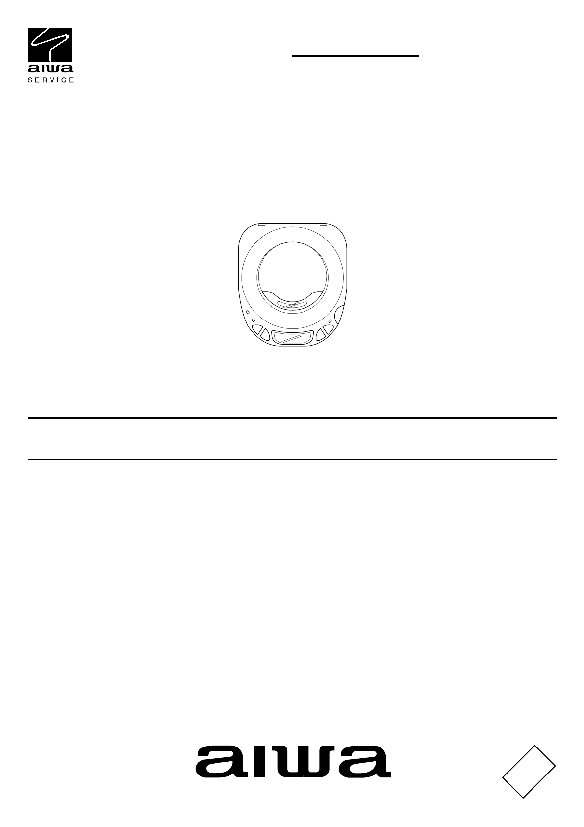
XP-V319
ALH1SK
SERVICE MANUAL
COMPACT DISC PLAYER
MODEL CODE : 86HR8-0117(B)
BASIC CD MECHANISM : DA23L
S/M Code No. 09-003-339-8N2
DATA
Page 2
PROTECTION OF EYES FROM LASER BEAM DURING SERVICING
This set employs laser. Therefore, be sure to follow carefully the
instructions below when servicing.
WARNING!
WHEN SERVICING, DO NOT APPROACH THE LASER EXIT
WITH THE EYE TOO CLOSELY. IN CASE IT IS NECESSARY TO
CONFIRM LASER BEAM EMISSION. BE SURE TO OBSERVE
FROM A DISTANCE OF MORE THAN 30cm FROM THE
SURFACE OF THE OBJECTIVE LENS ON THE OPTICAL
PICK-UP BLOCK.
Caution: Invisible laser radiation when
open and interlocks defeated avoid exposure to beam.
Advarsel:Usynling laserståling ved åbning,
når sikkerhedsafbrydere er ude af funktion.
Undgå udsættelse for stråling.
VAROITUS!
Laiteen Käyttäminen muulla kuin tässä käyttöohjeessa mainitulla tavalla saattaa altistaa käyt-täjän turvallisuusluokan 1 ylittävälle näkymättömälle lasersäteilylle.
VARNING!
Om apparaten används på annat sätt än vad som specificeras i
denna bruksanvising, kan användaren utsättas för osynling
laserstrålning, som överskrider gränsen för laserklass 1.
CAUTION
Use of controls or adjustments or performance of procedures
other than those specified herein may result in hazardous
radiation exposure.
ATTENTION
L'utilisation de commandes, réglages ou procédures autres que
ceux spécifiés peut entraîner une dangereuse exposition aux
radiations.
ADVARSEL!
Usynlig laserståling ved åbning, når sikkerhedsafbrydereer ude
af funktion. Undgå udsættelse for stråling.
This Compact Disc player is classified as a CLASS 1 LASER
product.
The CLASS 1 LASER PRODUCT label is located on the rear
exterior.
CLASS 1
KLASSE 1
LUOKAN 1
KLASS 1
LASER PRODUCT
LASER PRODUKT
LASER LAITE
LASER APPARAT
-2-
Page 3
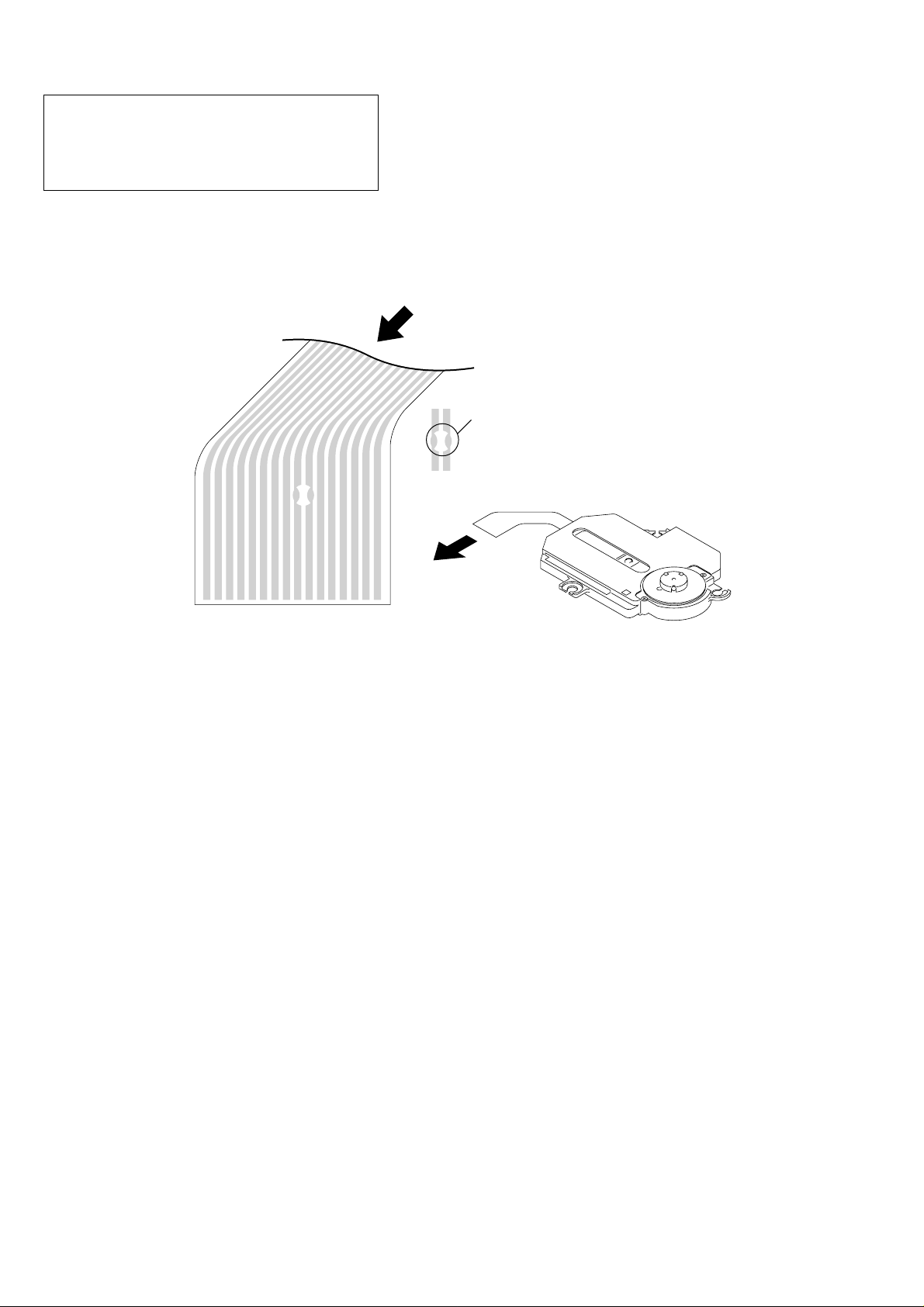
Precaution to replace Optical block
(SF-P200)
Body or clothes electrostatic potential could ruin
laser diode in the optical block. Be sure ground
body and workbench, and use care the clothes
do not touch the diode.
1) After the connection, remove solder shown in
the right figure.
:SOLDER
10 9
PICK UP ASSY
116
SF-P200
-3-
Page 4
SPECIFICATIONS
Design and specifications are subject to change without notice.
•
-4-
Page 5

ELECTRICAL MAIN PARTS LIST-1/2
REF. NO PART NO. KANRI DESCRIPTION
NO.
IC
87-A21-448-040 C-IC,BH6554FV
87-A21-083-040 C-IC,BH6508FS
87-A21-381-040 C-IC,LA9235M
87-A21-591-010 C-IC,LC78641NE-D
87-A21-085-040 C-IC,TA2120FN
8A-HC7-607-010 C-IC,UPD789406AGC-014-8BT
TRANSISTOR
89-211-323-080 C-TR,2SB1132R
87-A30-332-040 C-TR,CPH3106
87-A30-278-040 C-FET,2SK2980
87-A30-287-040 C-TR,DTC114TKA
87-A30-246-040 C-TR,2SA1037AK
86-NFZ-667-040 C-TR,DTC123JKA
89-416-643-080 C-TR,2SD1664R
89-324-123-080 C-TR,2SC2412K S
DIODE
87-A40-592-040 C-ZENER,HZM11NB2
87-A40-590-040 C-DIODE,HRW0202A
87-A40-554-040 C-DIODE,RB491D
87-A40-469-080 C-DIODE,HSM2838CTR
87-A40-836-040 C-ZENER,HZM6.2NB1
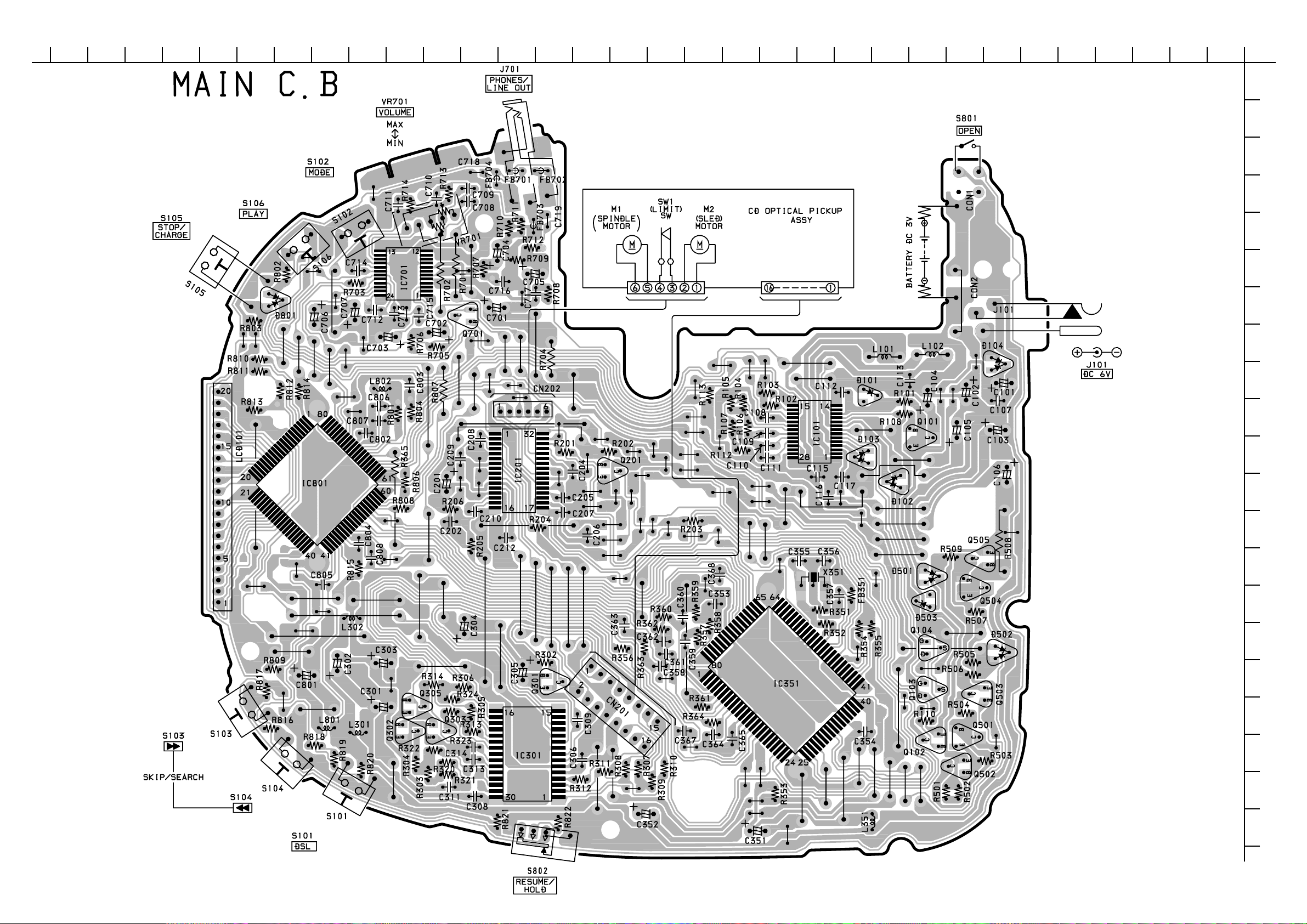
MAIN C.B
C101 87-010-553-040 CAP,E 47-16 GAS
C102 87-010-551-040 CAP,E 33-10 GAS
C103 87-A10-505-040 CAP,E 220-6.3 105 SF
C104 87-010-503-040 CAP,E 220-4 GAS
C105 87-010-498-040 CAP,E 10-16 GAS
C106 87-010-502-040 CAP ELECT GAS 100/4
C107 87-010-196-080 CHIP CAPACITOR,0.1-25
C108 87-012-145-080 CAP, CHIP S 270P CH
C109 87-010-198-080 CAP, CHIP 0.022
C110 87-A10-826-080 C-CAP,S 1-10 K B
C111 87-010-196-080 CHIP CAPACITOR,0.1-25
C112 87-010-196-080 CHIP CAPACITOR,0.1-25
C113 87-A10-826-080 C-CAP,S 1-10 K B
C115 87-010-196-080 CHIP CAPACITOR,0.1-25
C116 87-010-196-080 CHIP CAPACITOR,0.1-25
C117 87-010-196-080 CHIP CAPACITOR,0.1-25
C201 87-A10-505-040 CAP,E 220-6.3 105 SF
C202 87-010-175-080 CAP 560P
C204 87-010-213-080 C-CAP,S 0.015-50 B
C205 87-010-213-080 C-CAP,S 0.015-50 B
C206 87-A10-826-080 C-CAP,S 1-10 K B
C207 87-A10-826-080 C-CAP,S 1-10 K B
C208 87-010-177-080 C-CAP,S 820P-50 SL
C209 87-010-213-080 C-CAP,S 0.015-50 B
C210 87-010-213-080 C-CAP,S 0.015-50 B
C212 87-A10-826-080 C-CAP,S 1-10 K B
C301 87-016-557-040 CAP,E 100-6.3 SF
C302 87-010-502-040 CAP ELECT GAS 100/4
C303 87-016-557-040 CAP,E 100-6.3 SF
C304 87-010-502-040 CAP ELECT GAS 100/4
C305 87-010-501-040 E/CAP GAS 47-4
C306 87-010-196-080 CHIP CAPACITOR,0.1-25
C308 87-010-196-080 CHIP CAPACITOR,0.1-25
C309 87-010-178-080 CHIP CAP 1000P
C311 87-010-318-080 C-CAP,S 47P-50 CH
C313 87-A10-826-080 C-CAP,S 1-10 K B
C314 87-A10-201-080 C-CAP,S0.33-16 KB
C351 87-016-557-040 CAP,E 100-6.3 SF
C352 87-010-503-040 CAP,E 220-4 GAS
C353 87-A10-826-080 C-CAP,S 1-10 K B
REF. NO PART NO. KANRI DESCRIPTION
NO.
C354 87-010-196-080 CHIP CAPACITOR,0.1-25
C355 87-010-312-080 C-CAP,S 15P-50 CH
C356 87-010-312-080 C-CAP,S 15P-50 CH
C357 87-010-196-080 CHIP CAPACITOR,0.1-25
C358 87-010-322-080 C-CAP,S 100P-50 CH
C359 87-A10-369-080 C-CAP,S 0.47-16 K B
C360 87-016-669-080 C-CAP,S 0.1-25 K B
C361 87-010-322-080 C-CAP,S 100P-50 CH
C362 87-016-669-080 C-CAP,S 0.1-25 K B
C363 87-010-197-080 CAP, CHIP 0.01 DM
C364 87-016-369-080 C-CAP,S 0.033-25 B K
C365 87-010-322-080 C-CAP,S 100P-50 CH
C367 87-010-175-080 CAP 560P
C368 87-010-196-080 CHIP CAPACITOR,0.1-25
C701 87-010-501-040 E/CAP GAS 47-4
C702 87-010-495-040 CAP,E 2.2-50 GAS
C703 87-010-498-040 CAP,E 10-16 GAS
C704 87-010-503-040 CAP,E 220-4 GAS
C705 87-010-503-040 CAP,E 220-4 GAS
C706 87-010-498-040 CAP,E 10-16 GAS
C707 87-010-501-040 E/CAP GAS 47-4
C708 87-A10-826-080 C-CAP,S 1-10 K B
C709 87-A10-826-080 C-CAP,S 1-10 K B
C710 87-012-155-080 C-CAP 180P-50CH
C711 87-012-155-080 C-CAP 180P-50CH
C712 87-012-141-080 CHIP-CAPACITOR,0.22-16F
C713 87-010-196-080 CHIP CAPACITOR,0.1-25
C714 87-010-196-080 CHIP CAPACITOR,0.1-25
C715 87-010-196-080 CHIP CAPACITOR,0.1-25
C716 87-010-196-080 CHIP CAPACITOR,0.1-25
C717 87-010-196-080 CHIP CAPACITOR,0.1-25
C801 87-010-501-040 E/CAP GAS 47-4
C802 87-010-196-080 CHIP CAPACITOR,0.1-25
C803 87-010-196-080 CHIP CAPACITOR,0.1-25
C804 87-010-178-080 CHIP CAP 1000P
C805 87-010-322-080 C-CAP,S 100P-50 CH
C806 87-010-319-080 C-CAP,S 56P-50 CH
C807 87-010-319-080 C-CAP,S 56P-50 CH
C808 87-010-196-080 CHIP CAPACITOR,0.1-25
CN201 87-A61-104-010 CONN,16P H WHITE 52089-1610
CN202 87-009-411-010 CONN,6P ZH V
FB701 87-A50-623-080 C-COIL,BK2125HS102
FB702 87-A50-623-080 C-COIL,BK2125HS102
FB703 87-A50-623-080 C-COIL,BK2125HS102
FB704 87-A50-623-080 C-COIL,BK2125HS102
J101 87-A61-447-010 JACK,DC DJ26B BLK 6
J701 87-A61-446-010 JACK,3.5 GRN ST W/REM
L101 87-A50-574-010 COIL,100UH #7607
L102 87-A50-573-010 COIL,330UH LHL06NB
L301 87-A50-455-080 C-COIL,47UH-FSLB2520
L302 87-A50-501-080 C-COIL,10UH-FSLB2520
L351 87-A50-501-080 C-COIL,10UH-FSLB2520
L801 87-A50-501-080 C-COIL,10UH-FSLB2520
L802 87-A50-455-080 C-COIL,47UH-FSLB2520
LCD101 8A-HC7-602-010 LCD,AHC-7
R105 87-022-355-080 C-RES,S10K-1/10W F
R107 87-022-358-080 C-RES,S 18K-1/10W F
R307 87-022-202-080 C-RES,S33K 1/10WF
R308 87-022-202-080 C-RES,S33K 1/10WF
R309 87-022-202-080 C-RES,S33K 1/10WF
R310 87-022-202-080 C-RES,S33K 1/10WF
R311 87-022-364-080 C-RES,S 82K-1/10W F
R312 87-022-364-080 C-RES,S 82K-1/10W F
S101 87-A90-095-080 SW,TACT EVQ11G04M
S102 87-A90-095-080 SW,TACT EVQ11G04M
S103 87-A90-095-080 SW,TACT EVQ11G04M
S104 87-A90-095-080 SW,TACT EVQ11G04M
S105 87-A90-095-080 SW,TACT EVQ11G04M
S106 87-A90-095-080 SW,TACT EVQ11G04M
S801 87-A91-622-010 SW,MICRO PV1102
-5-
Page 6
ELECTRICAL MAIN PARTS LIST-2/2
REF. NO PART NO. KANRI DESCRIPTION
NO.
S802 87-A91-742-010 SW,SL 4-1-3 HSW2061-010010
VR701 87-A90-462-010 VR,RTRY 30KCX2 H RK14J12A0
X351 87-A70-202-080 C-VIB,CER 16.93MHZ CSACV-MXJ04
REF. NO PART NO. KANRI DESCRIPTION
NO.
• Regarding connectors, they are not stocked as they are not the initial order items.
The connectors are available after they are supplied from connector manufacturers upon the order is received.
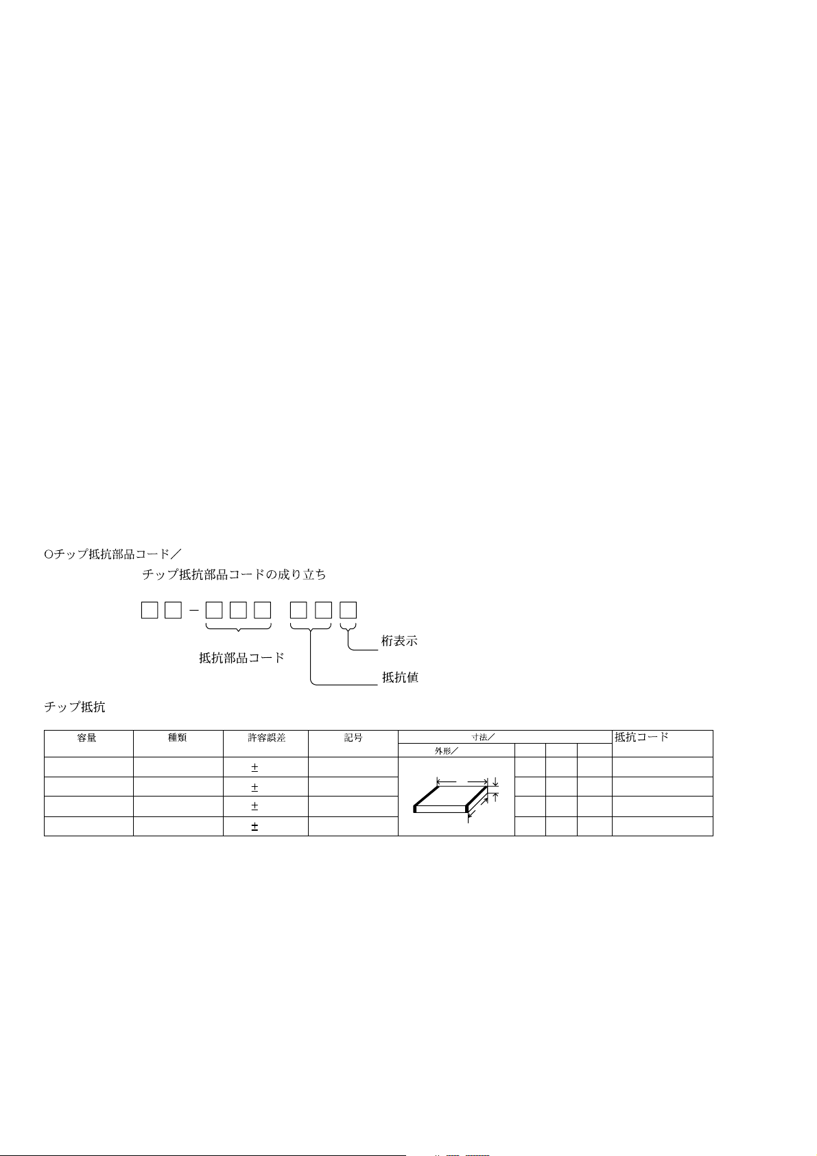
CHIP RESISTOR PART CODE
Chip Resistor Part Coding
88
A
Resistor Code
Chip resistor
Wattage Type Tolerance
1/16W 1005 5% CJ
1/16W
1/10W
1/8W
1608
2125
3216
5%
5%
5%
Symbol
Figure
Value of resistor
CJ
CJ
CJ
Form
L
W
Dimensions (mm)
LW t
1.0 0.5 0.35 104
t
1.6 0.8 0.45
2 1.25 0.45
1.6
0.55
3.2
Resistor Code
108
118
128
: A
: A
-6-
Page 7
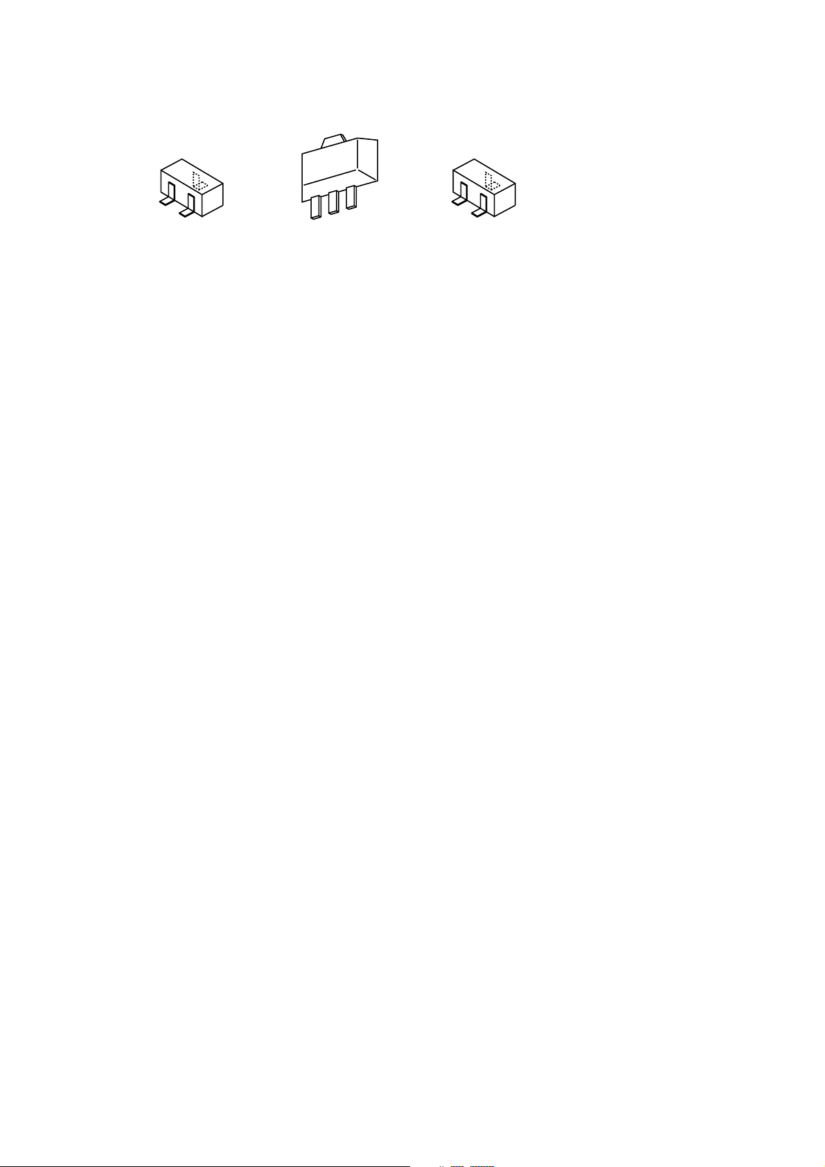
TRANSISTOR ILLUSTRATION-1/1
C
B
E
2SA1037
2SC2412
CPH3106
DTC114TK
DTC123JK
BCE
2SB1132
2SD1664
D
G
S
2SK2980
-7-
Page 8
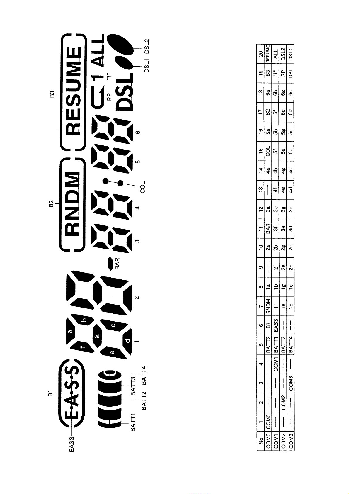
FL (AHC-7) GRID ASSIGNMENT/ANODE CONNECTION-1/1
GRID ASSIGNMENT
ANODE CONNECTION
-8-
Page 9
WIRING-1/1
101112131415161718192021222324
1234567892526272829303132
A
B
C
D
SF-P200
E
F
G
H
I
J
K
L
M
-9-
N
O
P
Q
R
S
T
U
Page 10

SCHEMATIC DIAGRAM-1/1
Z
-10-
Page 11

TEST MODE-1/3
IC101
IC351
IC701
IC201
IC801
IC301
27
Q305
RF
31
VC
TEST MODE SHORT LAND
-11-
Page 12

TEST MODE-2/3
The servo circuit of this model has been designed to be free of adjustments and controlled within the IC. Therefore, adjustments and disk judgement
are performed automatically every time the TOC is read out. The adjustment status of each servo inside the IC can be monitored in this test mode.
1. Startup procedure
1) Short the test land.
2) Insert the AC plug.
3) Press the STOP button. (The test mode starts.)
Note 1) The test mode is canceled by disconnecting the AC plug.
Note 2) The OPEN/CLOSE switch cannot be operated during the test mode.
2. Checking the RF level
Test point: RF & VC (Vref)
Test disk: TCD-782
Play back the disk and confirm that the RF waveform is in the following state:
0.8Vp-p or more
VOLT/DIV:200mV
TIME/DIV:0.5us
3. Checking each servo
The adjustment values of each servo can be checked by pressing the MODE button repeatedly during playback. The switching
procedure is as follows.
Check mode OFF™Vref offset (RO)™focus offset (FO)™tracking offset (TO)™tracking balance (TB)™tracking gain (TG) ™
focus gain (FG)™focus bias (FB)™check mode OFF
Example: Tracking offset (TO) Adjustment value™F5
RNDM RESUME
1
DSL
Tracking offset
* Adjustment values are indicated in hexadecimal.
When displaying each mode on the LCD and pressing the PLAY button in the STOP status, the center value is displayed on the LCD.
After the disk starts rotating, the adjustment value that was set during automatic adjustment is displayed. The display range of the
center values and adjustment values of each mode are as follows. There are 256 steps for displaying the values of all modes.
Center value
1) Vref offset (RO)
2) Focus offset (FO)
3) Tracking offset (TO)
4) Tracking balance (TB)
5) Tracking gain (TG)
6) Focus gain (FG)
7) Focus bias (FB)
Adjustment value
Center value
00
00
00
80
40
40
00
Display range
80-7F
80-7F
80-7F
00-FF
00-FF
00-FF
80-7F
-12-
Page 13

TEST MODE-3/3
4. Amount of change of jitter
The amount of change of jitter is displayed in the focus bias check mode. The displayed value has 256 steps from 00 to FF.
Example: focus bias (FB) Adjustment value™00 Jitter value™FD
RNDM RESUME
1
DSL
Tracking offset Adjustment value
* Adjustment values and jitter values are indicated in hexadecimal.
Jitter value
-13-
Page 14

WAVE FORM-1/1
1 IC301 Pin ≥ VOLT/DIV: 0.2V
RF TIME/DIV: 0.5µS
2 IC301 Pin * VOLT/DIV: 0.2V
TE TIME/DIV: 50µS
3 IC301 Pin ¡ VOLT/DIV: 0.1V
FE- TIME/DIV: 2mS
7 IC351 Pin ∞ VOLT/DIV: 0.1V
SPDO TIME/DIV: 5mS
4 IC351 Pin VOLT/DIV: 1V
XOUT TIME/DIV: 50mS
5 IC801 Pin VOLT/DIV: 1V
X1 TIME/DIV: 0.2µS
6 IC351 Pin VOLT/DIV: 2V
LRSY TIME/DIV: 5µS
52
f=16.93MHz
69
f=4.2MHz
57
f=44.1kHz
-14-
Page 15

IC BLOCK DIAGRAM-1/1
IC, BH6508FS
MUTE
4
IC, BH6554FV
POW
IN4 CN4CLK CN3
GND
IN1 CN1CT
OUT
4R
POW
GND
POW
VCC
OUT
1F
OUT
4R
POW
VCC
POW
GND
OUT
1R
OUT
3R
POW
GND
POW
VCC
OUT
2R
OUT
3F
POW
VCC
POW
GND
OUT
2F
POW
GND
IN3
VCC
VG
VREF
IN2CN2
IC, TA2120FN
IN-L IN-R
-15-
Page 16

IC DESCRIPTION-1/3 (LC78641NE-D)-1/3
Pin No. Pin Name I/O Description
1
PDO1
Internal VCD control phase comparator output pin.
O
10
11
12
13
14
15
16
17
2
3
4
5
6
7
8
9
PDO2
VVSS
PCKIST
VVDD
FR
HFL
SLCIST
SLCO
EFMIN
JITTV
JITTC
BH
PH (RFENV)
FE
TE
VREF
—
—
Internal VCD control phase comparator output pin. OFF for rough servo, ON for phase servo.
O
Internal VCD ground pin.
PDO output current adjustment resistor connection pin. (pull up)
I
Internal VCD power supply pin. (2000pF or more path controller to be inserted at a point nearer
to the pin between this pin and GND)
VCD frequency range adjustment resistor connection pin. (pull up)
I
Mirror detection signal input pin.
I
SLCO output current adjustment resistor connection pin. (pull up)
I
Control outout.
O
EFM signal input pin.
I
Jitter detection monitor pin.
O
Jitter detection adjustment pin.
O
BH signal input pin. A/D input. (Must be connected to OV when unused)
I
PH signal or RFENV signal input pin. A/D input.
I
FE signal input pin. A/D input.
I
TE signal input pin. A/D input.
I
VREF input pin. A/D input.
I
18
19
20
21
22
23
24
25
26
27
28
29
30
31
32
33
ADAVDD
ADAVSS
PHREF
BHREF
TBLO
TDO
FDO
SPDO
SLDO
DVREF/FG
LASER
CONT1
CONT2
CONT3
CONT4
CONT5
—
—
O
O
O
O
O
O
O
I/O
O
I/O
I/O
I/O
I/O
I/O
Servo A/D, D/A power supply pin. (2000pF or more path controller to be inserted at a point
nearer to the pin between this pin and GND)
Servo A/D, D/A ground pin.
PH reference output pin. D/A output. (Not connected)
BH reference output pin. D/A output. (Not connected)
Tracking balance output pin. D/A output.
Tracking control output pin. D/A output.
Focus control output pin. D/A output.
Spindle control output pin. D/A output.
Thread control output pin. D/A output.
Output driver VREF output pin. Input FG signal input pin. (Must be connected to OV when
unused) (Not connected)
Laser ON/OFF control pin.
General-purpose input/output pin 1. (Not connected)
General-purpose input/output pin 2. (Not connected)
General-purpose input/output pin 3. (Not connected)
General-purpose input/output pin 4.
General-purpose input/output pin 5.
34
35
36
PCK
C2F
VDD
—
EFM data playback clock monitor pin. Average 4.3218MHz when the phase is locked.
O
(Not connected)
C2 flag output pin. (Not connected)
O
Digital power supply pin. (2000pF or more path controller to be inserted at a point nearer to the
pin between this pin and GND)
-16-
Page 17

IC DESCRIPTION-1/3 (LC78641NE-D)-2/3
Pin No. Pin Name I/O Description
37
DOUT
Digital OUT output pin. (EIAJ format) (Not connected)
O
38
39
40
41
42
43
44
45
46
47
48
49
50
FSX
EFLG
TEST
EMPH
MUTEL
MUTER
LVDD
LCHO
LVSS
RVSS
RCHO
RVDD
XVDD
O
O
I/O
O
O
—
O
—
—
O
—
—
Output pin for the 7.35kHz synchronization signal divided from the crystal osillator.
(Not connected)
(Not connected)
C1 C2 error correction monitor pin. Test input pin. Must be connected to OV.
I
Emphasis pin. Which becomes an input pin after reset and can becontrolled externally.
This becomes an emphasis monitor pin under control by command. (Not connected)
L channnel mute output pin.
R channel mute output pin.
L channel power supply pin. (2000pF or more path controller to be inserted at a point
nearer to the pin between this pin and GND)
L channel output pin.
L channel ground pin, Must be connected to 0V.
R channel ground pin, Must be connected to 0V.
R channel output pin.
R channel power supply pin. (2000pF or more path controller to be inserted at a point
nearer to the pin between this pin and GND)
Crystal oscillator power supply pin. (2000pF or more path controller to be inserted at a
point nearer to the pin between this pin and GND)
51
52
53
54
55
56
57
58
59
60
61
62
63
64
65
66
XIN
XOUT
XVSS
ASLRCK
ASDACK
ASDFIN
LRSY
DATACK
DATA
16M
SFSY
SBSY
PW
SBCK
CE
CL
I
Connections for a 16.9344MHz crystal oscillator pin.
O
Crystal oscillator ground pin. Must be connected to 0V.
—
L/R clock input pin. (Must be connected to 0V when unused)
I
Bit clock input pin. (Must be connected to 0V when unused)
I
L/R channel data input pin. (Must be connected to 0V when unused)
I
L/R clock output pin.
O
Bit clock output pin. (Not connected)
O
L/R channel data output pin. (Not connected)
O
16.9344MHz output pin. (Not connected)
O
Subcode frame synchronization signal output pin. This signal falls when the subcode is
O
in the standby state. (Not connected)
Subcode clock synchronization signal output pin. (Not connected)
O
Subcode P, Q, R, S, T, U and W output pin. (Not connected)
O
Subcode readout clock input pin.
I
Chip enable signal input pin.
I
Data transfer clock input pin.
I
67
68
69
70
71
DI
DO
INT
WRQ
RES
Data input pin.
I
Data output pin.
O
Interruption signal output pin. (Not connected)
O
Interruption signal output pin.
O
Reset input pin. This pin must be set low briefly after power is first applied.
I
-17-
Page 18

IC DESCRIPTION-1/3 (LC78641NE-D)-3/3
Pin No. Pin Name I/O Description
72
DRF
Focus ON detect pin.
O
73
74
75
76
77
78
79
80
VDD5V
VSS
CONT6
CONT7
V/P
FSEQ
DFECT
EFMO
—
—
I/O
I/O
O
O
I/O
O
Microprocessor interface power supply. (2000pF or more path controller to be inserted
at a point nearer to the pin between this pin and GND)
Digital ground pin. Must be connected to 0V.
General-purpose input/output pin 6. (Not connected)
General-pirpose input/output pin 7. (Not connected)
Rough servo/phase control automatic switching monitor output pin. “H” for rough
servo and “L” for phase servo. (Not connected)
Synchronization signal detection output pin. Outputs a high level when the
synchronization signal detected from the EFM signal and the internally generated
synchronization signal agree. (Not connected)
Defect pin. Which becomes an input pin after reset and can be controlled externally.
This becomes the defect monitor pin under control by command. (Not connected)
EFM signal output pin. (Not connected)
-18-
Page 19

IC DESCRIPTION-2/3 (µPD789406AGC-014)-1/2
Pin No. Pin Name I/O Description
1
VDD1
—
Positive polarity power supply (except for port section).
2
3-5
6
7-10
11-26
27-30
31
32
33
34-37
38
39
40
41
42
43
44
BIAS
VLC0-VLC2
VSS1
COM0-COM3
S0-S15
P93-P90
P87
P86
P85
P84-P81
P80
AVDD
AVREF
ANI6/P66
ANI5/P65
ANI4/P64
ANI3/P63
—
—
—
—
—
Feeding the LCD drive power supply voltage.
LCD drive power supply voltage.
Ground potential (except for port section).
Common signal output from LCD controller/driver.
O
Segment signal output from LCD controller/driver.
O
P93-P90. (Signal name: COM3-COM0). COM3-COM0 relay port.
I
P87. (Signal name: TSTMOD) (Connected to Ground). L: TEST MODE.
I
P86. (Signal name: CDRW). L: CD-RW.
O
P85. (Signal name: AGON). H: AGON.
O
P84-P81. (Not connected)
O
P80. (Signal name: SHOCK) (Connected to Ground). L: Gain-up circuit operation during shock.
I
A/D comparator analog power supply.
A/D comparator reference voltage.
Signal name: OPEN. OPEN switch. Lid opens at 1 Dh or more.
I
Signal name: K-HLD. RESUME/HOLD key accepts.
I
Signal name: K-OTH. BS, FS, MODE, DSL key accepts.
I
Signal name: VDIN. Battery voltage monitoring.
I
45
46
47
48
49
50
51
52
53
54
55
56
57
58
59
60
61
ANI2/P62
ANI1/P61
ANI0/P60
AVSS
P27
P26
P25/INTP1
P24
P23/TO2
P22
P21
P20
P53
P52
P51
P50
P03
—
Signal name: RMC. Remote control key accepts.
I
Signal name: MUTLR. Zero data detection. MUTE at CDH or more.
I
Connected to Ground.
I
A/D comparator ground potential.
Signal name: DRF. Focus ON detection signal.
I
Not connected.
O
Signal name: WRQ. Interrupt signal from DSP.
I
Signal name: DO. Serial data reception from DSP.
I
Signal name: BEEP. Square wave output for BEEP sound.
O
Signal name: DI. Data output to DSP.
O
Signal name: CE. Chip enable output to DSP.
O
Signal name: CL. Serial clock output to DSP.
O
Signal name: K-STOP. H: When STOP button is pressed.
I
Signal name: K-PLAY. H: When PLAY button is pressed.
I
Signal name: ACDECT. H: AC adapter is detected.
I
Not connected.
O
Signal name: SPCON. H: Spindle stop.
O
62
63
64
65
66
67
P02
P01
P00
P47
P46
_____________
RESET
Signal name: SLCON. H: Sled stop.
O
Signal name: LSW. L: Sled inner circumference limit.
I
Signal name: APOFF. L: DC-DC CONV OFF.
O
Not connected.
O
Signal name: XRST. L: DSP reset.
O
System reset input.
I
-19-
Page 20

IC DESCRIPTION-2/3 (µPD789406AGC-014)-2/2
Pin No. Pin Name I/O Description
68
69
X2
X1
—
Terminal to connect external crystal for main system clock oscillation.
I
70
71
72
73
74
75
76
77
78
79, 80
VSS0
VDD0
XT2
XT1
IC/VPP
P45
P44
P43
P42
P41, P40
—
—
—
—
Ground potential of port section.
Positive polarity power supply for port section.
Not connected.
I
Terminal to connect external crystal for sub system clock oscillation. (Connected to Ground)
This pin is internally connected. Connect this pin directly to Vss0 or Vss1.
O
Signal name: SDBY. H: Output amplifier operates.
O
Signal name: MUTE. H: MUTE ON (Output amplifier).
O
Signal name: DSL1. L: DSL ON (Step 1).
O
Signal name: DSL2. H: DSL ON (Step 2) (When DSL1 is H).
O
Not connected.
-20-
Page 21

IC DESCRIPTION-3/3 (LA9253M)-1/1
Pin No. Pin Name I/O Description
1
FIN1
I
10
11
12
13
14
15
16
17
18
2
3
4
5
6
7
8
9
FIN2
TIN1
TIN2
REF1
VREF
LDS
LDD
GND
LDOF
ODRV
AGON
EFBL
TESO
TESI
TES
HFL
TE
—
I
Pick-up signal input.
I
I
Pin designed for reference voltage.
I
Reference voltage output.
O
APC monitor voltage input.
I
APC output.
O
GND.
Laser OFF pin. (H: ON L: OFF)
I
Speed switch pin. (H: double L: normal speed)
I
AGC ON pin. (H: ON L: OFF)
I
FE balance adjustment pin.
I
TE signal output for TES. (Not connected)
O
TE input for TES formation. (Not connected)
I
TES output. (Not connected)
O
HFL signal output.
O
TE signal output.
O
19
20
21
22
23
24
25
26
27
28
29
30
TE-
FE
FE-
RFEV
N/C
BH
PH
N/C
RF
RF-
RFSW
VCC
—
—
—
Minus input for TE gain design.
I
FE signal output.
O
Minus input for FE gain design.
I
RF envelop signal output.
O
Pin N/C.
Capasitance connection pin for RF bottom clamp.
I
Capasitance connection pin for RF gain design.
I
Pin N/C.
RF signal output.
O
Minus input for RF signal gain design.
I
Switch for equalizer design when RF has double speed.
I
Power supply.
-21-
Page 22

MECHANICAL EXPLODED VIEW-1/1
8
8
1
LCD
9
PWB
DA23L
8
10
B
12
11
2
3
4
5
7
13
6
a
A
15
14
a
-22-
Page 23

MECHANICAL PARTS LIST-1/1
REF. NO PART NO. KANRI DESCRIPTION
1 8A-HC7-007-010 WINDOW,CD
2 8A-HC7-138-010 WINDOW,DISPLAY 319
3 8A-HC7-017-110 LID ASSY,CD
4 85-HC6-205-110 SHAFT,LID(300) HK
5 8A-HC7-204-010 SPR-T,OPEN
6 8A-HC7-018-110 LEVER,OPEN
7 8A-HC7-015-310 CABI ASSY,CENTER
8 8Z-HC1-225-010 DMPR,MECHA(SP)
9 8A-HC7-201-010 GUIDE,LCD
10 8A-HC7-207-010 BAT-CONTACT,(-) (HK)
11 8A-HC7-206-010 BAT-CONTACT,(+) (HK)
12 87-HC8-205-010 BAT-CONTACT,(+)(-)
13 8A-HC7-012-010 KNOB,SL HOLD
14 8A-HC7-016-010 CABI ASSY,BOTTOM
15 88-HC6-021-010 FOOT, DIA10
A 87-067-869-010 V+1.7-8 HL BLK
B 87-067-868-010 V+1.7-4 HL BLK
NO.
-23-
Page 24

COLOR NAME TABLE
Basic color symbol Color Basic color symbol Color Basic color symbol Color
B Black C Cream D Orange
G Green H Gray L Blue
LT Transparent Blue N Gold P Pink
R Red S Silver ST Titan Silver
T Brown V Violet W White
WT Transparent White Y Yellow YT Transparent Yellow
LM Metallic Blue LL Light Blue GT Transparent Green
LD Dark Blue DT Transparent Orange GM Metallic Green
YM Metallic Yellow DM Metallic Orange PT Transparent Pink
LA Aqua Blue GL Light Green
-24-
Page 25

CD MECHANISM EXPLODED VIEW-1/1
D
D
2
4
9
A
3
5
1
7
8
C
6
B
-25-
10
Page 26

CD MECHANISM PARTS LIST-1/1
REF. NO PART NO. KANRI DESCRIPTION
1 S0-A41-A20-600 PICKUP LASER ASSY
2 SM-10A-108-001 MOTOR ASSY SPINDLE
3 S0-M10-A10-900 MOTOR SLED ASSY
4 S2-311-A12-200 CHASSIS
5 S2-511-A23-200 GEAR MIDDLE
6 S2-511-A23-100 GEAR,SCREW
7 S2-511-A23-400 GEAR,RACK
8 S2-511-A07-900 SPINDLE SCREW
9 S4-S13-A00-200 SW,LEAF
10 S2-451-A18-100 HOLDER GEAR
A SS-EXE-A04-000 SCR PAN PCS 1.4-2.2
B SS-GXE-A00-300 SPECIAL SCREW
C SS-EXE-A14-100 SPECIAL SCREW
D SS-GXE-A00-202 SPECIAL SCREW M1.7-4.0
NO.
-26-
Page 27

ACCESSORIES/PACKAGE LIST-1/1
REF. NO PART NO. KANRI DESCRIPTION
!
1 87-B30-285-110 AC ADAPTOR,AC-D603HRNC
2 87-B30-326-010 HEADPHONE,HP-M048
3 8A-HC7-944-010 IB,CCE
!
4 87-A91-017-010 PLUG,CONVERSION JT-0476
NO.
-27-
Page 28

2–11, IKENOHATA 1–CHOME, TAITO-KU, TOKYO 110-8710, JAPAN TEL:03 (3827) 3111
737004
Printed in Singapore
 Loading...