

Page 1
XP-R110
XP-R210
ALH
ALH,AU
AHC,AHK,AHR
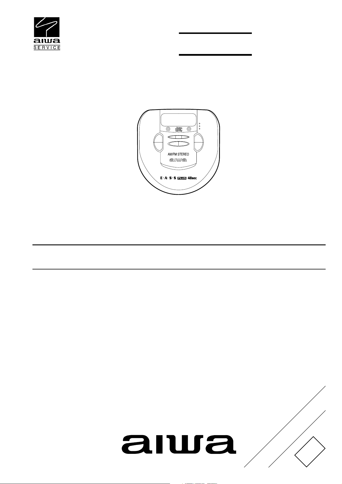
SERVICE MANUAL
COMPACT DISC PLAYER
• This Service Manual is the “Revision Publishing” and replaces “Simple Manual”
of XP-R110<ALH>(S/M Code No. 09-001-426-4T1) and XP-R210<AU,ALH>
(S/M Code No. 09-001-426-3T1) and XP-R210<AHC,AHK,AHR>
(S/M Code No. 09-001-426-3T2).
BASIC CD MECHANISM: DA23L
S/M Code No. 09-003-426-3R1
REVISION
DATA
Page 2

SPECIFICATIONS
Tracking system 3-beam laser
Laser pickup Semiconductor laser
D/A conversion 4-times oversampling digital
filter + 1-bit DAC
Frequency Response 20 – 20,000 Hz (47 K ohms)
Output PHONES/LINE OUT jack
(stereo mini-jack)
Frequency range AM: 531/530 kHz - 1,602/
1,710 kHz (9 kHz/10 kHz steps)
FM: 87.5 - 108 MHz
Maximum output 12 mW + 12 mW
( EIAJ 16 ohms at 1 kHz)
500 mV (47 k ohms at 1 kHz)
Power supply DC 3 V using two LR6 (size AA)
alkaline batteries
DC 2.4 V using two commercially
avaiable (Ni-Cd 1.2 V 700 mAh)
rechargeable batteries
DC 2.4 V using two supplied
rechargeable batteries<AHK>
AC house current using the
supplied AC adaptor
Maximum outside dimensions
Weight Approx. 225 g (7.9 oz.)
AC Adaptor AC-D603 HC
Rated input AC 220 V, 50 Hz<AHC>
• Design and specifications are subject to change without
notice.
128 (W) x 31.2 (H) x
129.5 (D) mm (excluding
projecting parts and controls)
1
/8 x 11/4 x 51/8 in.)
(5
(excluding batteries)
AC 120 V, 60 Hz<AU>
AC 230 V, 50 Hz<AHK>
115/230 V AC, switchable,
50/ 60 Hz<AHR>
For the customer in Argentina
AC-D603 HA: 230 V AC, 50 Hz
For the customer except in Argentina
AC-D603 HR: 115/230 V AC, switchable,
50/60 Hz<ALH>
ACCESSORIES / PACKAGE LIST
REF. NO. DESCRIPTIONPART NO.
1 8A-HC1-903-010 IB,HC(ECK)S<210AHC>
1 8A-HC1-910-010 IB,HK(ECH)S<210AHK>
1 8A-HC1-902-010 IB,HR(ECA)S<210AHR>
1 8A-HC1-904-010 IB,LH(3L)S<210ALH>
1 8A-HCB-904-010 IB,LH(3L)S<110ALH>
1 8A-HC1-901-010 IB,U(E)S<210AU>
1 8A-HC1-909-010 IB,U(F)S<210AU>
1 8A-HC1-908-010 IB,U(S)S<210AU>
2 87-A90-312-010 PLUG,CONVERSION WTN-1157R1<210ALH,210AHR,110ALH>
3 87-B30-141-010 BAT,NB-301 NC(2PCS)<210AHK>
4 87-B30-224-010 HEADPHONE,HP-M033<210AU>
4 87-B30-265-010 HEADPHONE,HP-M043<EXCEPT 210AU>
5 87-B30-286-010 AC ADAPTOR,AC-D603HCNC<210AHC>
5 87-B30-285-010 AC ADAPTOR,AC-D603HRNC<210ALH,210AHR,110ALH>
5 87-B30-284-010 AC ADAPTOR,AC-D603KNC<210AHK>
5 87-B30-282-010 AC ADAPTOR,AC-D603UNC<210AU>
KANRI
NO.
- 2 -
Page 3
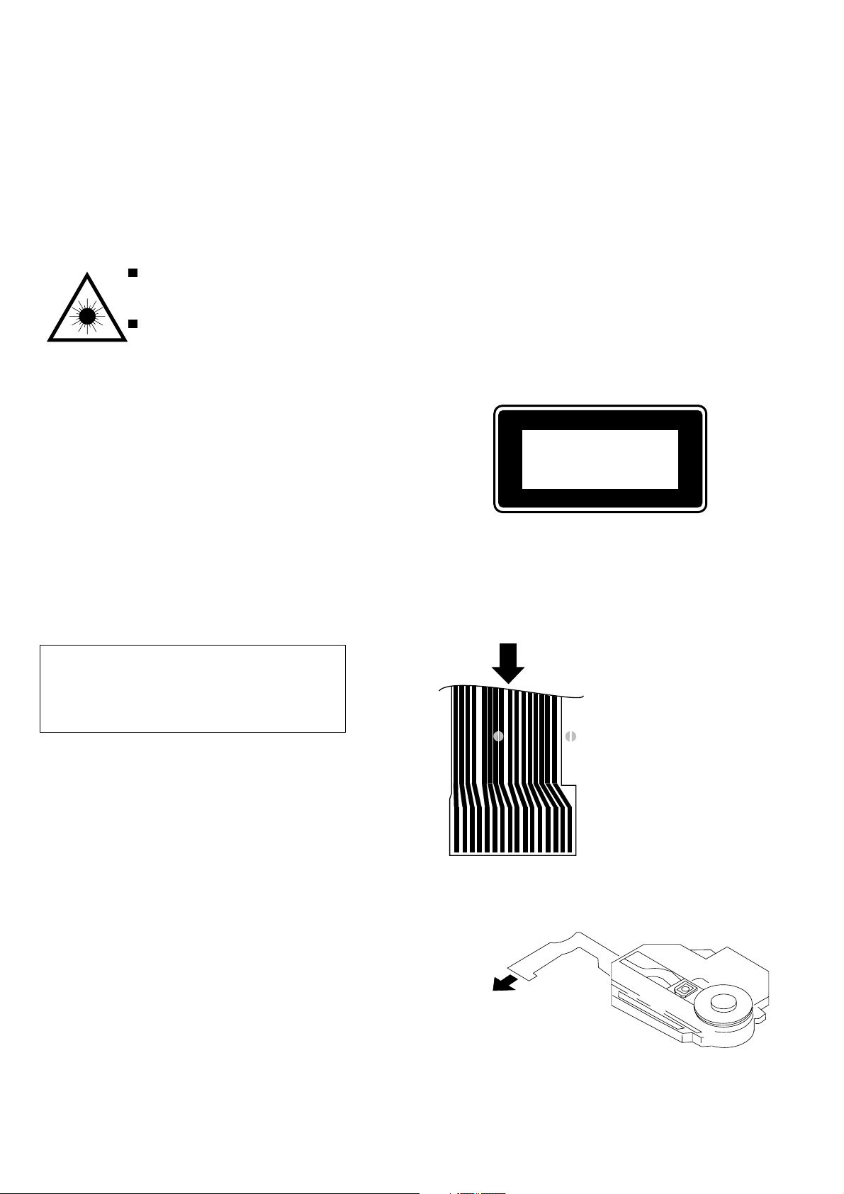
PROTECTION OF EYES FROM LASER BEAM DURING SERVICING
This set employs laser. Therefore, be sure to follow carefully the
instructions below when servicing.
WARNING!
WHEN SERVICING, DO NOT APPROACH THE LASER EXIT
WITH THE EYE TOO CLOSELY. IN CASE IT IS NECESSARY TO
CONFIRM LASER BEAM EMISSION. BE SURE TO OBSERVE
FROM A DISTANCE OF MORE THAN 30cm FROM THE
SURFACE OF THE OBJECTIVE LENS ON THE OPTICAL
PICK-UP BLOCK.
Caution: Invisible laser radiation when
open and interlocks defeated avoid expo-
sure to beam.
Advarsel:Usynling laserståling ved åbning,
når sikkerhedsafbrydere er ude af funktion.
Undgå udsættelse for stråling.
VAROITUS!
Laiteen Käyttäminen muulla kuin tässä käyttöohjeessa mainit-
ulla tavalla saattaa altistaa käyt-täjän turvallisuusluokan 1 ylit-
tävälle näkymättömälle lasersäteilylle.
VARNING!
Om apparaten används på annat sätt än vad som specificeras i
denna bruksanvising, kan användaren utsättas för osynling
laserstrålning, som överskrider gränsen för laserklass 1.
CAUTION
Use of controls or adjustments or performance of procedures
other than those specified herein may result in hazardous
radiation exposure.
ATTENTION
L'utilisation de commandes, réglages ou procédures autres que
ceux spécifiés peut entraîner une dangereuse exposition aux
radiations.
ADVARSEL!
Usynlig laserståling ved åbning, når sikkerhedsafbrydereer ude
af funktion. Undgå udsættelse for stråling.
This Compact Disc player is classified as a CLASS 1 LASER
product.
The CLASS 1 LASER PRODUCT label is located on the rear
exterior.
CLASS 1
KLASSE 1
LUOKAN 1
KLASS 1
LASER PRODUCT
LASER PRODUKT
LASER LAITE
LASER APPARAT
Precaution to replace Optical block
(SF-P200)
Body or clothes electrostatic potential could ruin
laser diode in the optical block. Be sure ground
body and workbench, and use care the clothes
do not touch the diode.
1) After the connection, remove solder shown in
the right figure.
: SOLDER
910 15161
- 3 -
PICK UP ASSY
Page 4

ELETRICAL MAIN PARTS LIST
REF. NO. DESCRIPTIONPART NO.
NO.
IC
87-A21-082-040 C-IC,BA6655AFV
8A-HC1-603-010 C-IC,MN101C439-AB
87-A21-446-010 C-IC,MN662782RPT1
87-A21-561-040 C-IC,MSM51V17400D-SJ<EXCEPT 110ALH>
87-A21-578-040 C-IC,AN8838NSB
87-A21-543-040 C-IC,NJU7012
87-A21-521-040 C-IC,BH6517FS
87-A21-085-040 C-IC,TA2120FN
87-A21-558-040 C-IC,LA1827V-TLM
87-A20-124-080 IC, TK11823
87-A21-559-040 C-IC,LC72121V-D-TLM
8A-HC1-604-010 C-IC,UPD789405AGK-A12-9EU
87-A21-030-040 C-IC,S-93C46AMFN
TRANSISTOR
87-026-608-080 C-TR,DTC 123 JK
87-A30-075-080 C-TR,2SA1235F
89-211-323-080 C-TR,2SB1132R
89-416-643-080 C-TR,2SD1664R
87-A30-076-080 C-TR,2SC3052F
89-113-695-680 C-TR,2SA1369G/H
87-A30-332-040 C-TR,CPH3106
87-A30-333-040 C-TR,CPH3206
87-A30-378-040 C-TR,UMG4N
87-026-210-040 C-TR,DTC144EK
87-A30-246-040 C-TR,2SA1037AK
87-A30-336-040 C-TR,UMH4N
87-026-233-080 TR,DTA114TK-TP
87-026-239-080 TR,DTC114TK (0.2W)
87-A30-377-040 C-TR,2SB815B7
89-324-121-080 C-TR,2SC2412K
87-026-235-080 CHIP-TR,DTC114EK
87-A30-328-040 C-TR,IMX9
87-026-210-080 CHIP-TR,DTC144EK
89-113-625-080 TR,2SA1362GR(120MHZ,0.
87-026-297-080 TR,DTA144TK
89-324-123-080 C-TR,2SC2412K S
89-327-143-080 TR,2SC2714 (0.1W)
89-503-025-080 CHIP FET,2SK302 GR
DIODE
87-A40-614-040 C-DIODE,SFPB-72
87-A40-469-080 C-DIODE,HSM2838CTR
87-A40-592-040 C-ZENER,HZM11NB2
87-A40-469-040 C-DIODE,HSM2838CTR
87-A40-590-040 C-DIODE,HRW0202A
87-020-331-080 CHIP-DIODE,DAN202K
MAIN C.B
C101 87-012-286-080 CAP, U 0.01-25
C102 87-A11-031-080 C-CAP,E 100-16 M WX
C103 87-012-286-080 CAP, U 0.01-25
C104 87-016-367-080 C-CAP,E 47-6.3
C201 87-016-431-080 C-CAP,E 220-4 5.5N
C202 87-012-274-080 CHIP CAP,U 1000P-50B
C203 87-012-286-080 CAP, U 0.01-25
C204 87-016-430-080 C-CAP,E 100-6.3 5.5N
C205 83-HC3-635-080 C-CAP,E 220-6.3 WF
C206 87-A12-159-080 C-CAP, 10-6.3 K B GRM42-6
C207 87-010-831-080 C-CAP,U,0.1-16F
C208 87-010-831-080 C-CAP,U,0.1-16F
C209 87-012-172-080 CAPACITOR CHIP U 10P CH
C210 87-012-195-080 C-CAP,U 100P-50CH
C211 87-A10-047-080 C-CAP,U 1-10 Z F
C212 87-012-188-080 C-CAP,U 47P-50 CH
REF. NO. DESCRIPTIONPART NO.KANRI
C213 87-A10-047-080 C-CAP,U 1-10 Z F
C214 87-010-831-080 C-CAP,U,0.1-16F
C215 87-A11-246-080 C-CAP,S 4.7-6.3 M B
C216 87-A11-246-080 C-CAP,S 4.7-6.3 M B
C217 87-010-831-080 C-CAP,U,0.1-16F
C301 87-016-426-080 C-CAP,E 47-4 5.5N
C302 87-012-286-080 C-CAP,U 0.01-25 K B
C303 87-012-274-080 C-CAP,U 1000P-50 K B<EXCEPT 110ALH>
C303 87-010-831-080 C-CAP,U,0.1-16F<110ALH>
C304 87-010-831-080 C-CAP,U,0.1-16F
C305 87-012-286-080 C-CAP,U 0.01-25 K B
C306 87-012-286-080 C-CAP,U 0.01-25 K B
C307 87-012-286-080 CAP, U 0.01-25
C309 87-016-430-080 C-CAP,E 100-6.3 5.5N
C310 87-012-286-080 CAP, U 0.01-25
C311 87-012-274-080 CHIP CAP,U 1000P-50B
C401 87-016-430-080 C-CAP,E 100-6.3 5.5N
C402 87-010-831-080 C-CAP,U,0.1-16F
C403 87-016-085-080 CAP,E 1000-6.3PF
C404 87-010-831-080 C-CAP,U,0.1-16F
C405 87-A10-260-080 C-CAP,U 0.1-16 K B
C406 87-012-273-080 C-CAP,U 820P-50 B
C407 87-010-787-080 CAP, U 0.022-25
C408 87-A10-260-080 C-CAP,U 0.1-16 K B
C409 87-A10-827-080 C-CAP,U 0.47-6.3 K B
C410 87-012-286-080 CAP, U 0.01-25
C411 87-010-831-080 C-CAP,U,0.1-16F
C412 87-016-429-080 C-CAP,E 100-4 5.5N
C413 87-010-831-080 C-CAP,U,0.1-16F
C415 87-010-831-080 C-CAP,U,0.1-16F
C420 87-010-831-080 C-CAP,U,0.1-16F
C421 87-010-831-080 C-CAP,U,0.1-16F
C422 87-010-831-080 C-CAP,U,0.1-16F
C423 87-010-831-080 C-CAP,U,0.1-16F
C451 87-010-831-080 C-CAP,U,0.1-16F<EXCEPT 110ALH>
C502 87-010-831-080 C-CAP,U,0.1-16F
C504 87-010-831-080 C-CAP,U 0.1-16F
C505 87-A11-228-080 C-CAP,U 0.027-25 K B
C506 87-012-199-080 CAP 220P
C507 87-012-193-080 C-CAP,U 82P-50 CH
C508 87-012-193-080 C-CAP,U 82P-50 CH
C509 87-012-193-080 C-CAP,U 82P-50 CH
C510 87-016-429-080 C-CAP,E 100-4 M WX
C511 87-010-831-080 C-CAP,U 0.1-16F
C512 87-016-426-080 C-CAP,E 47-4 5.5N
C513 87-010-831-080 C-CAP,U 0.1-16F
C514 87-A11-228-080 C-CAP,U 0.027-25 K B
C515 87-A11-228-080 C-CAP,U 0.027-25 K B
C516 87-A10-260-080 C-CAP,U 0.1-16 K B
C518 87-012-176-080 CAP 15P
C520 87-016-426-080 C-CAP,E 47-4 5.5N
C521 87-012-274-080 CHIP CAP,U 1000P-50B
C522 87-A10-047-080 C-CAP,U 1-10 Z F
C523 87-A10-047-080 C-CAP,U 1-10 Z F
C524 87-012-172-080 CAPACITOR CHIP U 10P CH
C601 87-016-429-080 C-CAP,E 100-4 5.5N
C602 87-012-286-080 CAP, U 0.01-25
C603 87-010-831-080 C-CAP,U,0.1-16F
C604 87-010-831-080 C-CAP,U,0.1-16F
C609 87-010-831-080 C-CAP,U,0.1-16F
C610 87-A10-047-080 C-CAP,U 1-10 Z F
C611 87-A10-047-080 C-CAP,U 1-10 Z F
C612 87-010-831-080 C-CAP,U,0.1-16F
C613 87-018-209-010 CAP,0.1-25UP050<AHR,AHC,AHK>
C701 87-016-429-080 C-CAP,E 100-4 5.5N
C702 87-012-274-080 CHIP CAP,U 1000P-50B
C703 87-012-274-080 CHIP CAP,U 1000P-50B
C706 87-010-831-080 C-CAP,U,0.1-16F
C707 87-A10-047-080 C-CAP,U 1-10 Z F
C708 87-A10-047-080 C-CAP,U 1-10 Z F
KANRI
NO.
- 4 -
Page 5

REF. NO. DESCRIPTIONPART NO.
NO.
C709 87-A10-047-080 C-CAP,U 1-10 Z F
C710 87-016-421-080 C-CAP,E 10-16 5.5N
C711 87-016-429-080 C-CAP,E 100-4 5.5N
C712 87-A10-353-080 C-CAP,U0.22-10KB
C713 87-010-831-080 C-CAP,U,0.1-16F
C714 87-A11-062-080 C-CAP,S 2.2-16 Z F
C715 87-016-421-080 C-CAP,E 10-16 5.5N
C716 87-010-831-080 C-CAP,U,0.1-16F
C717 87-010-831-080 C-CAP,U,0.1-16F
C718 87-016-431-080 C-CAP,E 220-4 5.5N
C719 87-016-431-080 C-CAP,E 220-4 5.5N
C720 87-012-274-080 CHIP CAP,U 1000P-50B
C721 87-012-274-080 CHIP CAP,U 1000P-50B
CN301 87-A60-792-080 C-CONN,30P V 30FLT-SM1TB
CN501 87-009-214-080 CONN,16P 52207-1690
CN601 87-099-522-080 CONN,6P ZH-SM3 V W
FB701 83-XM1-617-080 C-COIL,BK2125HM601
FB702 83-XM1-617-080 C-COIL,BK2125HM601
FB703 83-XM1-617-080 C-COIL,BK2125HM601
FB704 83-XM1-617-080 C-COIL,BK2125HM601
J101 87-A60-421-010 JACK,DC HEC3600 BLK 6
J701 85-HC5-616-010 JACK,3.5 ST W/R GRN
L201 88-HC4-615-040 C-COIL,39UH 7006-2M
L301 87-A50-367-080 C-COIL, 10UH LQG21F
L302 87-A50-367-080 C-COIL, 10UH LQG21F
L401 87-A50-556-080 C-COIL, 47UH K LQH3C
L402 87-A50-440-080 C-COIL, 100UH K LQH3C34
L501 87-A50-367-080 C-COIL, 10UH LQG21F
L502 87-A50-367-080 C-COIL, 10UH LQG21F
L601 87-A50-367-080 C-COIL,10UH LQG21F
L610 87-005-843-080 C-COIL,470UH K LQH3C
R222 87-022-246-080 C-RES,U 20K-1/16W F
R224 87-022-239-080 C-RES U 10K-1/16WF
S101 87-A91-622-010 SW,MICRO PV1102
S302 87-A90-494-080 C-SW,SL 1-1-3 SSSS81
S303 87-A90-494-080 C-SW,SL 1-1-3 SSSS81<EXCEPT 110ALH>
TC208 87-A91-185-080 C-TRIMMER,CER 30P TZC03
VR701 87-A91-145-080 C-VR,RTRY 30KCX2 H RK14J12R
X301 87-A70-255-080 C-VIB,4.19MHZ CSTRC0419MG03
X401 87-A70-201-080 C-VIB,CER 16.93MHZ CSTCV-MXJ0C
LID C.B
ANT801 8Z-HC1-610-010 ANT,BAR-ANTENNA
BPF801 87-008-406-080 BPF GFMB1
C800 87-012-195-080 C-CAP,U 100P-50CH
C801 87-012-286-080 C-CAP,U 0.01-25
C802 87-012-176-080 CAP 15P
C804 87-012-335-080 C-CAP,U 270P-50 SL
C805 87-012-199-080 CAP 220P
C806 87-010-831-080 C-CAP,U,0.1-16F
C807 87-010-831-080 C-CAP,U,0.1-16F
C809 87-012-176-080 CAP 15P
C810 87-012-176-080 C-CAP,U 15P-50J CH
C811 87-012-184-080 C-CAP,U 33P-50 CH
C812 87-012-176-080 CAP 15P
C813 87-012-186-080 C-CAP,U 39P-50 CH
C814 87-012-274-080 CHIP CAP,U 1000P-50B
C815 87-012-162-080 C-CAP,U 1P-50 CK
C816 87-012-286-080 CAP, U 0.01-25
C817 87-012-274-080 C-CAP,U 1000P-50 K B
C818 87-012-286-080 CAP, U 0.01-25
C819 87-012-286-080 CAP, U 0.01-25
C821 87-012-286-080 CAP, U 0.01-25
C822 87-A10-707-080 C-CAP,U 0.47U-16 F Z
C823 87-A10-707-080 C-CAP,U 0.47U-16 F Z
C824 87-012-278-080 C-CAP,U 2200P-50 B
C825 87-A10-025-080 C-CAP,U 0.22-16Z F
C826 87-A10-707-080 C-CAP,U 0.47U-16 F Z
C827 87-A11-061-080 C-CAP,S 2.2-10 K B
REF. NO. DESCRIPTIONPART NO.KANRI
C828 87-012-286-080 CAP, U 0.01-25
C829 87-012-274-080 CHIP CAP,U 1000P-50B
C831 87-012-274-080 CHIP CAP,U 1000P-50B
C833 87-A11-241-080 C-CAP,TN 22-6.3 M F93 A
C834 87-012-274-080 CHIP CAP,U 1000P-50B
C836 87-012-286-080 CAP, U 0.01-25
C838 87-010-829-080 CAP, U 0.047-16
C841 87-012-286-080 CAP, U 0.01-25
C842 87-012-273-080 C-CAP,U 820P-50 B
C843 87-012-286-080 CAP, U 0.01-25
C844 87-A11-246-080 C-CAP,S 4.7-6.3 M B
C845 87-012-274-080 CHIP CAP,U 1000P-50B
C846 87-A11-246-080 C-CAP,S 4.7-6.3 M B
C847 87-012-286-080 CAP, U 0.01-25
C848 87-012-286-080 CAP, U 0.01-25
C849 87-A10-047-080 C-CAP,U 1-10 Z F
C850 87-A10-047-080 C-CAP,U 1-10 Z F
C851 87-012-282-080 CAP, U 4700P-50
C852 87-012-282-080 CAP, U 4700P-50
C853 87-012-170-080 C-CAP,U 8P-50 CH
C854 87-012-167-080 C-CAP,U 5P-50 CH
C855 87-012-337-080 C-CAP,U 56P-50 CH
C856 87-A11-246-080 C-CAP,S 4.7-6.3 M B
C857 87-012-286-080 CAP, U 0.01-25
C858 87-A11-061-080 C-CAP,S 2.2-10 K B
C859 87-012-286-080 CAP, U 0.01-25
C861 87-A11-246-080 C-CAP,S 4.7-6.3 M B
C862 87-A11-061-080 C-CAP,S 2.2-10 K B
C901 87-012-274-080 CHIP CAP,U 1000P-50B
C903 87-012-286-080 CAP, U 0.01-25
C904 87-012-274-080 CHIP CAP,U 1000P-50B
C905 87-012-274-080 CHIP CAP,U 1000P-50B
C906 87-012-174-080 CAP CHIP CERA SS 12P CHJ
C907 87-012-176-080 CAP 15P
C908 87-A11-246-080 C-CAP,S 4.7-6.3 M B
C909 87-012-286-080 CAP, U 0.01-25
C910 87-012-286-080 CAP, U 0.01-25
C911 87-012-286-080 CAP, U 0.01-25
C912 87-012-188-080 C-CAP,U 47P-50 CH
C913 87-012-286-080 CAP, U 0.01-25
C914 87-A11-158-080 C-CAP,TN 4.7-16 M A F93
C915 87-010-831-080 C-CAP,U,0.1-16F
C916 87-A11-246-080 C-CAP,S 4.7-6.3 M B
C918 87-A11-246-080 C-CAP,S 4.7-6.3 M B
C935 87-012-274-080 CHIP CAP,U 1000P-50B
C936 87-012-274-080 CHIP CAP,U 1000P-50B
C937 87-012-274-080 CHIP CAP,U 1000P-50B
C941 87-A11-246-080 C-CAP,S 4.7-6.3 M B
C942 87-012-286-080 CAP, U 0.01-25
C943 87-012-286-080 CAP, U 0.01-25
C944 87-012-286-080 CAP, U 0.01-25
C945 87-012-286-080 CAP, U 0.01-25
C946 87-012-286-080 CAP, U 0.01-25
C947 87-A11-246-080 C-CAP,S 4.7-6.3 M B
C948 87-012-286-080 CAP, U 0.01-25
CF801 87-A91-352-080 C-FLTR,SFECV 10.7MS2-A
CF802 87-A91-352-080 C-FLTR,SFECV 10.7MS2-A
CF803 87-A90-456-080 C-FLTR,PFWCC 450J3
CF804 8Z-HC1-612-080 C-FLTR,CDACV 10.7MG83-A
D802 87-A40-517-040 C-VARI-CAP,SVC208
D803 87-A40-517-040 C-VARI-CAP,SVC208
D804 87-A40-462-040 C-VARI-CAP,SVC347(S)
IFT803 87-005-788-080 C-IFT,AM (450K)
L801 8A-HC1-611-010 COIL,FM OSC-AHC1
L802 8A-HC1-612-010 COIL,FM RF-AHC1
L804 87-003-247-080 C-COIL,100UH
L805 87-A50-037-080 C-COIL,D-D 5CDLU
L807 87-A50-536-080 C-COIL,10UH K LQH3C24
L808 87-A50-536-080 C-COIL,10UH K LQH3C24
L901 87-A50-536-080 C-COIL,10UH K LQH3C24
KANRI
NO.
- 5 -
Page 6
REF. NO. DESCRIPTIONPART NO.
NO.
L902 87-A50-536-080 C-COIL,10UH K LQH3C24
LCD901 8A-HC1-610-010 LCD,AHC-1
LED902 87-A91-327-040 C-LED,SEC1703C GRN
LED903 87-A91-328-040 C-LED,SEC1803C ORN
LED904 87-A91-326-040 C-LED,SEC1603C RED
SW901 87-A91-668-080 C-SW,TACT EVQ-PQH-B55
SW902 87-A91-668-080 C-SW,TACT EVQ-PQH-B55
SW903 87-A91-668-080 C-SW,TACT EVQ-PQH-B55
SW904 87-A91-668-080 C-SW,TACT EVQ-PQH-B55
SW905 87-A91-668-080 C-SW,TACT EVQ-PQH-B55
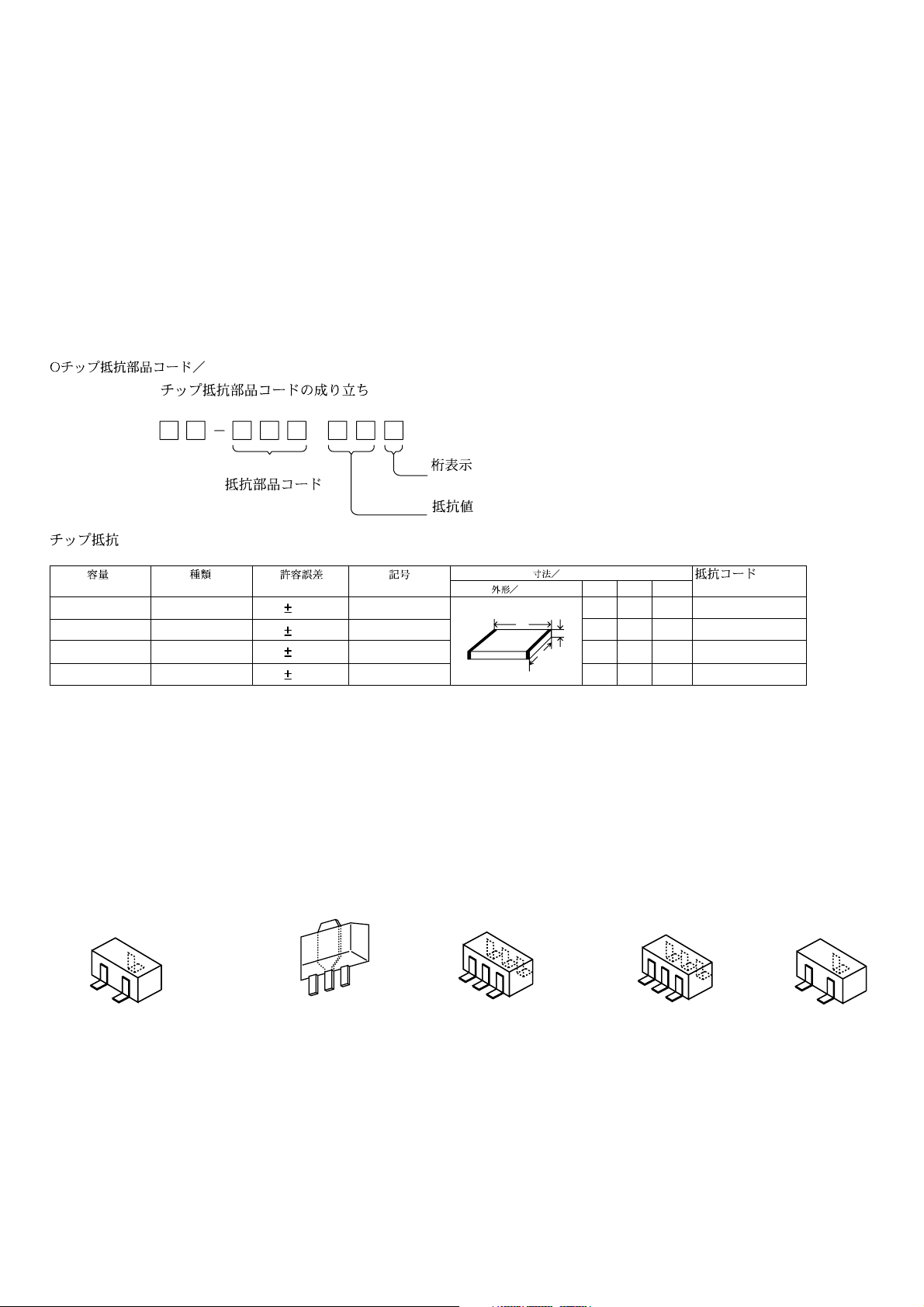
CHIP RESISTOR PART CODE
Chip Resistor Part Coding
88
REF. NO. DESCRIPTIONPART NO.KANRI
SW906 87-A91-668-080 C-SW,TACT EVQ-PQH-B55
SW907 87-A91-668-080 C-SW,TACT EVQ-PQH-B55
SW908 87-A91-668-080 C-SW,TACT EVQ-PQH-B55
SW909 87-A91-668-080 C-SW,TACT EVQ-PQH-B55
SW910 87-A91-668-080 C-SW,TACT EVQ-PQH-B55
SW911 87-A91-668-080 C-SW,TACT EVQ-PQH-B55
SW920 87-036-379-180 C-SW,SL1-1-2 SS350
TC801 87-A91-185-080 C-TRIMMER,CER 30P TZC03
X801 87-A70-259-010 VIB,XTAL 4.5MHZ CSA-309
X901 87-A70-255-080 C-VIB,4.19MHZ CSTRC0419MG03
KANRI
NO.
A
Resistor Code
Chip resistor
Wattage Type Tolerance
1/16W 1005 5% CJ
1/16W
1/10W
1/8W
1608
2125
3216
5%
5%
5%
TRANSISTOR ILLUSTRATION
Symbol
CJ
CJ
CJ
Figure
Value of resistor
Form
L
Dimensions (mm)
t
W
0.55
Resistor Code
108
118
128
LW t
1.0 0.5 0.35 104
1.6 0.8 0.45
2 1.25 0.45
3.2
1.6
: A
: A
B
E CBE
2SA1037AK
2SA1235F
2SA1362GR
2SC2412K
2SC2412K S
2SC2714
2SC3052F
CPH3106
C
CPH3206
DTA114TK
DTA114TK-TP
DTC114EK
DTC114TK
DTC123JK
2SA1369
2SB1132
2SD1664
B2
- 6 -
C2
E2
B1
UMG4N
E1
C1
E2
B2
UMH4N
IMX9
C1
C2
B1
E1
S
D
G
2SK302GR
Page 7
WIRING - 1 (MAIN: 1 / 2)
181920212223242526272829303132
17 16 15 14 13 12 11 10 9 8 7 6 5 4 3 2 1
A
B
C
D
E
F
G
H
I
J
K
L
M
N
O
P
Q
- 7 -
R
S
T
U
Page 8
WIRING - 1 (MAIN: 2 / 2)
A
B
C
D
E
F
G
H
151413121110987654321
16 17 18 19 20 21 22 23 24 25 26 27 28 29 30 31 32
I
J
K
L
M
N
O
P
Q
R
S
T
U
- 8 -
Page 9
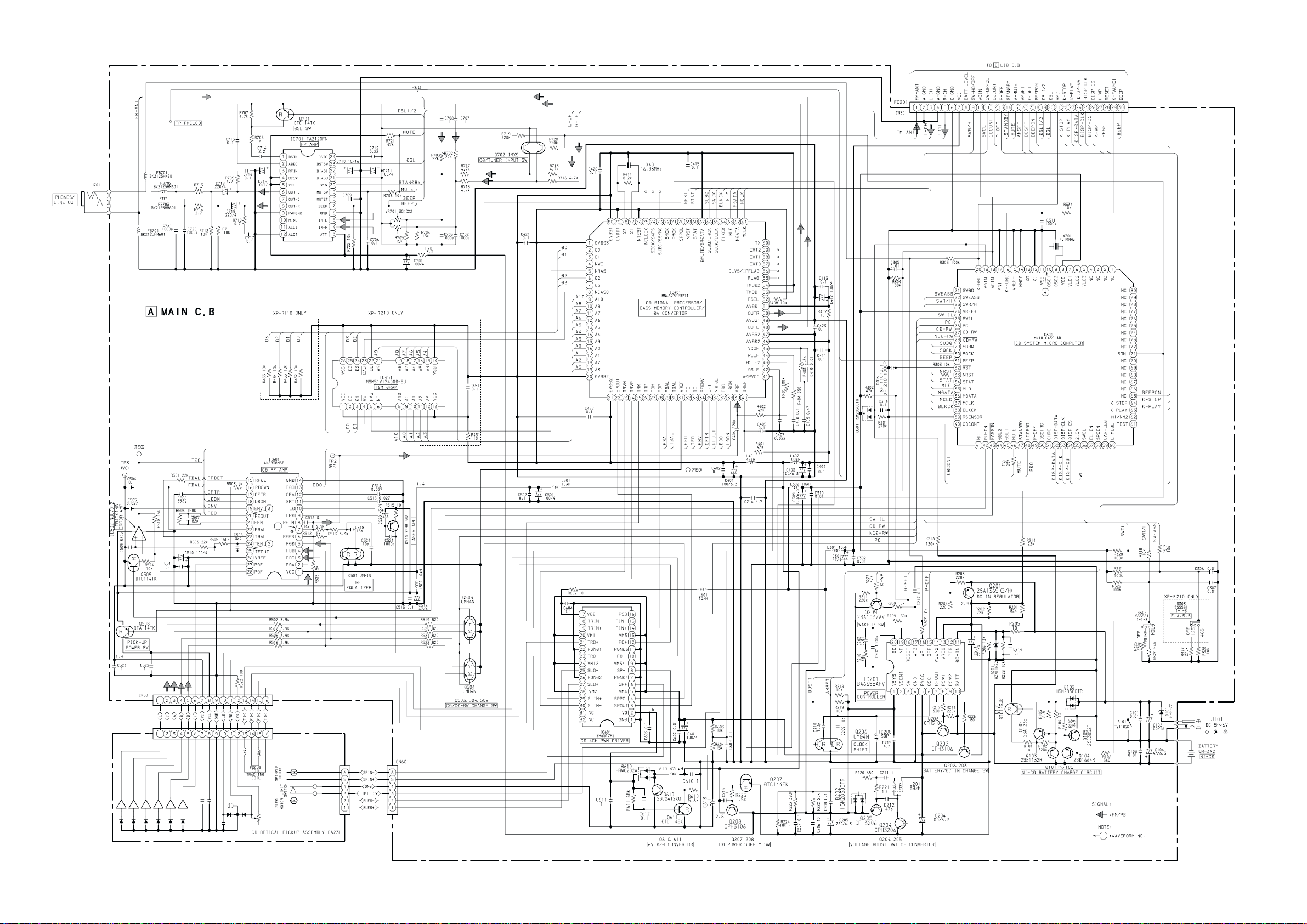
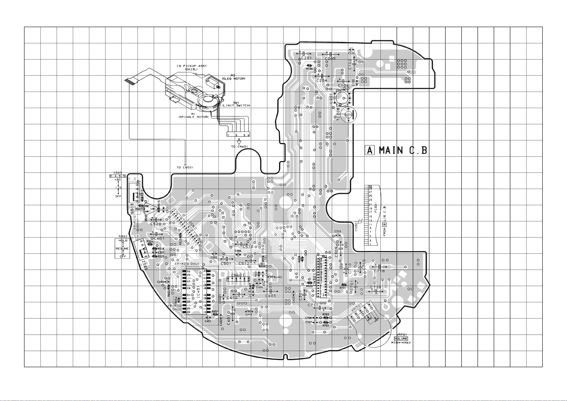
SCHEMATIC DIAGRAM - 1 (MAIN)
- 9 -
Page 10

WIRING - 2 (LID: 1 / 2)
181920212223242526272829303132
17 16 15 14 13 12 11 10 9 8 7 6 5 4 3 2 1
A
B
C
D
E
F
G
H
I
J
K
L
M
N
O
P
Q
- 10 -
R
S
T
U
Page 11

WIRING - 2 (LID: 2 / 2)
A
B
C
D
E
F
G
H
151413121110987654321
16 17 18 19 20 21 22 23 24 25 26 27 28 29 30 31 32
I
J
K
L
M
N
O
P
Q
R
S
T
U
- 11 -
Page 12

SCHEMATIC DIAGRAM - 2 (LID)
- 12 -
Page 13

IC BLOCK DIAGRAM
IC, BA6655AFV
IC, TA2120FN
IC, AN8838NSB
IC, TK11823
- 13 -
Page 14

IC, LA1827V-TLM
IC, BH6517FS
IC, LC72121V-D-TLM
- 14 -
Page 15

LCD DIAGRAM
- 15 -
Page 16

WAVEFORM
1IC501 PIN 7 (RF)
2IC501 PIN 25 (TEOUT)
0.5 V/div
0.2 µs/div
3IC501 PIN 20 (FEOUT)
50 mV/div
1 ms/div
4IC301 PIN 10 (OSC1)
50 mV/div
1 ms/div
1 V/div
50 ns/div
- 16 -
Page 17

IC,MN101C439-AB
Pin No. Pin Name I/O Description
1 ~ 4 NC - Not connected.
5 ~ 7 VLC3 ~ 1 - LCD Voltage divider resistor3 ~ 1 (Not used.)
8 VDD - Micro-computer power voltage (2.8 V).
9 OSC2 O Main clock oscillator (4.2336 MHz).
10 OSC1 I Main clock oscillator (4.2336 MHz).
11 VSS - Micro-computer GND.
12 XI I Sub clock input GND (Not used).
13 XO O Sub clock output (Not used).
14 MMOD I Memory mode switch input (Single chip mode).
15 VREF- - A/D converter GND.
16 K-FUNC I Function key input.
17 AN1 I Connected to GND.
18 AC IN I AC adaptor detection terminal.
19 VD IN I Battery voltage measuring terminal.
20 K-RMC I Wired remote control input terminal.
21 SWD0 I Digital out “ON/OFF” input (Not used).
22 SWEASS I EASS mode. SW input terminal.
23 SWR/H I RESUME/HOLD SW input terminal.
24 VREF+ - Connected to VDD.
25 SWIL I Limit SW input.
26 PC I CD servo driver power OFF output. “L” power OFF.
27 CD-RW O CD-RW PLAYBACK gain up seletion output. “H” = Gain up.
28 CD-RW O CD-RW PLAYBACK gain up seletion output. “L” = Gain up.
29 SUBQ I DSP sub-code Q input.
30 SQCK O DSP sub-code clock output.
31 BEEP O Buzzer output for headphone.
32 RST - Micro-computer reser input.
33 NRST O DSP RESET output.
34 STAT I DSP STAT input.
35 MLD O DSP MLD output.
36 MDATA O DSP MDATA output.
37 MCLK O DSP BLKCK input.
38 BLKCK I DSP BLKCK input.
39 RSENSOR I Connected to GND.
40 CDCONT I CD/Tuner mode input.
41 IRQ3 I Not connected.
42 PU-ON O H/A power down output.
43 EASSON O Gain up in EASS selection output. EASS on = “L”
44 DSL2 O Not used.
45 DSL1 O Not used.
- 17 -
Page 18

Pin No. Pin Name I/O Description
46 MUTE O Audio mute output.
47 STANDBY O Not used.
48 LCDRDO O Wired LCD remote control output.
49 P-OFF O Not used.
50 DSCHRG O Electric discharge output.
51 CHRG O Electric charge output.
52 DISP-DATA O LCD display data output.
53 DISP-CLK O LCD display data clock output.
54 DISP-CS O LCD display data chip selection output.
55 SEG25 O Not used.
56 SWCL I Cover OPEN/CLOSE detection SW input.
57 EL-ON O EL back light control output.
58 SPCON O Spindle PWM control output.
59 CAR-LED O CAR-KIT model button LED light on output, “H” = Light ON
60 E-MODE I Control spindle shaft votation (EASS only), “L” = Control spindle shaft votation mode.
61 TEST I Test input.
62 M1/NM2 O Not used.
63 K-PLAY I PLAY Key input terminal.
64 K-STOP I STOP Key input terminal.
65 BEEP-ON I BEEP ON/OFF. “H” = ON.
66 ~ 70 NC O Not connected.
71 SON O CD system power control output.
72 ~ 80 SEG8 ~ 0 O Not connected.
- 18 -
Page 19

IC,uPD789405AGK-A12-9EU
Pin No. Pin Name I/O Description
1 VDD - +3 V power supply.
2 BIAS - LCD driver power supply.
3 ~ 5 VLC0 ~ 2 - LCD driver power voltage.
6 VSS1 - GND.
7 ~ 10 COM0 ~ 3 O LCD common output.
11 ~ 27 SEG0 ~ 16 O LCD segment output.
28 ~ 30 NC - Not connected.
31 DSL1 O “H” when DSL1 output.
32 DSL2 O “H” when DSL2 output.
33 STBY O “H” when STBY output.
34 BEEP-ON O “H” output when CD BEEP is “ON”.
35 CS O E2P-ROM chip select.
36 B-FULL O “L” when “battery level LED-FULL” is illumenated.
37 B-MID O “L” when “battery level LED-MID” is illumenated.
38 B-EMP O “L” when “battery level LED-EMP” is illumenated.
39 AVDD - AD converter analogue power.
40 AVREF - AD converter reference power.
41 K-PSB I PLAY, STOP, BAND keys input.
42 K-FUNC1 I KEY input 1.
43 K-FUNC2 I KEY input 2.
44 BATT-LEVEL I BATT level input for battery level indication.
45 HOLD/OFF I “L” input when in HOLD mode.
46 REMO-IN I Remote control AD figure input.
47 TU-SEL I Japan or oversea settings input. “H” = Japan, “L” = oversea.
48 AVSS - GND for AD converter.
49 DATA-IN I E2P ROM data input.
50 DATA-OUT O E2P ROM data output.
51 DISP-CS I Chip selection input for CD indication data.
52 SK O E2P ROM clock output.
53 BEEP O BEEP output (it is fixed due to square-wave output.
54 DISP-DATA I CD detection data input.
55 NC O Not connected.
56 DISP-CLK I Clock input for CD detection data.
57 AM-STEP I AM STEP (9K/10K) switch input.
58 K-PLAY O “H” output when PLAY key is pressed.
59 K-STOP O “H” output when STOP key is pressed.
60 K-OP/CL I Cover detection. “L” input when the cover is OPEN.
61 CD-CONT O “L” output when CD is ON.
62 P-OFF O “L” output when power is off.
63 A-MUTE O MUTE output.
- 19 -
Page 20

Pin No. Pin Name I/O Description
64 AM-SFT O For “DD convertor” oscillator terminal clock shift.
65 DD-SFT O For “DD convertor” oscillator terminal clock shift.
66 CLK-SFT O “H” output when microcomputer oscillator terminal clock shift.
67 RESET I Reset input.
68 XTAL2 O Connection terminal to oscillator terminal.
69 XTAL1 I Connection terminal to oscillator terminal.
70 VSS - GND.
71 VDD - +3 V power supply.
72 XT2 - Not connected.
73 XT1 - Connected to GND.
74 VDD - Connected to VDD.
75 AC-IN I “H” input when AC adapter connected.
76 T-ON O “L” output when TUNER is ON.
77 PLL-DI I PLL data input.
78 PLL-CE O PLL chip enable.
79 PLL-CLK O PLL-CLK.
80 PLL-DO O PLL data output.
- 20 -
Page 21

IC,MN662728RPT1
Pin No. Pin Name I/O Description
1 DVDD - DRAM interface power (terminal No. 2 to 19).
2 ~ 3 D0 ~ 1 I/O DRAM data input/output signal 0 ~ 1.
4 NWE O DRAM write enable signal.
5 NRAS O DRAM RAS control signal.
6 ~ 7 D2 ~ 3 I/O DRAM data input/output signal 2 ~ 3.
8 NCAS0 O DRAM CAS control signal 0.
9 NCAS1 O
10 ~ 14 A8 ~ 4 O DRAM address signal 8 ~ 4.
15 A9 O DRAM address signal 9.
16 ~ 19 A0 ~ 3 O DRAM address signal 0 ~ 3.
20 DVSS2 I Digital circuit GND.
21 DVDD2 I Digital circuit power.
22 SPOUT O Spindle motor driver signal output.
23 TRVM O Traverse drive output (+ polar output).
24 TRVP O Traverse drive output (- polar output).
25 TRM O Tracking drive output (+ polar output).
26 TRP O Tracking drive output (- polar output).
27 FOM O Focus drive output (+ polar output).
28 FOP O Focus drive output (- polar output).
29 FBAL O Focus balance adjustment output.
30 TBAL O Tracking balance adjustment output.
31 VREF I DA output reference voltage (FBAL, TBAL, DSLF2).
32 FE I Focus error signal input (analogue input).
DRAM CAS control signal 1 ( when 1M or 4M x2 are used).
DRAM address signal 10 (when 16M DRAM is used).
33 TE I Tracking error signal input (analogue input).
34 RFENV I RF envelope signal input (analogue input).
35 OFT I Off track signal input. “H” = Off track.
36 NRFDET I RF detection signal input. “L” = Detected.
37 BDO I Drop out signal input. “H” = Drop out.
38 LDON O Laser ON signal output. “H” = ON.
39 ARF I RF signal input.
40 IREF I Reference current input terminal.
41 ADPVCC I AD reference voltage input (analogue input).
42 DSLF O DSL loop filter terminal.
43 DSLF2 O DSL unbalanced current correction.
44 PLLF O PLL loop filter terminal.
45 VCOF O Jitter free VCO loop filter terminal.
46 AVDD2 I Analogue circuit power. (for DSL, PLL, VCOF, AD, DA).
47 AVSS2 I Analogue circuit GND. (for DSL, PLL, VCOF, AD, DA).
48 OUTL O Lch audio output.
- 21 -
Page 22

Pin No. Pin Name I/O Description
49 AVSS1 I Analogue circuit GND.
50 OUTR O Rch audio output.
51 AVDD1 I Analogue circuit power.
52 FSEL I Noise filter ON/OFF switch input. “L” = ON, “H” = OFF.
53 TMOD1 I Terminal mode switch input terminal 1, Normally set to “L”.
54 TMOD2 I Terminal mode switch input terminal 2, Normally set to “L”.
55 FLAG O Flag signal output.
Command switch: Spindle servo phase synchronizing signal output.
56 CLVS/IPFLAG O “H” = CLV, “L” = Rough servo.
Interpolation flag signal output. “H” = Interpolation.
57 EXT0/ISRDATA I/O Command switch: Extension input/output port 0, SRDATA input.
58 EXT1/ILRCK I/O
59 EXT2/IBCLK I/O Command switch: Extension input/output port 2, BCLK input.
60 TX O Digital audio interface output signal.
61 MCLK I Microcomputer command clock signal input. (data is latched at loading edge.)
62 MDATA I Microcomputer command data signal input.
63 MLD I Microcomputer command load signal input. “L” = Load.
Command switch: Extension input/output port 1, LRCK input.
“H” = Lch audio data, “L” = Rch audio data.
64 BLKCK O
65 SQCK/BCLK I/O Command switch: Sub-code Q resistor external clock input, SRDATA bit clock output.
66 SUBQ/LRCK O
67 DMUTE/SRDATA I/O Command switch: Muting input, “H” = MUTE. Serial data output.
68 STAT O NTLOCK, BSSEL, SUBQ DATA, CDTEXT DATA, SHOCK RESISTANCE READ
69 NRST I Reset input “L” = Reset.
70 SPPOL O Spindle motor drive signal output. (polar output)
71 PMCK O 88.2 KHz clock signal output.
72 SMCK O 4.2336 MHz clock signal output.
73 SUBC/SSYNC O Command switch: Sub-code serial output, Sector SYNC output.
74 SBCK/64FS I Command switch: Clock input for sub-code serial output, 64FS output.
75 NCLDCK O Sub-code frame clock signal output. (fCLDCK = 7.35 KHz)
76 NTEST I Test terminal normally set to “H”.
77 X1 I Quartz oscillator circuit input terminal f = 16.9344 MHz.
Sub-code block clock signal fBLKCK = 75 Hz. (in normal PLAY mode)
/CDTEXT SYNC signal (fDQSY = 300 Hz. (in normal PLAY mode)
Command switch: Sub-code Q data output, L, R discrimination signal output.
“H” = Lch audio data, “L” = Rch audio data.
Status signal (CRC, RESY, CLVS, NTTSTOP, SQOK, FLAG6, SENSE,NFLOCK
DATA.
78 X2 O Quartz oscillator circuit output terminal f = 16.9344 MHz.
79 DVDD1 I Digital circuit power.
80 DVSS1 I Digital circuit GND.
- 22 -
Page 23

CN501
IC451
CN601
CN301
VR701
TC208
S101
OPEN/CLOSE SW LAND
PHONES/LINE OUT
J701
1
3
6
CD TEST MODE
1
A
MAIN C.B
PHONES/LINE OUT
Q204
c
TEST LAND
IC301
(TEO)
TP3
(VC)
(FEO)
GND
TP2(RF)
IC501
J701
3
6
(another side)
IC401
The servo circuit of this model is designed to be adjustment-free and the adjustment value and disc distinction (CA-DA. CD-R and CD-RW etc.) is
adjusted by within the IC. Therefore the adjustment is performed by each TOC reading. The adjustment conditions within the IC of each servo can be
monitored in this test mode.
1. How to start the Test Mode
GND
Starting method of the test mode differ depending upon the type of disc being used. This is because the adjustment values of each servo also
differ depending upon the type of disc.
When using the CD-DA or CD-R
1) Short-circuit the test land and the OPEN/CLOSE SW land.
2) Insert the AC plug and install the CD-DA or CD-R disc.
3) Press the PLAY and STOP buttons in this sequence and read the TOC.
4) Press the DISPLAY/ENTER button and confirm that all LCD light up.
IC901
LCD901
FM-ANT
BPF801
When using the CD-RW
2
TP1(VT)
L802
IFT803
L801
4
1) Short-circuit the test land and the OPEN/CLOSE SW land.
2) Insert the AC plug and install the CD-RW disc.
3) Press the PLAY, STOP and DSL buttons in this sequence and read the TOC. The LCD display should display CD-r at this point.
4) Press the DISPLAY/ENTER button and confirm that all LCD light up.
Note 1) If the TOC cannot be read, press the DISPLAY/ENTER button once “Err” has appeared on the LCD, causing all the LCDs to become lit
up. The following steps 2 and 3 can be confirmed even if the TOC cannot be read.
Note 2) By repeatedly pressing the DISPLAY/ENTER button, all LCD will light up and the TOC display will be repeated.
Note 3) By repeatedly pressing the DSL button, the “CD-d” and “CD-r” displays will be repeated.
When the LCD displays “CD-d,” ’ CD-DA, CD-R is selected.
ANT801(BAR ANTENNA)
TC801
3
Note 4) The test mode is cancelled by disconnecting the AC plug and removing the soldering of short land.
3
2. DISC distinction (confirmation of FE waveform)
This mode is possible to perform a confirmation of the disc distinction.
When the LCD displays “CD-r,” ’ CD-RW is selected.
Confirmation method
1) Press the DSL button and select “CD-d” or “CD-r” (Refer to Note 3).
2) Install the disc.
3) Press the MODE button.
- 23 -
Page 24

The LCD will change as follows.
Example: Test disc: TCD-782, DISC type select: CD-d, Judgement value: 7F, Measurement value: 3D BE.
Judgement value Measurement value
*All numerical values are displayed in HEX
switchover sequence is as stated below.
Confirmation mode OFF -> Focus bias (FB) -> Tracking balance (TB) -> Tracking gain (TG) -> Tracking error offset (TEO) -> Focus gain (FG)
-> Focus error offset (FEO) -> Confirmation mode OFF
Example: Tracking error offset (TEO) Adjustment value: 03
What disc the IC has selected can be understood according to this judgment value.
The decision standard of IC is as follow.
LCD displays “CD-d” LCD displays “CD-r”
0 < Judgment value < 10 No disc No disc
10 < Judgment value < 32 CD-RW No disc
32 < Judgment value < C8 CD-DA and CD-R CD-RW
C8 < Judgment value CD-DA and CD-R
The state of the FE waveform can also be understood from this judgment value.
3. Confirmation of sled movement
By pressing the F. SKIP or B. SKIP button continuously when all LCD light up, it is possible to transfer the pick-up to either the outer circumference or the inner circumference (the LCD is to remain all light up).
4. Confirmation of the RF level
Test point: RF and VC (Vref)
Test disc: TCD-782
Confirm that the RF waveform appears as shown below.
At 0.8Vp-p or greater
VOLT/DIV: 200mV
TIME/DIV: 0.5us
5. Confirmation of tracking balance
Test point: TE and VC (Vref)
Test disc: TCD-782
Press the DSL button while the test disc is playing and confirm that the traverse waveform is as is shown below.
VC
Tracking error offset (TEO) display Adjustment value
*Adjustment values are displayed in HEX.
ADJUSTMENT
< TUNER SECTION >
1. DD converter clock adjustment
Settings : • Test point : Q204 Collector
• Ajustment location: TC208
Method : Set to AM603 kHz and adjust TC208 so that
the test point becomes 360kHz.
2. AM VT Check
Settings : • Test point : TP1 (VT)
Method : Set to AM 530kHz(AU,ALH), 531kHz(Other)
and check that the test point is 1.0V ± 0.5V and
set to AM 1710kHz(AU,ALH), 1602kHz(Other)
and check the test point is 7.5V ± 1.0V(AU,ALH),
6.5V ± 1.0V (Other).
3. AM Tracking Adjustment
Settings : • Test point : HP OUT (VOLUME MAX)
• Adjustment location :
BAR ANTENA................................600kHz(AU,ALH)
BAR ANTENA................................603kHz(Other)
TC801..............................................1400kHz(AU,ALH)
TC801..............................................1404kHz(Other)
* Repeat this adjustment a few times until the wave
shape has the maximum amplitude.
4. AM IF Adjustment
IFT803.........................................999kHz(Other)
IFT803.......................................1404kHz(AU,ALH)
5. FM VT Adjustment(Lower side)
Settings : • Test point : TP(VT)
• Adjustment location : L801
Method : Set to FM 87.5MHz and adjust L851 so that the test
point becomes 1.5 ~ 2.0V.
6. FM Tracking Adjustment
Settings : • Test point : HPOUT (VOLUME MAX)
• Adjustment location :
L802................................................87.5MHz
* Repeat this adjustment a few times until the distortion
is minimum.
VOLT/DIV: 200mV
TIME/DIV: 2ms
6. Confirmation of each servo
It is possible to confirm the adjustment value of each servo by repeatedly pressing the MODE button while the test disc is playing. The
- 24 -
Page 25

MECHANICAL EXPLODED VIEW 1 / 1
2
12
4
1
3
78
5
6
LCD
9
13
17
18
19
15
16
11
20
DA23L
21
22
14
P.C.B
P.C.B
5
A
A
26
25
27
24
23
LID,BATT
B
B
- 25 -
Page 26

MECHANICAL PARTS LIST 1 / 1
REF. NO. DESCRIPTIONPART NO.
NO.
1 8A-HC1-006-010 PANEL,DISPLAY
2 8A-HC1-005-010 PANEL,LID CD
3 8A-HC1-007-010 WINDOW,DISPLAY
4 8A-HC1-001-010 LID,CD<R210>
4 8A-HCB-001-010 LID,CD(11)<R110>
5 8A-HC1-201-010 SPR-T,OPEN
6 85-HC6-205-110 SHAFT,LID(300) HK
7 8Z-HC1-610-010 ANT,BAR-ANTENNA
8 8A-HC1-207-010 PLATE,LCD
9 8Z-HC1-209-010 JOINT,LCD ZHC-1
10 8A-HC1-009-010 HLDR,LID CD
11 8A-HC1-015-010 LENS,LED
12 8A-HC1-008-010 KEY,PLAY
13 8A-HC1-014-010 KEY,BAND
14 8A-HC7-018-010 LEVER,OPEN
15 8A-HC1-002-010 CABI,CENTER<R210>
15 8A-HCB-002-010 CABI,CENTER(11)<R110>
16 8A-HC1-203-010 LEVER,OPEN
17 8A-HC1-010-010 KNOB,SL OPEN
18 8A-HC1-202-010 SPR-T,KNOB
REF. NO. DESCRIPTIONPART NO.KANRI
19 8A-HC1-204-010 HLDR,OPEN
20 8Z-HC1-225-010 DMPR,MECHA(SP)
21 8A-HC1-206-010 BAT-CONTACT,(-)
22 8A-HC1-205-010 BAT-CONTACT,(+)
23 8Z-HC7-216-010 BAT-CONTACT,(+)(-) (SP)
24 8A-HC1-013-010 KNOB,SL EASS<R210>
25 8A-HC1-011-010 KNOB,SL HOLD
26 8A-HC1-012-010 CABI ASSY,BOTTOM<R210>
26 8A-HCB-005-010 CABI ASSY,BOTTOM(11)<R110>
27 8Z-HC4-027-010 FOOT,DIA10
A 87-067-384-010 SCREWVT1.4-3.5HL
B 87-067-869-010 V+1.7-8 HL BLK
KANRI
NO.
COLOR NAME TABLE
Basic color symbol Color Basic color symbol Color Basic color symbol Color
B Black C Cream D Orange
G Green H Gray L Blue
LT Transparent Blue N Gold P Pink
R Red S Silver ST Titan Silver
T Brown V Violet W White
WT Transparent White Y Yellow YT Transparent Yellow
LM Metallic Blue LL Light Blue GT Transparent Green
LD Dark Blue DT Transparent Orange
- 26 -
Page 27

CD MECHANISM EXPLODED VIEW 1 / 1
D
D
2
4
9
8
6
A
3
5
1
7
C
10
B
CD MECHANISM PARTS LIST 1 / 1
REF. NO. DESCRIPTIONPART NO.
1 S0-A41-A20-600 PICKUP LASER ASSY
2 SM-10A-108-001 MOTOR ASSY SPINDLE
3 S0-M10-A10-900 MOTOR SLED ASSY
4 S2-311-A12-200 CHASSIS
5 S2-511-A23-200 GEAR MIDDLE
6 S2-511-A23-100 GEAR,SCREW
7 S2-511-A23-400 GEAR,RACK
8 S2-511-A07-900 SPINDLE SCREW
9 S4-S13-A00-200 SW,LEAF
10 S2-451-A18-100 HOLDER GEAR
A SS-EXE-A04-000 SCR PAN PCS 1.4-2.2
B SS-GXE-A00-300 SPECIAL SCREW
C SS-EXE-A14-100 SPECIAL SCREW
D SS-GXE-A00-202 SPECIAL SCREW M1.7-4.0
KANRI
NO.
- 27 -
Page 28

2–11, IKENOHATA 1–CHOME, TAITO-KU, TOKYO 110, JAPAN TEL:03 (3827) 3111
Printed in Singapore9820572 0251431
 Loading...