

Page 1
SS-US301/SW-US301/UZ-US301
Power requirements and others
Power source
U.S.A. model: 120 V AC, 60 Hz
Other models: 220 - 240 V AC, 50/60 Hz
Power consumptions
U.S.A. model: 60 W
1 W (at the Power Saving
Mode)
Other models: 60 W
0.5 W (at the Power
Saving Mode)
Supplied accessories
USB cable (1.8 m (5.9 ft.) ) (1)
Design and specifications are subject to change without
notice.
SERVICE MANUAL
Ver 1.0 2003.12
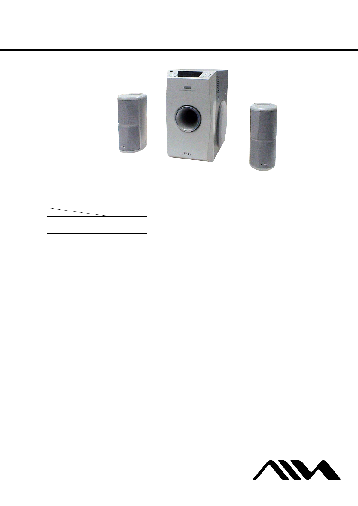
SS-US301 SW-US301 SS-US301
• UZ-US301 consists of the following models respectively.
UZ-US301
Subwoofer SW-US301
Satellite Speaker SS-US301
US Model
AEP Model
UK Model
E Model
For the U.S.A. model
AUDIO POWER SPECIFICATIONS
POWER OUTPUT AND TOTAL HARMONIC
DISTORTION:
With 4 ohms loads subwoofer driven, from 20 - 200 Hz;
rated 20 watts minimum RMS power, with no more than
0.8% total harmonic distortion from 250 milliwatts to
rated output.
UZ-US301
SW-US301 (Subwoofer)
Type Active subwoofer, bass
Figure 130 mm (5
Maximum output power 45 W
Rated impedance 4 ohms
Dimensions (w/ h/d) 160 × 300 × 300 mm
Mass 5.8 kg (12.79 lb)
* Magnetically shielded type
9-961-437-01 Sony Corporation
2003L05-1 Aiwa Original Products
C 2003.12 Published by Sony Engineering Corporation
reflex
type*
30 W (10 % THD)
(6
in.) (not including the
projecting parts)
3
/8 × 11 7/
1
/8 in.), cone
× 11 7/
8
SPECIFICATIONS
Inputs and Outputs
USB Type B
LINE LINE IN (pin jack)
Speaker speaker output
SS-US301 (Satellite Speaker)
Type · Figure Front 58 mm (2 3/8 in.),
Maximum output power
Front 25 W × 2
Dual Center 25 W
Rated impedance Front 8 ohms
8
Dimensions (w/ h/d) 85 × 200 × 125 mm
Mass Approx. 650 g (1.43 lb) ×
* Magnetically shielded type
(terminal)
cone type*, closed type
Dual Center 48 mm
15
(1
/
uni directional type
17 W × 2 (10 % THD)
17 W (10 % THD)
Dual Center 4 ohms + 4
ohms
3
(3
/
8
(not including the
projecting parts)
2
in.), cone type*
16
7
× 7
/8 × 5 in.)
USB ACTIVE SPEAKER SYSTEM
Page 2
SS-US301/SW-US301/UZ-US301
r
Notes on chip component replacement
•Never reuse a disconnected chip component.
• Notice that the minus side of a tantalum capacitor may be damaged by heat.
SAFETY CHECK-OUT
After correcting the original service problem, perform the following safety check before releasing the set to the customer:
Check the antenna terminals, metal trim, “metallized” knobs,
screws, and all other exposed metal parts for AC leakage.
Check leakage as described below.
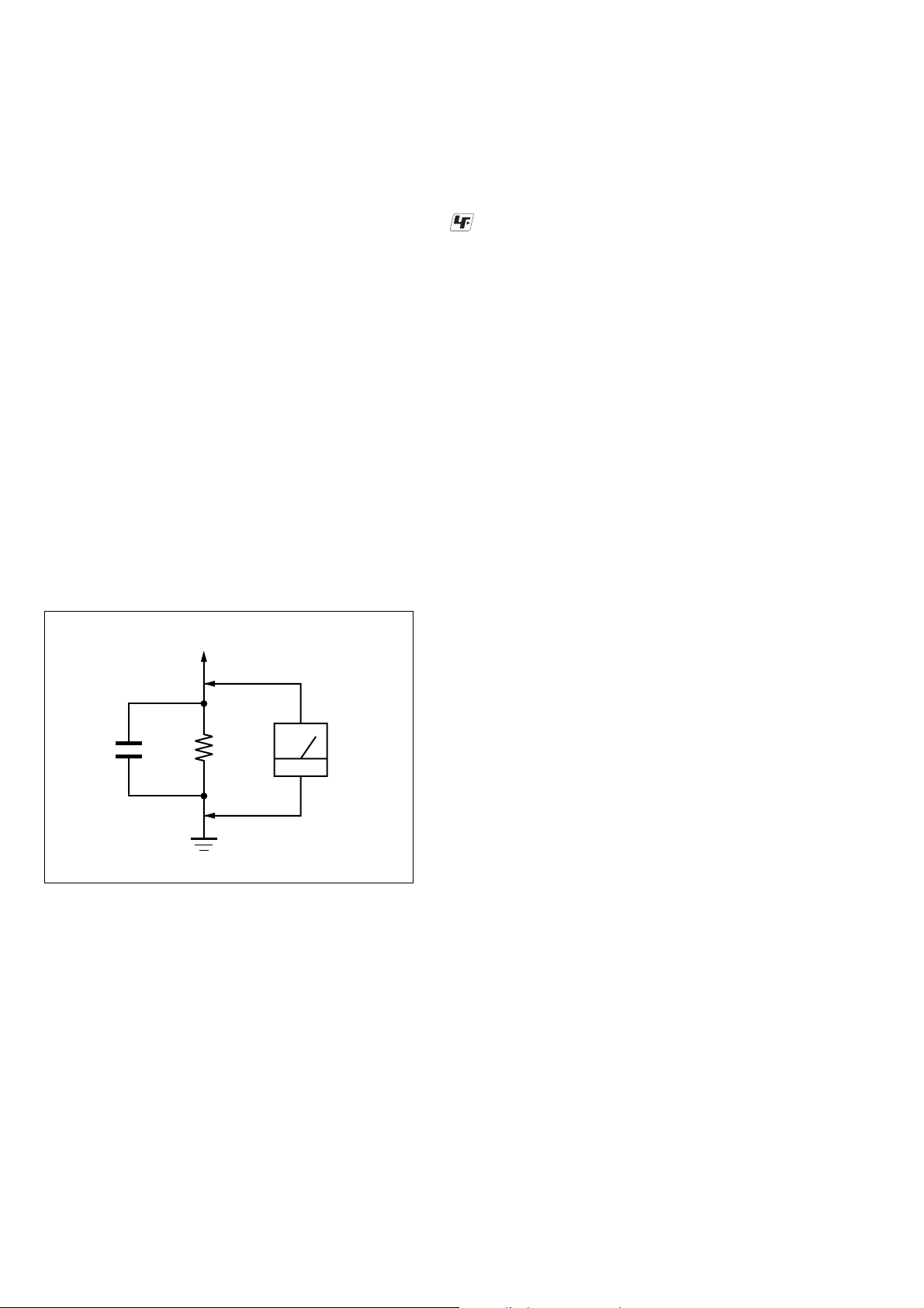
LEAKAGE TEST
The AC leakage from any exposed metal part to earth ground and
from all exposed metal parts to any exposed metal part having a
return to chassis, must not exceed 0.5 mA (500 microamperes.).
Leakage current can be measured by any one of three methods.
1. A commercial leakage tester, such as the Simpson 229 or RCA
WT -540A. Follo w the manufacturers’ instructions to use these
instruments.
2. A battery-operated AC milliammeter. The Data Precision 245
digital multimeter is suitable for this job.
3. Measuring the voltage drop across a resistor by means of a
VOM or battery-operated AC voltmeter. The “limit” indication is 0.75 V, so analog meters must have an accurate lowvoltage scale. The Simpson 250 and Sanwa SH-63Trd are e xamples of a passive VOM that is suitable. Nearly all battery
operated digital multimeters that have a 2 V A C range are suitable. (See Fig. A)
UNLEADED SOLDER
Boards requiring use of unleaded solder are printed with the leadfree mark (LF) indicating the solder contains no lead.
(Caution: Some printed circuit boards may not come printed with
the lead free mark due to their particular size)
: LEAD FREE MARK
Unleaded solder has the following characteristics.
• Unleaded solder melts at a temperature about 40 ˚C higher than
ordinary solder.
Ordinary soldering irons can be used but the iron tip has to be
applied to the solder joint for a slightly longer time.
Soldering irons using a temperature regulator should be set to
about 350 ˚C.
Caution: The printed pattern (copper foil) may peel away if the
heated tip is applied for too long, so be careful!
• Strong viscosity
Unleaded solder is more viscou-s (sticky, less prone to flow)
than ordinary solder so use caution not to let solder bridges occur such as on IC pins, etc.
• Usable with ordinary solder
It is best to use only unleaded solder but unleaded solder may
also be added to ordinary solder.
To Exposed Metal
Parts on Set
AC
1.5 k
0.15 µF
Fig. A. Using an AC voltmeter to check AC leakage.
Ω
Earth Ground
voltmete
(0.75 V)
SAFETY-RELATED COMPONENT WARNING!!
COMPONENTS IDENTIFIED BY MARK 0 OR DOTTED
LINE WITH MARK 0 ON THE SCHEMATIC DIAGRAMS
AND IN THE PARTS LIST ARE CRITICAL TO SAFE
OPERATION. REPLACE THESE COMPONENTS WITH
SONY PARTS WHOSE PART NUMBERS APPEAR AS
SHOWN IN THIS MANU AL OR IN SUPPLEMENTS PUBLISHED BY SONY.
2
Page 3

TABLE OF CONTENTS
1. SERVICING NOTE................................................. 4
2. GENERAL .................................................................. 5
3. DISASSEMBLY
3-1. Disassembly Flow ........................................................... 6
3-2. Top Chassis ..................................................................... 6
3-3. MAIN Board ................................................................... 7
3-4. Front Cabinet Section ..................................................... 7
4. TEST MODE............................................................. 8
5. DIAGRAMS
5-1. Block Diagram ................................................................ 9
5-2. Note for Printed Wiring Boards and
Schematic Diagrams ....................................................... 10
5-3. Printed Wiring Board – MAIN Board – ........................ 12
5-4. Schematic Diagram – MAIN Board (1/3) – .................. 13
5-5. Schematic Diagram – MAIN Board (2/3) – .................. 14
5-6. Schematic Diagram – MAIN Board (3/3) – .................. 15
5-7. Printed Wiring Board – DISPLAY Board – .................. 16
5-8. Schematic Diagr am – DISPLAY Board – ..................... 17
5-9. Printed Wiring Board – AMP Board (US model) – ...... 18
5-10. Schematic Diagram – AMP Board (US model) – ......... 19
5-11. Printed Wiring Board
– AMP Board (Except US model) – ............................... 20
5-12. Schematic Diagram
– AMP Board (Except US model) – ............................... 21
5-13. Printed Wiring Board
– SUB Board (Except US model) –................................ 22
5-14. Schematic Diagram
– SUB Board (Except US model) –................................ 22
SS-US301/SW-US301/UZ-US301
6. EXPLODED VIEWS
6-1. Overall Section ................................................................ 25
6-2. Front Cabinet Section ..................................................... 26
6-3. Main Section ................................................................... 27
6-4. Rear Chassis Section ....................................................... 28
6-5. SS-US301 (L)/(R) ........................................................... 29
7. ELECTRICAL PARTS LIST .............................. 30
3
Page 4
SS-US301/SW-US301/UZ-US301
• MODEL IDENTIFICATION
– Rear View –
AUDIO I N
R
L
USB
FRONT
AUTO
POWER
ON
CENTER
OFF
PART No.
SECTION 1
SERVICING NOTE
MODEL PART No.
AEP and UK models 4-253-567-0
US model 4-253-649-0
Korean model 4-254-404-0
Singapore model 4-254-406-0
Hong Kong model 4-254-408-0
[]
[]
[]
[]
[]
4
Page 5
Location of controls
SECTION 2
GENERAL
SS-US301/SW-US301/UZ-US301
This section is extracted from
instruction manual.
^/1 (POWER) indicator
USB indicator
PHONES
^/1 (POWER)
SURROUND MODE
USB
WOOFER
LEVEL
VOLUME
USB/AUDIO IN
VOLUME LEVEL
-
6
1
USB/AUDIO IN
Connection
MD player
CD player
Game devices,
etc.
B
Audio connecting cord (not supplied)
To LINE OUT/ the
Headphones jack,
etc.
-
42-
1
2
2
304+25+46
+6 dB
7
WOOFER
S-MODE
VOLUME +/–
AUDIO IN
VOLUME
PHONES
USB
USB/AUDIO IN
Headphone jack
AUDIO IN
R
USB
AUTO
POWER
ON
CENTER
OFF
S-MODE indicator
SURROUND MODE
WOOFER
LEVEL
-
6
-
42-
VOLUME
1
Subwoofer lebel
L
FRONT
12
2
304
+2
+6 dB
5+46
7
S-MODE
To wall outlet
WOOFER
S-MODE
Woofer
VOLUME
A
To USB port
Center (R)
Front (R)
Satellite
speaker (R)
USB cable (supplied)
R
L
USB
FRONT
AUTO
POWER
ON
CENTER
OFF
Speaker cords
Hole for attaching the floor
stand (not supplied)
To USB port
RL
Red
PurpleGreen White
To your computer
Subwoofer (this system)
Speaker cords
Center (L)
Front (L)
Hole for attaching the floor
stand (not supplied)
Satellite
speaker (L)
5
Page 6
SS-US301/SW-US301/UZ-US301
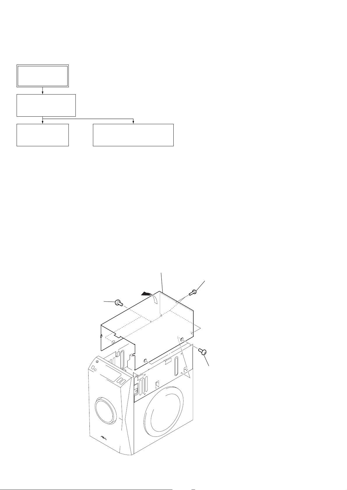
• This set can be disassembled in the order shown below.
3-1. DISASSEMBLY FLOW
Set
3-2. TOP CHASSIS
(Page 6)
SECTION 3
DISASSEMBLY
3-3. MAIN BOARD
(Page 7)
Note: Follow the disassembly procedure in the numerical order given.
3-4. FRONT CABINET SECTION
(Page 7)
3-2. TOP CHASSIS
4
top chassis
3
three screws
(BVTP3
×
10)
2
two case screws
1
two case screws
6
Page 7
SS-US301/SW-US301/UZ-US301
)
6
Insert a flat-tip screwdriver into a recess
in the bottom of the set
to raise the front cabinet section a little.
7
Insert the jig
(J-2051-238-A)
into a space made by
inserting the screwdriver,
and raise the front cabinet
section gradually.
8
front cabinet section
boss
boss
boss
1
wire (flat type) (23 core)
(CN801)
2
screw
(BVTP3
×
8)
5
screw
(BVTP3
×
8)
4
screw
(BVTP3
×
8)
3
harnness
Note : Take care not to damage the set by applying an excessive force.
3-3. MAIN BOARD
1
wire (flat type)
(23 core) (CN801)
9
main board
4
connector
(CN301)
5
connector
(CN302)
2
screw
(BVTP3
3
harness
×
8)
7
screw
8
screw
(BVTP3
×
8)
6
(BVTP3
screw
(BVTT3
×
10
×
8)
3-4. FRONT CABINET SECTION
7
Page 8

SS-US301/SW-US301/UZ-US301
SECTION 4
TEST MODE
[TEST MODE]
Procedure:
1. While pressing the [S-MODE] button and the I/1 button,
change over the [AUTO POWER] switch from OFF to ON.
2. All LED’s light up when the test mode is activated.
3. Press the [S-MODE] button to display the version. (The
corresponding [VOLUME] LED will blink. (indicated in binary
notation))
4. Press the [VOLUME +] button to increase the volume point, or
the [VOLUME
5. Press the [WOOFER] button and the woofer le v el becomes
settable, and then press the [VOLUME +] button to increase
the woofer level by 2 dB (up to +6 dB), or press the [VOLUME
-
] button to reduce the woofer lev el by 2 dB (do wn to –6 dB).
(LED display will shift one step each time the button is pressed)
Also, if the button is not pressed for 3 seconds, the volume
indication comes back.
6. Other buttons execute their functions respectively. (For the
APC (auto power control), the mode transits to APC mode
unless the button is pressed for 5 seconds)
7. Press the I/1 button to turn it OFF, and the test mode is
deactivated.
8. All settings become default values when the test mode is
deactivated.
-
] button to decrease the volume point.
8
Page 9
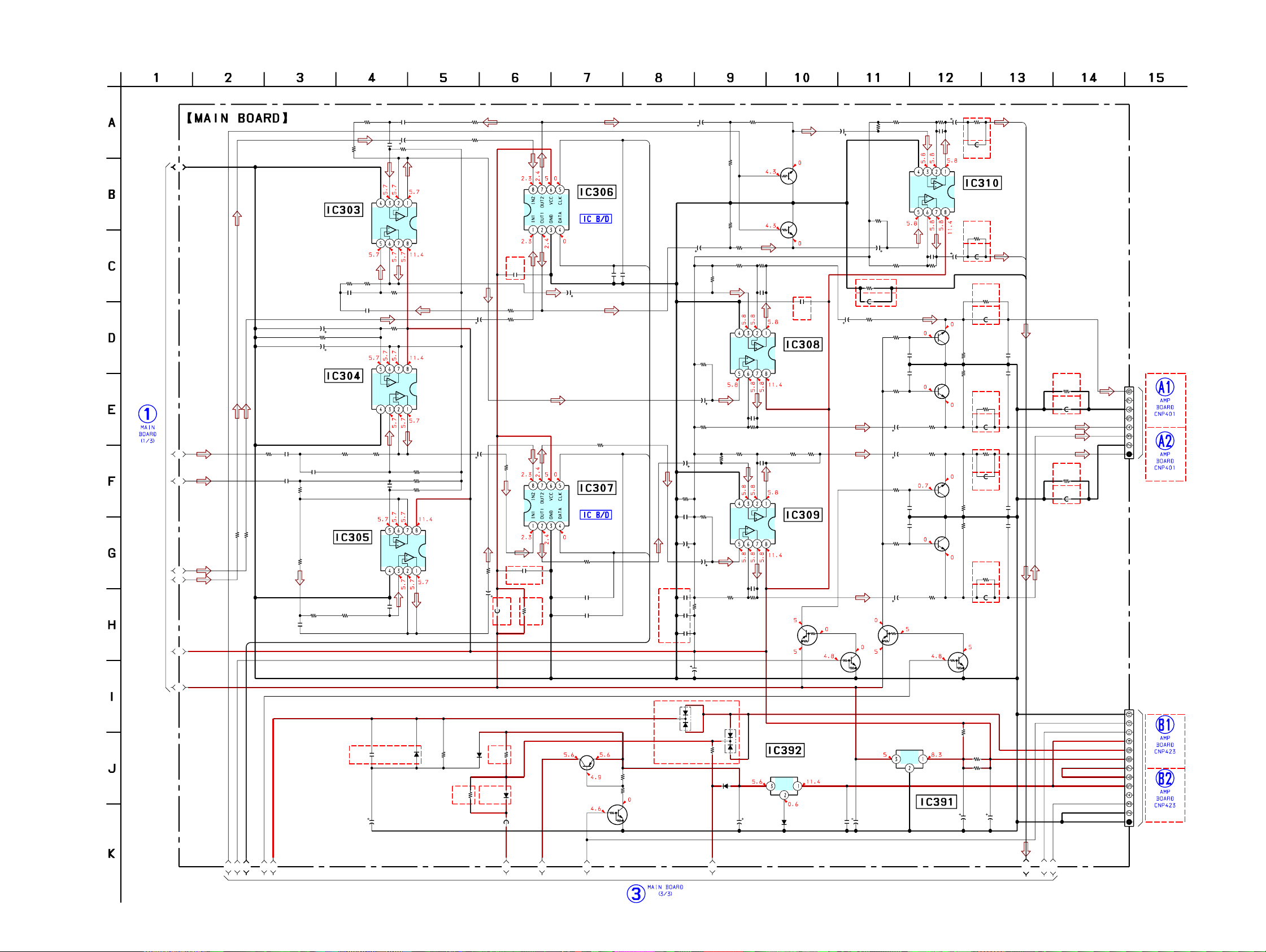
5-1. BLOCK DIAGRAM
J301
AUDIO IN
L
R-CHR
J501
2
D+
3
D–
USB
VBUS
4
USB CONTROL
SWITCH
Q501, 502
R-ch is omitted due to same as L-ch.
SIGNAL PATH
: AUDIO
: USB
CONVERTER
9
D+
8 D–
HOST28XTI1XTO
21
USB D/A
IC501
12MHz
VOUTL
VOUTR
X501
SS-US301/SW-US301/UZ-US301
SECTION 5
DIAGRAMS
MUTING
Q752
Q309
CONTROL SWITCH
+3.3V
IC502
+5.6V
IC392
RESET
SWITCH
Q801
R-CH
MUTING
Q310
MUTING
Q305, 306
IC903
MUTING
Q308
MAIN POWER
TRANSFORMER
RECT
D909
RECT
D911
RECT
D914
CONTROL SWITCH
(US)
D804
D806
T901
(EXCEPT US)
SWITCHING
POWER ON/OFF
Q902, 906
RESET SIGNAL
GENETATOR
µCOM +5V
HEADPHONE
AMP
IC310
MUTING
DATA5CLK
CLK2
+5V
IC391
B+ SWITCH
Q391, 392
M
Q303
2OUT1
7OUT2
D394
+10V
REGULATOR
Q453
+3.3V
READY
+10V
DIG +10V
PRE AMP
IC308
PRE AMP
IC309
CONTROL SWITCH
B+ SWITCH
Q451, 452
B+ SWITCH
Q904, 905
MUTING
MUTING
Q312, 313
REGULATOR
B+ SWITCH
Q909, 910
REGULATOR
1
H/P-MUTE
V-1 – V-4
V-5 – V-7
41X140
8.38MHz
H/P-S/W
X801
ELECTRICAL VOLUME
IC306
8 IN2
DATA5CLK
4
CLK1
DATA1
HIGH-PASS
FILTER
IC304
LOW-PASS
FILTER
IC305
DATA2
49VOL2-DATA
CLK2
50VOL2-CLK
59C-MUTE
51LINE-MUTE
48AMP-MUTE
46P-CON
47READY-H
36
RESET
43STOP
X2
7OUT2
HIGH-PASS
MUTING
CONTROL SWITCH
Q301
ELECTRICAL VOLUME
1 IN1
8 IN2
+5V
LED B+
LED B+
POWER AMP
FILTER
IC303
IC307
4
DATA2
REGULATOR
FAN902
(FAN)
(IC401) B+
3D SOUND PROCESSOR
IC302
5
INPUT SELECTOR
IC301
8 9
6
Q802
R-CH
USB AMP
IC506
KEY1
27
26
S701 – 706
14
15
INT
44
KEY ACTIVE
SWITCH
KEY2
1011
12
INPUT SELECTOR
CONTROL SWITCH
APC-ON/OFF
58
S801
AUTO
POWER
OFF
ON
SURROUND MODE
Q508
LINE AMP
+
(POWER ON (GRN))
(STANDBY (RED))
Q506
INPUT SELECTOR
CONTROL SWITCH
Q304
55
USB-H
D702
USB
D703 – D706
D707 – D709
D711
1
2
D712
D507
BUFFER
IC505
+
33
D701
AUDIO-DET
LIN 17LOUT
SDA12SCL16STRB
13
R-CH
+
D506
R-CH
D509
56 57 54 2
S-DATA
SYSTEM CONTROLLER
IC801
LED DRIVE
Q710
LED DRIVE
Q701
LED DRIVE
Q702
LED DRIVE
Q707 – Q709
LED DRIVE
Q711
LED DRIVE
Q712
S-CLK
S-TRB
6COUT
CLK1
DATA1
53
54
VOL1-CLK
VOL1-DATA
5
16
15
14 – 11
8 – 6
4
3
GRN-LED
RED-LED
USB-LED
S-LOW
S-HIGH
J701
PHONES
POWER AMP
IC401
(US) (EXCEPT US)
MUTE
4
22
+20V
Q901
(EXCEPT US)
5
3
9
7
17
19
21
23
ST-BY
RECT
D902
ISOLATOR
PC901
(US)
(EXCEPT US)
D393
D397
12
11R-CH
15
14
TH901
D906 D907
REGULATOR
(US)
IC902
(US)
IC802
D452
D451
D453
D454
LINE FILTER
LF901, 902
D905
+5.6V
REGULATOR
IC991
+
L
–
+
R
–
+
L
–
+
R
–
(SUB WOOFER)
F901
(US)
(EXCEPT US)
3
D
4
VCC
1
FB/OCP
POWER CONTROL
IC901
RELAY DRIVE
Q991
RELAY DRIVE
Q992
D992 – 995
RECT
FRONT
CENTER
SP101
J404
SPEAKER
(US)
RY991
RY992
T902
SUB POWER
TRANSFORMER
TO SATELLITE
SPEAKER (L)/(R)
(SS-US301)
(AC IN)
99
Page 10
SS-US301/SW-US301/UZ-US301
5-2. NOTE FOR PRINTED WIRING BOARDS AND SCHEMATIC DIAGRAMS
Note on Printed Wiring Boards:
• X : parts extracted from the component side.
• Y : parts extracted from the conductor side.
f
•
• : Pattern from the side which enables seeing.
(The other layers' patterns are not indicated.)
Caution:
Pattern face side: Parts on the pattern face side seen from
(Conductor Side) the pattern face are indicated.
Parts face side: Parts on the par ts face side seen from
(Component Side) the parts face are indicated.
• Indication of transistor.
: internal component.
C
Q
B
E
B
These are omitted.
Q
CE
These are omitted.
Note on Schematic Diagram:
• All capacitors are in µF unless otherwise noted. pF: µµF
50 WV or less are not indicated except for electrolytics
and tantalums.
• All resistors are in Ω and 1/
specified.
f
•
• 2 : nonflammable resistor.
• C : panel designation.
Note: The components identified by mark 0 or dotted line
• A : B+ Line.
•Voltages and waveforms are dc with respect to ground
•Voltages are taken with a V OM (Input impedance 10 MΩ).
•Waveforms are taken with a oscilloscope.
• Circled numbers refer to waveforms.
• Signal path.
: internal component.
with mark 0 are critical for safety.
Replace only with part number specified.
under no-signal conditions.
no mark : AUDIO
(): USB
Voltage variations may be noted due to normal production tolerances.
Voltage variations may be noted due to normal production tolerances.
F : AUDIO
N : USB
4
W or less unless otherwise
•Waveform
– MAIN Board –
1 IC801 r; (X2)
4 Vp-p
119 ns
1010
Page 11

• IC Block Diagrams
– MAIN Board –
IC302 QS7779CM-G-E2
SS-US301/SW-US301/UZ-US301
IC501 PCM2704DBR
QXAC3
QXAC2
QXAC1
RIN
LIN
COUT
CIN
VREFIN
VREFOUT
VREF
GND
SPRD (SCL)
QXAC4
1
2
3
4
5
DECODER
SURROUND
6
7
8
9
10
11
12
QXPANDER
Q1
VIRTUALIZATION
MULTIPLEX/
LEVELSHIFT
∑
∑
SERIAL I/O
24
VCC
23
QXBC1
22
QXBC2
21
QXBC3
20
QXBC4
19
ROUT
18
LOUT
17
MUTE (STRB)
16
VDD
15
P/S
14
BYP (SDA)
13
VCCP
XTI
28
PLL
(X8)
1
XTO
TRACKER
(SPACT)
27
POWER
MANAGER
ANALOG PLL
SSPND
26
HID
ENDPOINT
EEPROM
INTERFACE
2CK3DT4
TEST0
25
22
23
24
SPI
INTERFACE
CONTROL
ENDPOINT
USB PROTOCOL
CONTROLLER
5
PSEL
DOUT
21
6
DGND
ISO-OUT
ENDPOINT
USB SIE
7
VDD
XCVR
8D–9
FIFO
S/PDIF
ENCODER
D+
HOST
HID0/MS
HID1/MC
HID2/MD
TEST1
20
PGND19VCOM
18
10
VBUS
AGNDR
16
17
5V TO 3.3V
VOLTAGE
REGULATOR
13
11
12
ZGND
AGNDL
VCCR
CONVERTER
VCCL
D/A
VOUTR
15
14
VOUTL
IC306, 307 M62429P
VR1
VR2
VIN2
8
VOL AMP 2
VOL AMP 1
1
VIN1
VOUT2
7
+
–
REF AMP
+
–
–
+
2
VOUT1
VREF
– AMP Board –
IC901 STR-F6424 (US Model)
O.C.P/F.B
1
VCC
6
3
GND
CLOCK
5
LOGIC
CONTROL
4
DATA
VIN
GND
S
2
DRIVE
D
3
LATCH
O.V.P
4
START REG.
5
O.S.C
T.S . D
IC901 STR-F6676 (Except US Model)
O.C.P/F.B
1
S
2
DRIVE
O.S.C
T.S . D
VIN
GND
D
3
LATCH
O.V.P
4
START REG. ICONST
5
1111
Page 12
SS-US301/SW-US301/UZ-US301
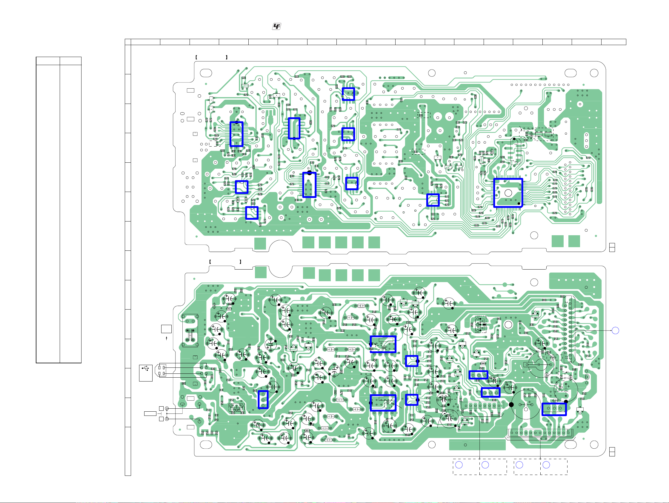
5-3. PRINTED WIRING BOARD – MAIN Board – :Uses unleaded solder.
• Semiconductor
Location
Ref. No. Location
D391 M-15
D393 D-15
D394 L-15
D397 D-14
D506 F-4
D507 F-4
D508 I-4
D509 I-3
D802 D-13
D803 K-12
D804 D-14
D805 K-15
D806 L-15
DZ502 N-6
IC301 C-6
IC302 E-7
IC303 E-8
IC304 D-8
IC305 B-8
IC306 K-9
IC307 M-9
IC308 K-10
IC309 M-10
IC310 F-11
IC391 L-13
IC392 M-15
IC501 D-4
IC502 M-5
IC505 F-5
IC506 E-4
IC801 F-13
IC802 L-12
Q301 J-14
Q302 I-10
Q303 I-10
Q304 K-6
Q305 E-12
Q306 E-11
Q307 K-11
Q308 L-12
Q309 L-12
Q310 M-12
Q312 D-11
Q313 K-12
Q391 L-16
Q392 M-16
Q501 B-3
Q502 C-3
Q506 B-5
Q507 B-4
Q508 K-7
Q801 D-12
Q802 K-12
1 2 3 4 5 6 7 8 9 10 11 12 13 14 15 16 17
A
B
C
D
E
MAIN BOARD
Q501
Q502
R506
R502
C506
(EXCEPT US)
F
G
H
I
D509
C523
J301
S801
AUTO
POWER
OFF
ON
124
3
L
R
S801
C532
R304
C533
C520
FB504
FB503
FB502
R301
R302
R305
-1 -2
FB303
J
K
J501
USB
ONLY 2ch
SOURCE
L
M
AUDIO IN
N
(COMPONENT SIDE)
E
E
IC501
R507
1
R537
R503
14
C511
R529
C513
R519
R528
R510
R513
IC506
1
R512
C515
4
C528
R525
R523
MAIN BOARD
C522
R527
D508
R511
R538
FB501
R509
C512
R504
R505
C303
C505
R303
C304
R306
R535
Q507
E
R534
28
C510
15
R518
C514
C531
R515
R514
R516
8
5
D506
D507
1
C526
4
(CONDUCTOR SIDE)
R531
R530
R539
FB507
C519
C509
FB505
X501
C507
C525
R524
C527
FB506
R522
R508
R517
C517
R526
8
IC505
5
C518
3
1
C524
R536
R521
C516
C501
C503
IC502
C521
C316
C315
Q506
R334
E
FB302
C529
R307
R350
8
14
R367
R370
C308
R308
R365
C307
C306
7
1
IC301
1
C312
R311
12
IC302
C324
C397
R310
E
Q304
C300
R366
R368
R533
C317
C305
DZ502
C395
Q508
R369
FB301
C311
C327
24
13
C396
E
C313
C314
C318
R313
R312
C336
C321
R329
R324
C323
C332
R330
14
R328
IC305
R327
85
C350
14
R325
IC304
85
R321
R319
R316
R335
R336
R333
C329
R317
C322
R315
R314
R320
R322
C333
14
IC303
85
C328
R318
(EXCEPT US)
C326
R345
C331
C343
C346
R323
IC307
C334
C342
C348
C351
R342
Q302
C302
R309
R344
C344
R339
IC306
14
C337
85
R338
R340
14
85
R341
FB304
C335
R346
C352
C345
C349
IC309
(EXCEPT US)
C392
C366
C355
C367
E
R348
C301
R352
C354
IC308
4
C358
R361
R343
(EXCEPT US)
IC310
Q303
R347
1
85
R349
R355
C359
14
85
C347
C369
(EXCEPT US)
C370
R385
C383
E
C381
C353
R351
R353
R356
R354
R358
R357
R359
R362
R360
C360
Q312
C382
C384
R388
C356
C357
R363
(EXCEPT US)
FB305
31
CN801
FB807
FB808
(EXCEPT US)
D394
C394
Q392
E
R882
R827
R826
1-860-898-12(12)
R814
R816
E
Q391
R396
R395
1-860-898-
(Page 16)
(12)
C
DISPLAY
BOARD
CN701
12
FB311
R849
C805
Q801
R836
R846
R848
X801
CN301
R875
R874
C804
E
R850
R851
R871
D803
13
C378
C376
A2
(Page 20)
D802
C803
R834
33
48
R844
R872
C806
FB313
AMP BOARD
CNP401
R853
FB802
13
FB308
R878
R877
R839
8
C375
IC801
R856
R854
R855
R876
C391
(EXCEPT US)
CN802
R858
R857
AAKAA
D804
D397
R391
C310
(US)
E
Q301
R390
(EXCEPT US)
FB307
C802
C809
+
C808
D806
C393
D393
D391
K
R397
FB804
(FOR CHECK)
1732
16
1
6449
C807
FB801
(EXCEPT US)
R392
C330
IC392
CN302
AMP BOARD
B1
(Page 18)
(US) (EXCEPT US)
CNP423
B2
(Page 20)
R815
R813
R811
R807
R805
R803
R801
R802
R804
R806
R808
R812
R810
D805
FB806
R398
(US)
AMP BOARD
CNP423
FB306
R399
C374
C373
C371
E
Q306
R383
14
85
C386
C385
R371
E
Q307
R372
R375
R376
R379
R378
R377
C362
C361
R364
C365
C363
R382
R380
C372
R374
R373
R843
EE
Q305
R384
R386
R387
R847
R852
R840
R833
Q313
E
E
Q802
E
Q309
C368
R873
E
Q308
IC802
FB309
(EXCEPT US)
IC391
FB310
1
FB312
C377
E
Q310
R381
AMP BOARD
A1
CNP401
(Page 18)
(US) (EXCEPT US)
R326
C319
C320
R332
R331
C325
R337
C338
C340
1212
Page 13

5-4. SCHEMATIC DIAGRAM – MAIN Board (1/3) – • See page 11 for IC Block Diagrams.
SS-US301/SW-US301/UZ-US301
ONLY 2ch SOURCE
AUDIO IN
(1/3)
C507
22p
R504
1M
R509 C505
1M 22p
J501
USB
J301
2P
R
L
GND
1
D+
D-
VBUS
4
FB303
R508
100
FB504
FB504
(EXCEPT US)
S)
0
(U
R305
R301 R303 C303
10k 47k 220p
R302
10k
FB506
FB501
FB502
FB503
0
FB303
0
0
(US)
R507
100k
Q502 Q501
2SC2712 DTA124EKA
USB CONTROL
SWITCH
+3.3V REGULATOR
IC502
S)
S-81233SGY
T U
EP
C
X
(E
C305
1
FB301
50V10k
C304R306R304
FB507
220p47k10k
FB302
C306
1
50V
R350
100k
R370
R367
R369
R368
R505
1k
100k
100k
100k
100k
R365
3.3k
X501
12MHz
D/A CONVERTER
IC501
PMC2704
R503
R502
R506
1.5k
USB CONTROL
SWITCH
C307
100
10V
USB
R366
100k
R537
1.5k
22
22
(US)
FB505
0
FB505
C503
47
25V
(EXCEPT US)
C506
220p
C509
0.1
R307
4.7k
)
S
T U
CEP
(EX
INPUT SELECTOR
C512
0.1
C533
1
50V
R513
10k
R514
1k
C516
1
50V
IC301
BU4066BCF
R511
R512
4.7k
C515
100p
A1
(Page 14)
A2
A3
A4
A5
A6
A7
C395
C521
10
50V
R334
1k
100
16V
C501
47
16V
R538
100
10k
C510
0.22
C520
100
10V
D
N
G
R529
3.3k
R519
C531
0.22
R523C526
470k470p
R528
3.3k
C511
0.22
R518C514
220.022
C519
C517
100p
R517
C518
C397
100
10V
R510
10k
C532
1
50V
R515
4.7k
R516
10k
1k
1
50V
R308
10k
0.1
C513
22
0.022
USB AMP
IC506
µPC457062
GND
VDD
D
D
V
C300
R539
100
0.1
C524
4.7
50V
R525
100
C528
0.22
R534
R533
1k
C525
4.7
50V
C313
1
50V
C314
1
50V
C315 C316
10
50V
C324
0.001
D506
1SS355
C523
D508
1
1SS355
50V
C317
4.7
50V
C311
0.0033
C312
0.0033
R311
4.7k
10
50V
R331
47k
R522
10k
R312
4.7k
C522
10
50V
BUFFER
IC505
µPC457DG2
GND
R527
220k
R531
100k1k
Q507
2SC2712
LINE AMP
QS7779CM-G-E2
3D SOUND PROCESSOR
VDD
IC302
R521
10k
C527R524
470p470k
R526
D507
1SS355
100
D509
1SS355
R530
∗
(US)
100k
(EXCEPT US)
68k
R535
470k
R530
C529
∗
0.22
C318
4.7
50V
R313 R536
4.7k 470k
C319
0.01
C320
0.01
R333
47k
R332
47k
C323
0.001
C321
C322
100
0.001
10V
Q506
2SC2712
LINE AMP
DZ502C327
UDZSTE-1780.001
B6
B4
B2
B1
B3
B5
B7
B8
(Page 15)
1313
Page 14
SS-US301/SW-US301/UZ-US301
5-5. SCHEMATIC DIAGRAM – MAIN Board (2/3) – • See page 11 for IC Block Diagrams.
(Page 13)
C301C325R314 R345
(2/3)
1k1 50V
1SS355
R397
R338C343
ELECTRICAL
VOLUME
IC306
M62429P
S)
T U
EP
C337
0.001
(EXC
R344
1k
R339
C344
1k
1
50V
C346
1
50V
R340
1k
(EXCEPT US)
R341
1k
C335
C348
1
50V
D806
(US)
(US)(EXCEPT US)
D804
0
1SS355
FB804
0.001
)
S
U
)
S
0
EPT
FB304
FB304
R398
0
(U
XC
(E
Q391
KTA1273Y-AT
B+ SWITCH
C352
ELECTRICAL
R342
1k
C350
0.001
C351
0.001
C366 C367
0.001 0.001
1 50V
R343
1k
VOLUME
IC307
M62429P
0
R317 R318
2.2k 0
C329
0.15
47 16V
10k
22 25V
FILTER
IC305
018k0.15
0.001
C808
0.22F
5.5V
C342
0.018
C326
0.15
GND
GND
C338R327C336
0.221k0.47
GND
(EXCEPT US)
VDD
R319C328
33k0.022
R321
10k
VDD
100k
R325
100k
R326
VDD
D805
R810C809
R810
0
(US)
(EXCEPT US)
∗
1DD355
∗
100
R315
A1
HIGH-PASS
FILTER
IC303
µPC4570G2
C331
R320
C332
HIGH-PASS
FILTER
IC304
µPC4570G2
A2
A3
1k
1k
R336
R335
R328
A4
A5
A6
A7
18k
R322 R323 R324C333R337
C334
2.2k 0 33k0.0220
0.15
LOW-PASS
µPC4570G2
R330R329C340
33k
R316
R396
10k
R395
1k
B+ SWITCH
829
830
828
827
Q392
DTC114EKA
)
S
U
EPT
C
X
(E
RB411D
(EXCEPT US)
1 50V0.0222.2k 1k
C302
1
50V
R353
47k
R356
47k
C345
1
50V
R354
3.3k
C349
1
50V
R364
4.7k
C361
R362
47k
0.1
C362
220
16V
C347
1
50V
C308
0.001
R363
4.7k
C369
0.001
C365
100p
C363
220
25V
D397
RB411D
R399
0
R347
1k
R348
100k
DTC343TK
MUTING
R309
100k
R346
1k
R351
3.3k
GND
VDD
C355
100p
R355
22k
R359 R357 R349 R358
47k 3.3k 10k 10k
GND
VDD
C358
100p
R360 R361
3.3k 10k
D393
+5.6V REGULATOR
D394
1SS355
C394
470
16V
R352
C354
100p
C359
KIA7805API
IC392
22k
100p
G
DTC343TK
MUTING
C370
0.001
(EXCEPT US)
PRE AMP
IC308
µPC4570G2
PRE AMP
IC309
µPC4570G2
IO
Q303
Q302
DTC124EKA
C381
50V
Q312,313
MUTING CONTROL
SWITCH
Q312
DTA124EKA
Q313
C393D391
0.11SS355
1
C353
1
50V
R385
R384
47k
1k
R386
47k
C383
1
50V
0
FB307
(US)
FB307
(EXCEPT US)
R371
R373
2.2k
10k
C371
0.001
C372
0.001
R374
10k
C356
1
50V 2.2k
C357
1
50V 2.2k
R379
10k
C373
0.001
C374
0.001
R380
10k
C360
1
50V 2.2k
DTA124EKA
KIA78L05BP
C392
100
10V
IC391
R388
Q305
G
C382
GND
C384R387
47p1k
2SD1938
MUTING
2SD1938
MUTING
2SD1938
MUTING
2SD1938
MUTING
IO
10k
Q307
Q308
Q309
Q310
DTC124EKA
REGULATOR
R383
10k
47p
VDD
R375
R377
R382
Q305,306
MUTING CONTROL
SWITCH
Q306
+5V
C385
100
10V
C386
100
10V
R372
100k
R376
100k
(US)
FB305
FB305
(EXCEPT US)
HEADPHONE AMP
µPC4570G2
(US)
FB306
FB306
(EXCEPT US)
(EXCEPT US)
(EXCEPT US)
(EXCEPT US)
R378
100k
R381
100k
(EXCEPT US)
R390
470
R391
R392
47
25V
HP.L
0
IC310
0
HP.R
GND
(US)
FB308
0
FB308
C375
0.001
C376
0.001
(US)
FB309
0
FB309
(US)
FB310
0
FB310
C377
0.001
C378
0.0022
(US)
FB311
0
FB311
470
470
C330C391
2200
16V
(EXCEPT US)
(EXCEPT US)
(US)
FB313
FB313
(US)
FB312
FB312
READY-H
SUB UNSW 5.6V
READY 10V
AMP-MUTE
A-GND
WOFER
A-GND
D-GND
P.CONT
DIG 10V
DIG 10V
A-GND
A-GND
CN301
CN302
0
0
(US)
8P
FR
(Page 19)
FL
C
(Page 21)
(EXCEPT US)
13P
(US)
(Page 19)
NC
NC
NC
(Page 21)
(EXCEPT US)
6
C5
C4
C3
C2
C1
C
7
C
C8
9
C
C12
C11
C10
(Page 15)
1414
Page 15

5-6. SCHEMATIC DIAGRAM – MAIN Board (3/3) – • See page 10 for Waveform. • See page 23 for IC Pin Function Description.
(Page 13)
SS-US301/SW-US301/UZ-US301
(Page 17)
CN801
23P
GND
HP.R
GND
HP.L
H/P-SW
H/P-MUTE
KEY1
KEY2
S-HIGH
S-LOW
GRN-LED
V-7
V-6
V-5
V-4
V-3
V-2
V-1
USB
RED-LED
EVER 5.0V
GND
READY 5.6V
-1
-2
S801
AUTO
POWER
OFF
6
1
B
B2
3
B
B4
5
B
7
B
B
8
B
(3/3)
C396
0.1
Q508
Q304,508
INPUT SELECTOR
CONTROL SWITCH
803
804
805
806
807
808
811
812
813
814
815
816
DTA124EK
Q304
DTC124EKA
100
R802
100
R803
100
R804
100
R805
100
R806
100
R807
100
R808
100
R811
100
R812
100
R813
100
R814
100
R815
100
R816
C308
0.001
C1
C2
FB801
R854
100
R853
R858
100
100
100
57
56
8
R8
R
SYSTEM CONTROLLER
IC801
µP0780022AGK
-C02-9ET
100
55
8
R
100
R852
100
R851
100
R850
100
R849
100
830
829
828
827
C802
220
10V
R848
100
R847
100
R846
100
R871
R844
100
R843
47k
FB802
R840
X801
1M
8.38MHz
100
C803
0.001
R839
0
R834R836
22k
R833
100
Q801
2SC2712
RESET
SWITCH
D802 R875
1SS355 47k
R874 C804
10k 0.22
5
3
C805
35
80
S
0.1
D
1S
47k
Q802
DTC124EKA
KEY ACTIVE
SWITCH
R873
10k
GVRST
RESET SIGNAL
GENERATOR
IC802
PST592C
C806
1
50V
R872
100
C5
C3
C4
C12
C8
C11
C6
(Page 14)
R310
10k
ON
Q301
DTA124EKA
MUTING
CONTROL
SWITCH
C807C310R801
0.0010.1100
FB808
HP.R
HP.L
R826
100
R827
100
803
804
805
806
807
808
811
812
813
814
815
816
R882
GND
100k
100k
10k
877
878
R
R
806
FB
(FOR CHECK)
CN802
R876
100k
8P
IN
OUT
2PIN
VPP
CLK
RESET
GND
VDD
FB807
C10
C9
C7
1515
Page 16

SS-US301/SW-US301/UZ-US301
5-7. PRINTED WIRING BOARD – DISPLAY Board – :Uses unleaded solder.
• Semiconductor
Location
Ref. No. Location
D701 C-11
D702 F-11
D703 G-9
D704 G-8
D705 G-7
D706 G-7
D707 G-6
D708 G-6
D709 G-5
D711 F-7
D712 F-6
Q701 G-11
Q702 G-10
Q707 G-6
Q708 G-6
Q709 G-5
Q710 G-10
Q711 F-5
Q712 F-6
Q751 C-11
Q752 F-11
1 2 3 4 5 6 7 8 9 10 11 12 13
A
B
DISPLAY BOARD
C
D
(COMPONENT SIDE)
R703
R707
R711
R701
R705
R709
D701
R715
FB751
R751
C752
R716
FB754
C751
FB734
Q751
E
C753
R752
L731
D701
K
A
K
A
1-860-899-
(POWER ON (GRN))
(STANDBY (RED))
12
(12)
MAIN BOARD
C
CN801
R725
CN701
D712
R724
D707
+4dB
D708
6
Q707
E
(Page 12)
R723
D706
WOOFER LEVEL
+2dB
D707
5
VOLUME
D711
0
D706
4
–2dB
D705
3
R722
D705
–4dB
D704
FB752
SURROUND MODE 12
R720R721
D704
–6dB
D703
1
2
D711D712
D703
FB753
R753
C754
FB736
R754
Q702
E
R731
S702
USB/AUDIO IN
R719
R755
E
Q710
R718
FB735
D702
USB
R717
R730
E
Q752
C756
Q701
E
1-860-899-
L732
S701
C755
12
(12)
J701
PHONES
E
DISPLAY BOARD
FB702
F
S705
S705
+
G
VOLUME
–
S706
FB701
FB703
S706
H
I
(CONDUCTOR SIDE)
S703
WOOFER
R702
R734
R735
R733
R732
S704
S-MODE
R704
R706
R710
R708
R712
R714
R713
Q711
E
Q709
D709
R726
D708
Q712
E
Q708
EE
+6dB
D709
7
R729
R728
1616
Page 17

5-8. SCHEMATIC DIAGRAM – DISPLAY Board –
SS-US301/SW-US301/UZ-US301
J701
PHONES
(CHASSIS)
FB736
CLP301
L731
33µH
C756 C753
0.1 0.01
C755
0.01
S-HIGH
Q712 Q711 Q709 Q708 Q707
DTC124EKA DTC124EKA DTC124EKA DTC124EKA DTC124EKA
LED
DRIVE
SURROUND MODE
Q751
DTC343TK
MUTING
Q752
DTC343TK
MUTING
V-4
R728R729
470470
LED
DRIVE
D711D712 D702
SLR-342MGT32SLR-342DUT32 SLR-342VRT32
V-3
S-LOW
R722R723
330330
DRIVE
7 6 5 4 3 2 1
FB734
FB735
V-7
V-2
LED
WOOFER LEVEL
0
D706D709 D708 D707 D705 D704 D703
VOLUME
R752
4.7k
R754
4.7k 0.1
L732
33µH
V-6
V-1
SLR-342MGT32SLR-342MGT32SLR-342MGT32SLR-342MGT32
R721 R720
330 330
R724R725R726
470470470
LED
DRIVE
D708D709 D707
SLR-342MGT32SLR-342MGT32 SLR-342MGT32
-6dB-4dB-2dB+2dB+4dB+6dB
DRIVE
USB/AUDIO IN
D703D704D705D706
LED
C751
S702
C752
0.0047
R751
33
R753
33
C754
0.0047
V-5
DTC124EKA DTC124EKA
DRIVE
R731 R730
USB
R718R719
470470
Q702 Q710
LED
USB2 1
(POWER ON(GRN))
10k 1k
S701
DRIVE
LED
GRN-LED
D701
SML-020MLTT86
(STANDBY(RED))
RED-LED
Q701
DTC124EKA
LED
DRIVE
R755
47k
R717
1k
S-HIGH
S-LOW
GRN-LED
V-7
V-6
V-5
V-4
V-3
V-2
V-1
USB
RED-LED
FB754
FB753
FB751
FB752
R716
R715
R714
R713
R712
R711
R710
R709
R708
R707
R706
R705
R704
R703
R702
R701
FB703
FB702
FB701
CN701
GND
HP.R
GND
100
100
100
100
100
100
100
100
100
100
0
0
0
0
100
100
HP.L
H/P-SW
H/P-MUTE
KEY1
KEY2
S-HIGH
S-LOW
GRN-LED
V-7
V-6
V-5
V-4
V-3
V-2
V-1
USB
RED-LED
EVER 5.0V
GND
READY 5.6V
23P
(Page 15)
VOLUME
R733R734R735 R732
22k47k100k 1k
S703S704S705S706
WOOFERS-MODE+-
1717
Page 18
SS-US301/SW-US301/UZ-US301
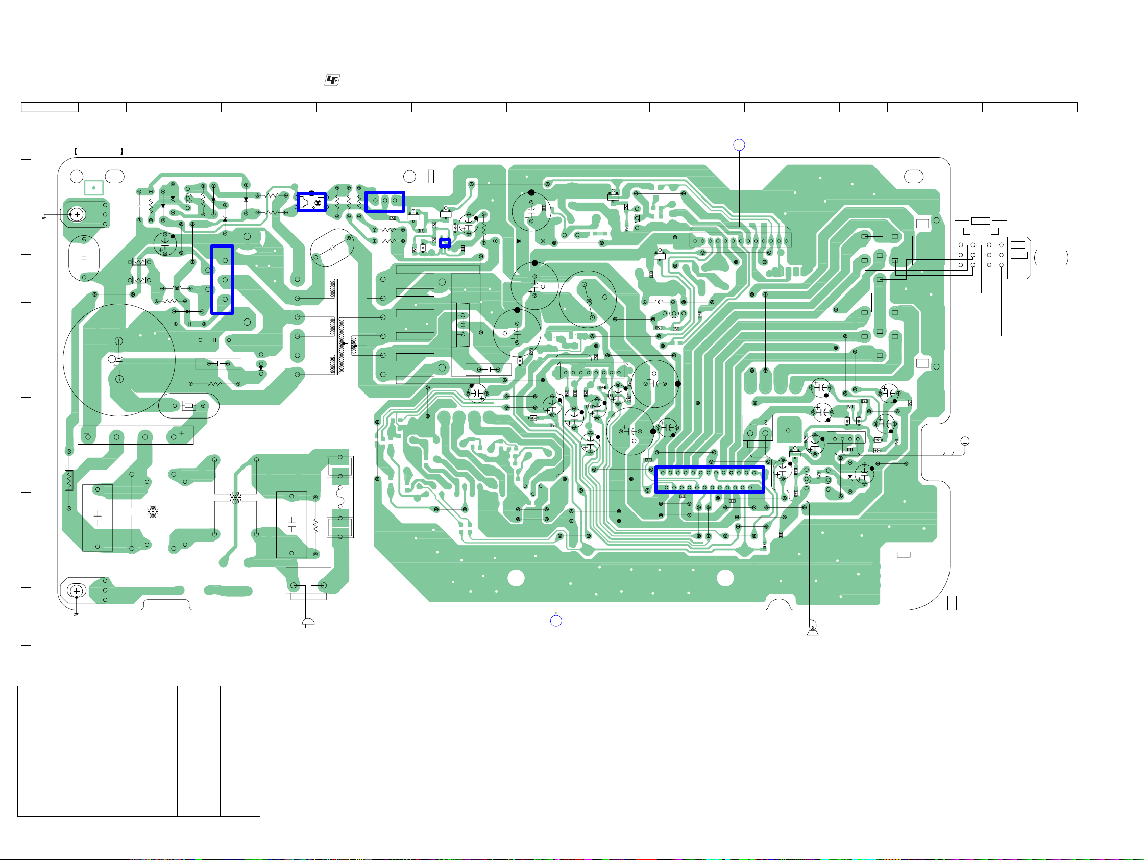
5-9. PRINTED WIRING BOARD – AMP Board (US model) – :Uses unleaded solder.
1 2 3 4 5 6 7 8 9 10 11 12 13 14 15 16 17 18 19 20 21 22
A
AMP BOARD
R911
D907
D904
C914
R901
EB901
C915
B
(CHASSIS)
C
C901
D
R903
R900
JW401
FB901
Q901
D901
JW402
C903
R907
D906
E
JW403
4
2
E
C912
F
TH901
IC901
C916
C913
R909
D903
D905
R913
R912
PC901
5
1
D908
R914
C911
T901
MAIN POWER
TRANSFORMER
R917
R920
IC902
13
R915
R919
R918
R922
E
Q902
C924
D910
E
Q906
R916
5
4
D914
R921
13
C919
IC903
D911
JW417
G
D902
H
R908
C904
I
LF902
14
JW452
FH901
R930
F901
JW420 JW422
FH902
LF901
C902
C929
JW405
C917
C931
R923
D909
JW406
C922
JW404
A
K
A
C920
C402
D402
JW418
JW419
C921
R404
JW416
D401
JW421
L901
18
R407
C472
C473
C401
R401
C405
JW423
R408
CNP401
C403
JW425
JW424
R425
C406
Q910
C470
R405
JW431
JW426
E
R931
R929
JW413
C404
JW427
JW412
JW414
JW415
C471
C923
R406
Q909
JW407
E
E
Q905
C932
L903
E
R932
C981
C424
1
113
JW410
JW411
Q904
R933
C409
2
JW433
JW432
C408
JW434
R423
IC401
JW448
JW447
JW435
B1
CNP423
JW449
JW444
JW446
C407
MAIN BOARD
CN302
JW408
JW409
CN401
1
24
JW443
JW445
JW455
JW436
2
25
C421
(Page 12)
JW437
E
Q452
R452
C410
R451
JW442
C422
R453
Q451
J404
SPEAKER
–
–
–
43 1
R L
+
+
+
FAN902
M
(FAN)
+
–
FRONT
CENTER
TO SATELLITE
SPEAKER (L)/ (R)
(SS-US301)
+
–
+
–
15
3
6
JW438
12
JW439
C455
C458
C451
R458
E
Q453
JW440
R455
R454
D451
D454
CN421
14
C454
4
13
JW450
C453
E
D947
4
9
10
JW441
D453
D452
2
711
8
C457
R456
C456
R457
JW453
J
CN902
(AC IN)
1
11
(11)
MAIN BOARD
A1
(Page 12)
CN301
12
SP101
(SUB WOOFER)
1-860-900-
2
EB902
K
(CHASSIS)
• Semiconductor Location
Ref. No. LocationRef. No. Location
D401 G-11
D402 F-11
D451 G-18
D452 H-18
D453 G-18
D454 G-18
D901 E-4
D902 G-3
D903 C-5
D904 B-3
D905 B-5
D906 B-4
D907 B-3
D908 F-5
D909 C-11
D910 C-9
D911 E-10
D914 C-9
D947 H-18
IC401 H-15
IC901 D-5
IC902 B-8
IC903 C-9
Ref. No. Location
PC901 B-6
Q451 H-17
Q452 H-17
Q453 H-17
Q901 B-4
Q902 C-9
Q904 E-14
Q905 D-14
Q906 C-9
Q909 C-13
Q910 B-13
1818
Page 19

5-10. SCHEMATIC DIAGRAM – AMP Board (US model) – • See page 11 for IC Block Diagram.
C920
3300p
L901
FMB-26L
630V
Q904
KTA1271Y-AT
B+ SWITCH
R933
R932
10k
D911
V
V
5
25
2
0
00
0
2
2
2
2
1
22
92
9
C
C
1k
Q905
DTC114EKA
B+ SWITCH
C981C923
2200
2200
25V
25V
(AC IN)
(CHASSIS)
F901
CN902
5A
2P
125V
R930
3.3M
1/2W
IC901
STR-F6424
POWER CONTROL
0.0022
EB901
LF901
C902
0.1
250V
C901
250V
LF902
R908
68k
2W
C914
47
50V
W
2
0
V
2
4
0
.2
0
K
A
3
0
9
901
R
D
R912
5.6k
11EQS10
AG01Z
FB901
W
2
2
0.2
00
9
R
C903
220p
D907
C904
0.1
250V
R901
680
p
00
1
15
9
C
D905
11EQS10
AG01Z
D902
RBV-406
2
41
3
D904
MTZJ20B
REGULATOR
R911
2.7k
PC901
TLP421
ISOLATOR
Q901
2SD1616
+20V
TH901
C912
330
200V
11EQS10AG01Z
R907
4.7k
MTZJ20B
R909
C913
82k
3300p
1/2W
630V
D908
SARS03
R913
D906
22
C916
1500p
2kV
T901
MAIN POWER
TRANSFORMER
D903
C911
0.0022
250V
R917 R918
470 220
R919
R914
10k
2.7k
R920
4.7k
SS-US301/SW-US301/UZ-US301
CN401
C409 C410
47
C421
0.1
WOFER
POWER AMP
C402
0.1
50V
C
FR
FL
IC401
TDA7386
C403
0.1
50V
R405
C470
1k
0.001
C404
0.1
50V
R406
C471
1k
0.001
C405
0.1
50V
R407
C472
1k
0.001
C406
0.1
50V
R408
C473
1k
0.001
C401
C424
2.2
0.1
50V
R451
C422C408C407
100000p100000p100000p
L903
4.7µH10µH
C932
100000p
0.47
25V
50V
0V
0V
0V
5
5
5
0
10
10
1
56
57
55
4
4
C
C4
C
R454
470
R455
Q451
KTA1271Y
-AT
B+ SWITCH
R452
2SC2712
1k
Q452
10k
B+ SWITCH
470
R456
470
R457
470
R453
47
C451
10
50V
5
5
35
355
S
S35
S
S
1S
1
1S
3
52
51
4
45
4
D
D
D
R458
220
C453 D947
10
MTZJ-T-77
50V
2P
5
6
11
12
3
4
9
10
2
1
KTC3205-Y
+10V
REGULATOR
8
7
Q453
C454
0.1
V
0
5
10
58
C4
355
S
1S
4
45
D
-10B
SP101
(WOOFER)
J404
SPEAKER
R L
FRONT
TO SATELLITE
CENTER
SPEAKER(L)/(R)
(SS-US301)
CN421
4P
FAN902
(FAN)
(Page 14)
REF
C
IC902
GND
SE-B2
SWITCHING
R921 D910R916C924R915
33k 1SS3554.7k470p2.2k
R923
R922
IC903
220k
TC4S584F
5
3
2
4
Q902,906
POWER ON/OFF
CONTROL SWITCH
Q902
DTC124EKA
CNP423 Q906
13P DTC124EKA
D-GND
READY-H
P.CONT
DIG 10V
SUB UNSW 5.6V WOFER
READY 10V
NC
NC
DIG 10V
NC
AMP-MUTE
A-GND
A-GND
1
INVERTER
6.8
D914
1SS355
C929
C919
22
0.022
25V
D909
RK16
C917
C931
1000
0.1
16V
KTA1273Y-AT
B+ SWITCH
R931R929
1k10k
DTC114EKA
B+ SWITCH
Q909
R425
100K
R401
22k
D401
Q910
1SS355
R423
0
D402
R404
47k
1SS355
C
WOFER
FL
FR
A-GND
A-GND
CNP401
8P
FL
SR
SL
FR
C
(Page 14)
The components identified by mark 0 or dotted
line with mark 0 are critical for safety.
Replace only with part number specified.
1919
Page 20

SS-US301/SW-US301/UZ-US301
5-11. PRINTED WIRING BOARD – AMP Board (Except US model) – :Uses unleaded solder.
1 2 3 4 5 6 7 8 9 10 11 12 13 14 15 16 17 18 19 20 21 22
C410
C422
131
CN451
E
E
FB404
R452
R451
(SUB WOOFER)
SUB BOARD
CNP922
(Page 22)
14
FB406
C455
C458
C451
R453
Q452
R458
Q451
E
12
SP101
Q453
JW438
4 13
E
FB403
JW450
FB401
FB402
FB405
R454
CN421
C454
D947
JW439
D454
6
12
JW440
R455
14
C453
D451
JW441
J404
SPEAKER
–
–
–
43 1
21
(21)
R L
+
+
+
FAN902
M
(FAN)
+
–
FRONT
CENTER
TO SATELLITE
SPEAKER (L)/ (R)
(SS-US301)
+
–
+
–
15
3
2
4
711
9
8
10
C457
R456
C456
D453
R457
D452
JW453
1-860-900-
JW435
C403
D401
C470
JW427
CNP423
JW408
JW449
C404
C471
B2
JW409
1
C407
JW444
R406
MAIN BOARD
CN302
(Page 12)
JW436
CN401
2
24
JW445
JW416
JW437
C421
JW442
A
AMP BOARD
R911
D907
D904
Q901
R907
D906
E
EB901
C915
B
(CHASSIS)
C
JW402
JW403
C901
D
R903
R900
JW401
E
C912
F
G
H
I
R908
C904
D902
C914
4
FB901
R901
LF902
D901
C903
TH901
2
IC901
C916
C913
R909
14
D905
R913
D903
5
1
LF901
R912
D908
PC901
C902
C911
T901
MAIN POWER
TRANSFORMER
FH901
FH902
R930
R914
R917
R920
IC902
3
1
R919
R918
A
K
D911
A
JW417
JW452
F901
JW420 JW422
J
EB902
K
(CHASSIS)
CN902
D
12
SUB BOARD
CN991
(Page 22)
C920
JW404
JW405
A2
C917
D909
C922
C921
D402
JW421
MAIN BOARD
CN301
(Page 12)
C931
18
C402
R404
L901
CNP401
E
Q910
JW406
JW413
JW412
JW415
R931
Q909
E
R929
E
JW407
C932
E
JW433
JW432
R425
L903
R401
C401
JW434
IC401
C408
C406
C405
JW426
JW448
JW447
R408
R407
R405
C473
C472
Q905
R933
R932
Q904
C981
C923
C409
C424
125
2
JW446
• Semiconductor Location
Ref. No. LocationRef. No. Location
D401 D-15
D402 G-11
D451 G-18
D452 H-18
D453 G-18
D454 G-18
D901 E-4
D902 G-3
D903 C-5
D904 B-4
D905 B-5
D906 B-4
D907 B-3
D908 F-5
D909 C-11
D911 E-10
D947 H-18
IC401 H-15
IC901 D-5
IC902 B-8
PC901 B-6
Ref. No. Location
Q451 H-17
Q452 H-17
Q453 H-17
Q901 B-4
Q904 D-14
Q905 D-14
Q909 C-13
Q910 B-13
2020
Page 21

5-12. SCHEMATIC DIAGRAM – AMP Board (Except US model) – • See page 11 for IC Block Diagram.
C920
3300p
(Page 22)
(CHASSIS)
CN902
EB901
CN451
RELAY ON
+5.6V
L901
FMB-26L
630V
R932
D911
10k
V
V
5
2
25
0
00
0
2
2
22
1
2
2
2
9
9
C
C
2200
25V
F901
T3.15AL
250V
2P
R930
3.3M
1/2W
IC901
STR-F6676
POWER CONTROL
4P
LF901
C902
0.1
250V
C901
0.001
250V
LF902
R908
68k
2W
C914
47
50V
W
2
0
7
4V
0
.4
0
K
A
3
0
1
9
90
R
D
R912
5.6k
11EQS10
AG01Z
FB901
W
2
3
0.3
00
9
R
C903
220p
D907
C904
0.1
250V
R901
680
R911
2.7k
p
00
1
15
9
C
D905
11EQS10
AG01Z
TLP421
ISOLATOR
D902
RBV-406
2
41
3
D904
MTZJ20B
Q901
2SD1616
+20V
REGULATOR
PC901
TH901
C912
220
400V
11EQS10AG01Z
R907
4.7k
MTZJ20B
D903
C913
3300p
630V
SARS03
D906
R909
82k
1/2W
D908
C916
1500p
2kV
R917 R918
470 220
R914
2.7k
R913
22
T901
MAIN POWER
TRANSFORMER
C911
0.001
250V
R919
10k
R920
4.7k
KTA1271Y-AT
B+ SWITCH
R933
1k
DTC114EKA
B+ SWITCH
L903
4.7µH10µH
Q904
Q905
C932
C981C923
2200
25V
100000p
SS-US301/SW-US301/UZ-US301
CN401
C409 C410
47
C421
0.1
POWER AMP
C402
0.1
50V
WOFER
C
R425
100k
R401
22k
D401
1SS355
FR
FL
IC401
TDA7386
C403
100000p
C470
R405
0.001
1k
C404
100000p
C471
R406
1k
0.001
C405
100000p
C472
R407
0.001
1k
C406
100000p
C473
R408
0.001
1k
C401
C424
2.2
0.1
50V
C422C408C407
100000p100000p100000p
0.47
25V
50V
FB405
FB406
FB401
FB402
FB403
FB404
R454
Q451
KTA1271Y
-AT
B+ SWITCH
2SC2712
R452
Q452
R451
10k
B+ SWITCH
R455
R456
R457
1k
R453
47
C451
10
50V
0V
50V
5
50V
0
10
1
10
7
55
456
45
4
C
C
C
470
470
470
470
5
55
35
3
355
S
S
S
1S
1SS
1
3
52
5
51
4
4
4
D
D
D
R458
220
MTZJ-T-77
C453
10
50V
2P
5
6
11
12
3
4
9
10
2
1
KTC3205-Y
+10V
REGULATOR
8
7
Q453
C454
0.1
0V
5
0
1
58
4
C
5
S35
S
1
54
4
D
D947
-10B
SP101
(WOOFER)
J404
SPEAKER
R L
FRONT
TO SATELLITE
CENTER
SPEAKER(L)/(R)
(SS-US301)
CN421
4P
FAN902
(FAN)
(Page 22)
(Page 14)
SUB.GND
SWITCHING
CNP423
13P
D-GND
READY-H
P.CONT
DIG 10V
SUB UNSW 5.6V WOFER
READY 10V
NC
NC
DIG 10V
NC
AMP-MUTE
A-GND
A-GND
REF
C
IC902
GND
SE-B2
D909
RK16
C917
C931
1000
0.1
16V
Q909
KTA1273Y-AT
B+ SWITCH
R931R929
1k10k
Q910
DTC114EKA
B+ SWITCH
1SS355
C
WOFER
FL
D402
R404
47k
FR
A-GND
A-GND
CNP401
8P
FL
SR
SL
FR
C
(Page 14)
The components identified by mark 0 or dotted
line with mark 0 are critical for safety.
Replace only with part number specified.
2121
Page 22

SS-US301/SW-US301/UZ-US301
5-13. PRINTED WIRING BOARD – SUB Board (Except US model) – :Uses unleaded solder.
1 2 3 4 5 6
AMP BOARD
E
CN451
A
B
SUB BOARD
R992
E
Q991
D991
R991
R995
RY991
D996
R994
R993
C994
Q992
E
JW903
R996
RY992
C991
(Page 20)
4
1
CNP992
JW901
JW902
C993
13
IC991
C
D992
5-14. SCHEMATIC DIAGRAM – SUB Board (Except US model) –
CN991
2P
(Page 21)
(AC IN)
LIVE
NEUTRAL
CN990
C992
0.01
250V
RY992
RY991
C991
0.01
250V
T902
SUB POWER
TRANSFORMER
D992
2P
LIVE
NEUTRAL
1SR154-400
D993
1SR154-400
1SS355
1SS355
D996
D991
D995
1SR154-400
D994
1SR154-400
R996
100
R995
100
+5.6V REGULATOR
IC991
S-81256PG-Z
IGO
C993
2200
16V
KTC3198GR
RELAY DRIVE
Q992
KTC3198GR
RELAY DRIVE
Q991
C994
100
10V
R993
10k
R991
10k
RELAY ON
SUB.GND
CNP992
4P
+5.6V
(Page 21)
R994
R992
100k
100k
D
CN990
1
CN991
2
D995
D993
D994
E
(AC IN)
2
1
T902
SUB POWER
TRANSFORMER
C992
F
AMP BOARD
D
CN902
1-860-897-
11
(11)
(Page 20)
• Semiconductor
Location
Ref. No. Location
D991 B-1
D992 D-6
D993 D-6
D994 E-6
D995 D-6
D996 B-3
IC991 B-5
Q991 B-2
Q992 B-2
The components identified by mark 0 or dotted
line with mark 0 are critical for safety.
Replace only with part number specified.
2222
Page 23

SS-US301/SW-US301/UZ-US301
• IC Pin Function Description
MAIN BOARD IC801 µPD780022AGK-C02-9ET (SYSTEM CONTROLLER)
Pin No. Pin Name I/O Description
1 H/P-S/W I
2H/P-MUTE O Headphone muting on/off control signal output terminal “H”: muting on
3 S-HIGH O
4 S-LOW O
5 GRN-LED O
6 V-7 O
7 V-6 O
8 V-5 O
9 VSS — Ground terminal
10 VDD — Power supply terminal (+5V)
11 V-4 O
12 V-3 O
13 V-2 O
14 V-1 O
15 USB-LED O
16 RED-LED O
17 to 23 — —
24 VDD — Power supply terminal (+5V)
25 AVSS —
26, 27 KEY1, KEY2 I
28 to 32 — —
33 AUDIO-DET I Audio level detection signal input terminal for auto power control
34 AVREF I
35 AVDD —
36 RESET I
37, 38 — —
39 IC (VPP) —
40 X2 O
41 X1 I
42 VSS1 — Ground terminal
43 STOP I
44 INT I Top key input detection signal input terminal with power save mode
45 — —
46 P-CON O Power on/off control signal output terminal “H”: power on
47 READY-H O Power on/off control signal output terminal with auto power control “H”: power on
48 AMP-MUTE O Muting on/off control signal output to the amplifier circuit “H”: muting on
49 VOL2-DATA O Serial data output to the electrical volume (for center and sub woofer)
50 VOL2-CLK O Serial data transfer clock signal output to the electrical volume (for center and sub woofer)
51 LINE-MUTE O
52 VOL1-DATA O Serial data output to the electrical volume (for front L-ch and R-ch)
53 VOL1-CLK O Serial data transfer clock signal output to the electrical volume (for front L-ch and R-ch)
54 S-TRB O Muting on/off control signal output to the 3D sound processor “H”: muting on
55 USB-H O Input selection signal output terminal “L”: AUDIO IN, “H”: USB
Headphone detection signal input terminal “H”: headphone in
LED drive signal output of sound mode high indicator “H”: LED on
LED drive signal output of sound mode low indicator “H”: LED on
LED drive signal output of power on indicator “H”: LED on
LED drive signal output of volume 7 indicator “H”: LED on
LED drive signal output of volume 6 indicator “H”: LED on
LED drive signal output of volume 5 indicator “H”: LED on
LED drive signal output of volume 4 indicator “H”: LED on
LED drive signal output of volume 3 indicator “H”: LED on
LED drive signal output of volume 2 indicator “H”: LED on
LED drive signal output of volume 1 indicator “H”: LED on
LED drive signal output of USB indicator “H”: LED on
LED drive signal output of standby indicator “H”: LED on
Not used
Ground terminal (for A/D converter)
Top panel key input terminal (A/D input)
Not used
Reference voltage (+5V) input terminal (for A/D converter)
Power supply terminal (+5V) (for A/D converter)
System reset signal input from the reset signal generator “L”: reset
For several hundreds msec. after the power supply rises, “L” is input, then it changes to “H”
Not used
Not used
System clock output terminal (8.38 MHz)
System clock input terminal (8.38 MHz)
AC cut detection signal input terminal
Not used
Line muting on/off control signal output terminal (for front L-ch and R-ch, sub woofer)
“H”: muting on
23
Page 24

SS-US301/SW-US301/UZ-US301
Pin No. Pin Name I/O Description
56 S-DATA O
57 S-CLK O
58
59
60 to 64 — —
APC-ON/OFF
C-MUTE
Bypass/Qsurround selection signal output to the 3D sound processor
“L”: Qsurround on, “H”: bypass on
Spread selection signal output to the 3D sound processor
“L”: spread minimum, “H”: spread maximum
I APC (auto power control) on/off switch input terminal “H”: APC on
O Line muting on/off control signal output terminal (for center) “H”: muting on
Not used
24
Page 25

SECTION 6
EXPLODED VIEWS
SS-US301/SW-US301/UZ-US301
NOTE:
• -XX and -X mean standardized parts, so they
may have some difference from the original
one.
• Color Indication of Appearance Parts
Example:
KNOB, BALANCE (WHITE) . . . (RED)
↑↑
Parts Color Cabinet's Color
6-1. OVERALL SECTION
2
1
• Items marked “*” are not stocked since they
are seldom required for routine service. Some
delay should be anticipated when ordering
these items.
• The mechanical parts with no reference number in the exploded views are not supplied.
• Accessories are given in the last of the electrical parts list.
#2
The components identified by
mark 0 or dotted line with mark
0 are critical for safety.
Replace only with part number
specified.
#2
#4
#2
#1
#1
1
3
#1
front cabinet section
#3
rear chassis
section
main section
Ref. No. Part No. Description Remark
1 4-221-580-01 SCREW, CASE
* 2 4-251-247-01 CHASSIS, TOP (EXCEPT US)
* 2 4-251-247-11 CHASSIS, TOP (US)
3 1-775-214-11 WIRE (FLAT TYPE) (23 CORE) (EXCEPT US)
3 WIRE (FLAT TYPE) (23 CORE) (US)
Ref. No. Part No. Description Remark
#1 7-685-646-79 SCREW +BVTP 3X8 TYPE2 IT-3
#2 7-685-647-79 SCREW +BVTP 3X10 TYPE2 IT-3
#3 7-685-872-09 SCREW +BVTT 3X8 (S)
#4 7-685-645-11 SCREW 3X6
25
Page 26

SS-US301/SW-US301/UZ-US301
6-2. FRONT CABINET SECTION
51
52
52
53
not supplied
Ref. No. Part No. Description Remark
* 51 A-4750-095-A DISPLAY BOARD, COMPLETE
52 4-951-620-11 SCREW (2.6X10), +BVTP
26
Ref. No. Part No. Description Remark
53 X-4956-253-1 CABINET SUB ASSY
Page 27

6-3. MAIN SECTION
102
F901
SS-US301/SW-US301/UZ-US301
#1
not supplied
#1
103
105
not supplied
101
#2
106
104
#1
Ref. No. Part No. Description Remark
101 X-4956-047-1 CABINET ASSY, SPEAKER (EXCEPT US)
101 X-4956-291-1 CABINET ASSY, SPEAKER (US)
* 102 A-4751-306-A AMP BOARD, COMPLETE (EXCEPT US)
* 102 A-4751-371-A AMP BOARD, COMPLETE (US)
* 103 A-4751-307-A MAIN BOARD, COMPLETE (EXCEPT US)
* 103 A-4751-373-A MAIN BOARD, COMPLETE (US)
104 4-238-407-11 SCREW (1) (4X20), +BV TAPPING
The components identified by mark 0 or dotted
line with mark 0 are critical for safety.
Replace only with part number specified.
Ref. No. Part No. Description Remark
105 3-252-835-01 CUSHION
106 3-846-312-01 SPACER
0 F901 1-532-465-31 FUSE (T3.15AL/250V) (EXCEPT US)
0 F901 1-533-453-12 FUSE, GLASS TUBE (DIA.5) (5A/125V) (US)
#1 7-685-646-79 SCREW +BVTP 3X8 TYPE2 IT-3
#2 7-685-647-79 SCREW +BVTP 3X10 TYPE2 IT-3
27
Page 28

SS-US301/SW-US301/UZ-US301
6-4. REAR CHASSIS SECTION
EXCEPT US
151
FAN902
154
152
#2
153
EXCEPT
US
#2
Ref. No. Part No. Description Remark
* 151 A-4751-309-A SUB BOARD, COMPLETE (EXCEPT US)
152 4-217-350-11 STOPPER, CORD
0153 1-696-169-51 CORD, POWER (EXCEPT US)
0153 1-783-531-81 CORD, POWER (US)
* 154 4-251-246-01 CHASSIS, REAR (US)
155
The components identified by mark 0 or dotted
line with mark 0 are critical for safety.
Replace only with part number specified.
Ref. No. Part No. Description Remark
154 4-251-246-11 CHASSIS, REAR (EXCEPT US)
155 4-251-699-01 SHEET, SPEAKER
FAN902 1-763-561-22 FAN, D.C.
#2 7-685-647-79 SCREW +BVTP 3X10 TYPE2 IT-3
28
Page 29

6-5. SS-US301 (L)/(R)
SS-US301/SW-US301/UZ-US301
201
202
203
Ref. No. Part No. Description Remark
201 A-4713-993-A SPEAKER ASSY (L), FRONT (EXCEPT US)
201 A-4714-059-A SPEAKER ASSY (L), FRONT (US)
202 A-4713-994-A SPEAKER ASSY (R), FRONT (EXCEPT US)
203
Ref. No. Part No. Description Remark
202 A-4714-060-A SPEAKER ASSY (R), FRONT (US)
203 4-239-498-01 FOOT
29
Page 30
SS-US301/SW-US301/UZ-US301
AMP
ELECTRICAL PARTS LIST
SECTION 7
NOTE:
•Due to standardization, replacements in the
parts list may be different from the parts specified in the diagrams or the components used
on the set.
• -XX and -X mean standardized parts, so they
may have some difference from the original
one.
• RESISTORS
All resistors are in ohms.
METAL: Metal-film resistor.
METAL OXIDE: Metal oxide-film resistor.
F: nonflammable
Ref. No. Part No. Description Remark Ref. No. Part No. Description Remark
* A-4751-306-A AMP BOARD, COMPLETE (EXCEPT US)
* A-4751-371-A AMP BOARD, COMPLETE (US)
*********************
1-533-313-11 FUSE HOLDER
< CAPACITOR >
C401 1-126-961-11 ELECT 2.2uF 20% 50V
C402 1-126-956-11 ELECT 0.1uF 20% 50V
C403 1-126-956-11 ELECT 0.1uF 20% 50V
C403 1-131-992-11 CERAMIC CHIP 100000PF 35V
C404 1-126-956-11 ELECT 0.1uF 20% 50V
C404 1-131-992-11 CERAMIC CHIP 100000PF 35V
C405 1-126-956-11 ELECT 0.1uF 20% 50V
C405 1-131-992-11 CERAMIC CHIP 100000PF 35V
C406 1-126-956-11 ELECT 0.1uF 20% 50V
C406 1-131-992-11 CERAMIC CHIP 100000PF 35V
C407 1-131-992-11 CERAMIC CHIP 100000PF 35V
C408 1-131-992-11 CERAMIC CHIP 100000PF 35V
C409 1-126-947-11 ELECT 47uF 20% 35V
C410 1-126-959-11 ELECT 0.47uF 20% 50V
C421 1-107-826-11 CERAMIC CHIP 0.1uF 10% 16V
• Items marked “*” are not stocked since they
are seldom required for routine service.
Some delay should be anticipated when ordering these items.
• SEMICONDUCTORS
In each case, u: µ, for example:
uA. . : µA. . uPA. . : µPA. .
uPB. . : µPB. . uPC. . : µPC. .
uPD. . : µPD. .
• CAPACITORS
uF: µF
• COILS
uH: µH
0 C901 1-113-907-51 CERAMIC 0.0022uF 20% 250V
0 C902 1-104-705-51 MYLAR 0.1uF 20% 250V
0 C903 1-162-282-31 CERAMIC 220PF 10% 50V
0 C904 1-104-705-51 MYLAR 0.1uF 20% 250V
0 C911 1-117-699-11 CERAMIC 0.001uF 99% 250V
0 C911 1-113-907-51 CERAMIC 0.0022uF 20% 250V
(US)
0 C912 1-115-586-11 ELECT (BLOCK) 220uF 20% 400V
(EXCEPT US)
(EXCEPT US)
(EXCEPT US)
(EXCEPT US)
0 C912 1-125-708-11 ELECT (BLOCK) 330uF 20% 200V
(US)
0 C913 1-117-452-11 FILM 3300PF 5% 630V
0 C914 1-126-967-11 ELECT 47uF 20% 50V
0 C915 1-162-282-31 CERAMIC 100PF 10% 50V
0 C916 1-125-772-51 CERAMIC 1500PF 10% 2KV
(US)
(US)
C917 1-126-767-11 ELECT 1000uF 20% 16V
C919 1-164-227-11 CERAMIC CHIP 0.022uF 10% 25V
C920 1-117-452-11 FILM 3300PF 5% 630V
C921 1-115-792-11 ELECT 0.0022F 20% 25V
C922 1-115-792-11 ELECT 0.0022F 20% 25V
C923 1-115-792-11 ELECT 0.0022F 20% 25V
C924 1-162-962-11 CERAMIC CHIP 470PF 10% 50V
C929 1-104-662-11 ELECT 22uF 20% 25V
C931 1-107-826-11 CERAMIC CHIP 0.1uF 10% 16V
The components identified by
mark 0 or dotted line with mark
0 are critical for safety.
Replace only with part number
specified.
When indicating parts by reference
number, please include the board.
(US)
(EXCEPT US)
(US)
(EXCEPT US)
(US)
(US)
(US)
(US)
C422 1-131-992-11 CERAMIC CHIP 100000PF 35V
C424 1-107-826-11 CERAMIC CHIP 0.1uF 10% 16V
C451 1-126-964-11 ELECT 10uF 20% 50V
C453 1-126-964-11 ELECT 10uF 20% 50V
C454 1-164-360-11 CERAMIC CHIP 0.1uF 16V
C455 1-126-964-11 ELECT 10uF 20% 50V
C456 1-126-964-11 ELECT 10uF 20% 50V
C457 1-126-964-11 ELECT 10uF 20% 50V
C458 1-126-964-11 ELECT 10uF 20% 50V
C470 1-162-964-11 CERAMIC CHIP 0.001uF 10% 50V
C471 1-162-964-11 CERAMIC CHIP 0.001uF 10% 50V
C472 1-162-964-11 CERAMIC CHIP 0.001uF 10% 50V
C473 1-162-964-11 CERAMIC CHIP 0.001uF 10% 50V
0C901 1-117-699-11 CERAMIC 0.001uF 99% 250V
(EXCEPT US)
30
C932 1-131-992-11 CERAMIC CHIP 100000PF 35V
C981 1-115-792-11 ELECT 0.0022F 20% 25V
< CONNECTOR >
CN401 1-564-320-00 PIN, CONNECTOR (3.96mm PITCH) 2P
* CN421 1-564-706-11 PIN, CONNECTOR (SMALL TYPE) 4P
CN451 1-784-921-11 PIN, CONNECTOR 4P (EXCEPT US)
CN902 1-564-321-00 PIN, CONNECTOR (3.96mm PITCH) 2P
< DIODE >
D401 8-719-988-61 DIODE 1SS355TE-17
D402 8-719-988-61 DIODE 1SS355TE-17
D451 8-719-988-61 DIODE 1SS355TE-17
D452 8-719-988-61 DIODE 1SS355TE-17
D453 8-719-988-61 DIODE 1SS355TE-17
Page 31
SS-US301/SW-US301/UZ-US301
AMP
Ref. No. Part No. Description Remark
D454 8-719-988-61 DIODE 1SS355TE-17
0 D901 8-719-043-76 DIODE AK04V0
0 D902 8-719-084-58 DIODE RBV-406
0 D903 8-719-110-53 DIODE RD20ESB2
0 D904 8-719-110-53 DIODE RD20ESB2
0 D905 8-719-200-91 DIODE 11EQS10
0 D906 8-719-200-91 DIODE 11EQS10
0 D907 8-719-200-91 DIODE 11EQS10
0 D908 6-500-241-01 DIODE SARS03
D909 6-500-258-01 DIODE RK16
D910 8-719-988-61 DIODE 1SS355TE-17 (US)
D911 8-719-080-05 DIODE FMB-26L
D914 8-719-988-61 DIODE 1SS355TE-17 (US)
D947 8-719-110-17 DIODE RD10ESB2
< GROUND TERMINAL >
EB901 1-537-770-21 TERMINAL BOARD, GROUND
EB902 1-537-770-21 TERMINAL BOARD, GROUND
< COIL >
FB401 1-400-160-51 INDUCTOR (SMALL TYPE) (EXCEPT US)
FB402 1-400-160-51 INDUCTOR (SMALL TYPE) (EXCEPT US)
FB403 1-400-160-51 INDUCTOR (SMALL TYPE) (EXCEPT US)
FB404 1-400-160-51 INDUCTOR (SMALL TYPE) (EXCEPT US)
FB405 1-400-160-51 INDUCTOR (SMALL TYPE) (EXCEPT US)
FB406 1-400-160-51 INDUCTOR (SMALL TYPE) (EXCEPT US)
0 FB901 1-412-473-21 INDUCTOR (SMALL TYPE)
< IC >
IC401 8-759-486-44 IC TDA7386
0 IC901 8-749-017-79 IC STR-F6676 (EXCEPT US)
0 IC901 8-749-018-45 IC STR-F6424 (US)
IC902 6-700-388-01 IC SE-B2
IC903 8-759-390-72 IC TC4S584F (TE85R) (US)
< TERMINAL BOARD >
Ref. No. Part No. Description Remark
Q904 8-729-037-13 TRANSISTOR KTA1271Y
Q905 8-729-027-43 TRANSISTOR DTC114EKA-T146
Q906 8-729-027-52 TRANSISTOR DTC124EKA-T146 (US)
Q909 8-729-040-76 TRANSISTOR KTA1273-Y-AT
Q910 8-729-027-43 TRANSISTOR DTC114EKA-T146
< RESISTOR >
R401 1-216-837-11 METAL CHIP 22K 5% 1/10W
R404 1-216-841-11 METAL CHIP 47K 5% 1/10W
R405 1-216-821-11 METAL CHIP 1K 5% 1/10W
R406 1-216-821-11 METAL CHIP 1K 5% 1/10W
R407 1-216-821-11 METAL CHIP 1K 5% 1/10W
R408 1-216-821-11 METAL CHIP 1K 5% 1/10W
R423 1-216-864-11 SHORT CHIP 0 (US)
R425 1-216-845-11 METAL CHIP 100K 5% 1/10W
R451 1-216-833-11 METAL CHIP 10K 5% 1/10W
R452 1-216-821-11 METAL CHIP 1K 5% 1/10W
R453 1-216-805-11 METAL CHIP 47 5% 1/10W
R454 1-216-817-11 METAL CHIP 470 5% 1/10W
R455 1-216-817-11 METAL CHIP 470 5% 1/10W
R456 1-216-817-11 METAL CHIP 470 5% 1/10W
R457 1-216-817-11 METAL CHIP 470 5% 1/10W
R458 1-216-813-11 METAL CHIP 220 5% 1/10W
0 R900 1-216-361-61 METAL OXIDE 0.22 5% 2W F
(US)
0 R900 1-216-363-00 METAL OXIDE 0.33 5% 2W F
(EXCEPT US)
0 R901 1-249-415-11 CARBON 680 5% 1/4W
0 R903 1-216-361-61 METAL OXIDE 0.22 5% 2W F
(US)
0 R903 1-216-365-00 METAL OXIDE 0.47 5% 2W F
(EXCEPT US)
0 R907 1-249-425-11 CARBON 4.7K 5% 1/4W
0 R908 1-215-903-11 METAL OXIDE 68K 5% 2W F
0 R909 1-202-837-00 SOLID 82K 10% 1/2W
0 R911 1-249-422-11 CARBON 2.7K 5% 1/4W
J404 1-694-919-11 TERMINAL BOARD (6CH SPEAKER)
< COIL >
L901 1-419-505-11 INDUCTOR 10uH
L903 1-408-599-31 INDUCTOR 4.7uH
< LINE FILTER >
0 LF901 1-456-081-11 COIL, LINE FILTER (EXCEPT US)
0 LF901 1-456-082-12 COIL, LINE FILTER (US)
0 LF902 1-456-081-11 COIL, LINE FILTER (EXCEPT US)
0 LF902 1-456-082-12 COIL, LINE FILTER (US)
< IC >
0 PC901 8-749-019-04 IC TLP421
< TRANSISTOR >
Q451 8-729-037-13 TRANSISTOR KTA1271Y
Q452 8-729-024-91 TRANSISTOR 2SC2712-GL-TE85L
Q453 8-729-028-54 TRANSISTOR KTC3205
0 Q901 8-729-142-51 TRANSISTOR 2SD1616A-TP-LK
Q902 8-729-901-00 TRANSISTOR DTC124EK (US)
The components identified by mark 0 or dotted
line with mark 0 are critical for safety.
Replace only with part number specified.
(SPEAKER FRONT/CENTER)
0 R912 1-249-426-11 CARBON 5.6K 5% 1/4W
0 R913 1-247-791-11 CARBON 22 5% 1/4W
R914 1-249-422-11 CARBON 2.7K 5% 1/4W
R915 1-216-825-11 METAL CHIP 2.2K 5% 1/10W
(US)
R916 1-216-829-11 METAL CHIP 4.7K 5% 1/10W
(US)
R917 1-249-413-11 CARBON 470 5% 1/4W
R918 1-249-409-11 CARBON 220 5% 1/4W
R919 1-215-445-00 METAL 10K 1% 1/4W
R920 1-249-425-11 CARBON 4.7K 5% 1/4W
R921 1-216-839-11 METAL CHIP 33K 5% 1/10W
(US)
R922 1-216-849-11 METAL CHIP 220K 5% 1/10W
(US)
R923 1-249-414-11 CARBON 560 5% 1/4W
(US)
R929 1-216-833-11 METAL CHIP 10K 5% 1/10W
0 R930 1-219-237-11 SOLID 3.3M 20% 1/2W
R931 1-216-821-11 METAL CHIP 1K 5% 1/10W
R932 1-216-841-11 METAL CHIP 47K 5% 1/10W
R933 1-216-821-11 METAL CHIP 1K 5% 1/10W
31
Page 32

SS-US301/SW-US301/UZ-US301
AMP DISPLAY
Ref. No. Part No. Description Remark
< TRANSFORMER >
0T901 1-437-732-11 TRANSFORMER, POWER (US)
0T901 1-437-733-11 TRANSFORMER, POWER (EXCEPT US)
< THERMISTOR >
0TH901 1-803-806-31 THERMISTOR, NTC
************************************************************
* A-4750-095-A DISPLAY BOARD, COMPLETE
************************
4-251-244-01 HOLDER, LED
< CAPACITOR >
C751 1-164-360-11 CERAMIC CHIP 0.1uF 16V
C752 1-162-968-11 CERAMIC CHIP 0.0047uF 10% 50V
C753 1-162-970-11 CERAMIC CHIP 0.01uF 10% 25V
C754 1-162-968-11 CERAMIC CHIP 0.0047uF 10% 50V
C755 1-162-970-11 CERAMIC CHIP 0.01uF 10% 25V
C756 1-164-360-11 CERAMIC CHIP 0.1uF 16V
< CONNECTOR >
CN701 1-779-560-21 CONNECTOR, FFC (LIF (NON-ZIF)) 23P
< LED >
Ref. No. Part No. Description Remark
< JACK >
J701 1-794-453-11 JACK (PHONES)
< COIL >
L731 1-410-387-11 INDUCTOR 33uH
L732 1-410-387-11 INDUCTOR 33uH
< TRANSISTOR >
Q701 8-729-901-00 TRANSISTOR DTC124EK
Q702 8-729-901-00 TRANSISTOR DTC124EK
Q707 8-729-901-00 TRANSISTOR DTC124EK
Q708 8-729-901-00 TRANSISTOR DTC124EK
Q709 8-729-901-00 TRANSISTOR DTC124EK
Q710 8-729-027-52 TRANSISTOR DTC124EK
Q711 8-729-901-00 TRANSISTOR DTC124EK
Q712 8-729-901-00 TRANSISTOR DTC124EK
Q751 8-729-920-31 TRANSISTOR DTC343TK
Q752 8-729-920-31 TRANSISTOR DTC343TK
< RESISTOR >
R701 1-216-809-11 METAL CHIP 100 5% 1/10W
R702 1-216-809-11 METAL CHIP 100 5% 1/10W
R703 1-216-864-11 SHORT CHIP 0
R704 1-216-864-11 SHORT CHIP 0
R705 1-216-864-11 SHORT CHIP 0
D701 8-719-067-82 LED SML-020MLTT86
(STANDBY/POWER ON)
D702 8-719-060-44 LED SLR-342VRT32 (USB)
D703 8-719-052-06 LED SLR-342MGT32
(WOOFER LEVEL –6dB, VOLUME 1)
D704 8-719-052-06 LED SLR-342MGT32
(WOOFER LEVEL –4dB, VOLUME 2)
D705 8-719-052-06 LED SLR-342MGT32
(WOOFER LEVEL –2dB, VOLUME 3)
D706 8-719-052-06 LED SLR-342MGT32
(WOOFER LEVEL 0, VOLUME 4)
D707 8-719-052-06 LED SLR-342MGT32
(WOOFER LEVEL +2dB, VOLUME 5)
D708 8-719-052-06 LED SLR-342MGT32
(WOOFER LEVEL +4dB, VOLUME 6)
D709 8-719-052-06 LED SLR-342MGT32
(WOOFER LEVEL +6dB, VOLUME 7)
D711 8-719-052-06 LED SLR-342MGT32 (SURROUND MODE 1)
D712 8-719-053-58 LED SLR-342DUT32 (SURROUND MODE 2)
< COIL >
FB701 1-469-144-21 FERRITE, EMI (SMD) (2012)
FB702 1-469-144-21 FERRITE, EMI (SMD) (2012)
FB703 1-469-144-21 FERRITE, EMI (SMD) (2012)
FB734 1-469-144-21 FERRITE, EMI (SMD) (2012)
FB735 1-469-144-21 FERRITE, EMI (SMD) (2012)
R706 1-216-864-11 SHORT CHIP 0
R707 1-216-809-11 METAL CHIP 100 5% 1/10W
R708 1-216-809-11 METAL CHIP 100 5% 1/10W
R709 1-216-809-11 METAL CHIP 100 5% 1/10W
R710 1-216-809-11 METAL CHIP 100 5% 1/10W
R711 1-216-809-11 METAL CHIP 100 5% 1/10W
R712 1-216-809-11 METAL CHIP 100 5% 1/10W
R713 1-216-809-11 METAL CHIP 100 5% 1/10W
R714 1-216-809-11 METAL CHIP 100 5% 1/10W
R715 1-216-809-11 METAL CHIP 100 5% 1/10W
R716 1-216-809-11 METAL CHIP 100 5% 1/10W
R717 1-216-821-11 METAL CHIP 1K 5% 1/10W
R718 1-216-817-11 METAL CHIP 470 5% 1/10W
R719 1-216-817-11 METAL CHIP 470 5% 1/10W
R720 1-216-815-11 METAL CHIP 330 5% 1/10W
R721 1-216-815-11 METAL CHIP 330 5% 1/10W
R722 1-216-815-11 METAL CHIP 330 5% 1/10W
R723 1-216-815-11 METAL CHIP 330 5% 1/10W
R724 1-216-817-11 METAL CHIP 470 5% 1/10W
R725 1-216-817-11 METAL CHIP 470 5% 1/10W
R726 1-216-817-11 METAL CHIP 470 5% 1/10W
R728 1-216-817-11 METAL CHIP 470 5% 1/10W
R729 1-216-817-11 METAL CHIP 470 5% 1/10W
R730 1-216-821-11 METAL CHIP 1K 5% 1/10W
R731 1-216-833-11 METAL CHIP 10K 5% 1/10W
FB736 1-400-160-51 INDUCTOR (SMALL TYPE)
FB751 1-469-144-21 FERRITE, EMI (SMD) (2012)
FB752 1-469-144-21 FERRITE, EMI (SMD) (2012)
FB753 1-469-144-21 FERRITE, EMI (SMD) (2012)
FB754 1-469-144-21 FERRITE, EMI (SMD) (2012)
32
R732 1-216-821-11 METAL CHIP 1K 5% 1/10W
R733 1-216-837-11 METAL CHIP 22K 5% 1/10W
R734 1-216-841-11 METAL CHIP 47K 5% 1/10W
R735 1-216-845-11 METAL CHIP 100K 5% 1/10W
R751 1-216-803-11 METAL CHIP 33 5% 1/10W
R752 1-216-829-11 METAL CHIP 4.7K 5% 1/10W
R753 1-216-803-11 METAL CHIP 33 5% 1/10W
The components identified by mark 0 or dotted
line with mark 0 are critical for safety.
Replace only with part number specified.
Page 33

SS-US301/SW-US301/UZ-US301
DISPLAY MAIN
Ref. No. Part No. Description Remark
R754 1-216-829-11 METAL CHIP 4.7K 5% 1/10W
R755 1-216-841-11 METAL CHIP 47K 5% 1/10W
< SWITCH >
S701 1-762-875-21 SWITCH, KEYBOARD (I/1)
S702 1-762-875-21 SWITCH, KEYBOARD (USB/AUDIO IN)
S703 1-762-875-21 SWITCH, KEYBOARD (WOOFER)
S704 1-762-875-21 SWITCH, KEYBOARD (S-MODE)
S705 1-762-875-21 SWITCH, KEYBOARD (VOLUME +)
S706 1-762-875-21 SWITCH, KEYBOARD (VOLUME –)
************************************************************
* A-4751-307-A MAIN BOARD, COMPLETE (EXCEPT US)
* A-4751-373-A MAIN BOARD, COMPLETE (US)
*********************
< CAPACITOR >
C300 1-107-826-11 CERAMIC CHIP 0.1uF 10% 16V
C301 1-126-960-11 ELECT 1uF 20% 50V
C302 1-126-960-11 ELECT 1uF 20% 50V
C303 1-162-960-11 CERAMIC CHIP 220PF 10% 50V
C304 1-162-960-11 CERAMIC CHIP 220PF 10% 50V
C305 1-126-960-11 ELECT 1uF 20% 50V
C306 1-126-960-11 ELECT 1uF 20% 50V
C307 1-104-658-11 ELECT 100uF 20% 10V
C308 1-115-416-11 CERAMIC CHIP 0.001uF 5% 25V
C310 1-107-826-11 CERAMIC CHIP 0.1uF 10% 16V
C311 1-162-967-11 CERAMIC CHIP 0.0033uF 10% 50V
C312 1-162-967-11 CERAMIC CHIP 0.0033uF 10% 50V
C313 1-126-960-11 ELECT 1uF 20% 50V
C314 1-126-960-11 ELECT 1uF 20% 50V
C315 1-126-964-11 ELECT 10uF 20% 50V
C316 1-126-964-11 ELECT 10uF 20% 50V
C317 1-126-963-11 ELECT 4.7uF 20% 50V
C318 1-126-963-11 ELECT 4.7uF 20% 50V
C319 1-162-970-11 CERAMIC CHIP 0.001uF 10% 25V
C320 1-162-970-11 CERAMIC CHIP 0.001uF 10% 25V
C321 1-104-658-11 ELECT 100uF 20% 10V
C322 1-115-416-11 CERAMIC CHIP 0.001uF 5% 25V
C323 1-115-416-11 CERAMIC CHIP 0.001uF 5% 25V
C324 1-115-416-11 CERAMIC CHIP 0.001uF 5% 25V
C325 1-136-157-00 FILM 0.022uF 5% 50V
C326 1-131-694-31 FILM 0.15uF 5% 50V
C327 1-115-416-11 CERAMIC CHIP 0.001uF 5% 25V
C328 1-136-157-00 FILM 0.022uF 5% 50V
C329 1-131-694-31 FILM 0.15uF 5% 50V
C330 1-126-768-11 ELECT 2200uF 20% 16V
C331 1-126-947-11 ELECT 47uF 20% 35V
C332 1-104-662-11 ELECT 22uF 20% 25V
C333 1-136-157-00 FILM 0.022uF 5% 50V
C334 1-131-694-11 FILM 0.15uF 5% 50V
C335 1-115-416-11 CERAMIC CHIP 0.001uF 5% 25V
(EXCEPT US)
C336 1-131-700-31 FILM 0.47uF 5% 50V
C337 1-115-416-11 CERAMIC CHIP 0.001uF 5% 25V
(EXCEPT US)
C338 1-131-699-11 FILM 0.22uF 5% 50V
C340 1-131-694-31 FILM 0.15uF 5% 50V
C342 1-104-509-11 CERAMIC CHIP 0.018uF 10% 16V
Ref. No. Part No. Description Remark
C343 1-126-960-11 ELECT 1uF 20% 50V
C344 1-126-960-11 ELECT 1uF 20% 50V
C345 1-126-960-11 ELECT 1uF 20% 50V
C346 1-126-960-11 ELECT 1uF 20% 50V
C347 1-126-960-11 ELECT 1uF 20% 50V
C348 1-126-960-11 ELECT 1uF 20% 50V
C349 1-126-960-11 ELECT 1uF 20% 50V
C350 1-115-416-11 CERAMIC CHIP 0.001uF 5% 25V
C351 1-115-416-11 CERAMIC CHIP 0.001uF 5% 25V
C352 1-126-960-11 ELECT 1uF 20% 50V
C353 1-126-960-11 ELECT 1uF 20% 50V
C354 1-162-927-11 CERAMIC CHIP 100PF 5% 50V
C355 1-162-927-11 CERAMIC CHIP 100PF 5% 50V
C356 1-126-960-11 ELECT 1uF 20% 50V
C357 1-126-960-11 ELECT 1uF 20% 50V
C358 1-162-927-11 CERAMIC CHIP 100PF 5% 50V
C359 1-162-927-11 CERAMIC CHIP 100PF 5% 50V
C360 1-126-960-11 ELECT 1uF 20% 50V
C361 1-164-360-11 CERAMIC CHIP 0.1uF 16V
C362 1-126-934-11 ELECT 220uF 20% 16V
C363 1-104-666-11 ELECT 220uF 20% 25V
C365 1-162-927-11 CERAMIC CHIP 100PF 5% 50V
(EXCEPT US)
C366 1-115-416-11 CERAMIC CHIP 0.001uF 5% 25V
C367 1-115-416-11 CERAMIC CHIP 0.001uF 5% 25V
C368 1-115-416-11 CERAMIC CHIP 0.001uF 5% 25V
(EXCEPT US)
C369 1-115-416-11 CERAMIC CHIP 0.001uF 5% 25V
(EXCEPT US)
C370 1-115-416-11 CERAMIC CHIP 0.001uF 5% 25V
(EXCEPT US)
C371 1-115-416-11 CERAMIC CHIP 0.001uF 5% 25V
C372 1-115-416-11 CERAMIC CHIP 0.001uF 5% 25V
C373 1-115-416-11 CERAMIC CHIP 0.001uF 5% 25V
C374 1-115-416-11 CERAMIC CHIP 0.001uF 5% 25V
C375 1-115-416-11 CERAMIC CHIP 0.001uF 5% 25V
C376 1-115-416-11 CERAMIC CHIP 0.001uF 5% 25V
C377 1-115-416-11 CERAMIC CHIP 0.001uF 5% 25V
C378 1-162-966-11 CERAMIC CHIP 0.0022uF 10% 50V
C381 1-126-960-11 ELECT 1uF 20% 50V
C382 1-162-923-11 CERAMIC CHIP 47PF 5% 50V
C383 1-126-960-11 ELECT 1uF 20% 50V
C384 1-162-923-11 CERAMIC CHIP 47PF 5% 50V
C385 1-104-658-11 ELECT 100uF 20% 10V
C386 1-104-658-11 ELECT 100uF 20% 10V
C391 1-126-947-11 ELECT 47uF 20% 35V
C392 1-104-658-11 ELECT 100uF 20% 10V
C393 1-107-826-11 CERAMIC CHIP 0.1uF 10% 16V
C394 1-126-935-11 ELECT 470uF 20% 16V
C395 1-126-933-11 ELECT 100uF 20% 16V
C396 1-107-826-11 CERAMIC CHIP 0.1uF 10% 16V
C397 1-107-826-11 CERAMIC CHIP 0.1uF 10% 16V
C501 1-126-947-11 ELECT 47uF 20% 35V
C503 1-126-947-11 ELECT 47uF 20% 35V
C505 1-162-919-11 CERAMIC CHIP 22PF 5% 50V
C506 1-162-960-11 CERAMIC CHIP 220PF 5% 50V
(EXCEPT US)
C507 1-162-919-11 CERAMIC CHIP 22PF 5% 50V
33
Page 34

SS-US301/SW-US301/UZ-US301
MAIN
Ref. No. Part No. Description Remark
C509 1-164-360-11 CERAMIC CHIP 0.1uF 16V
C510 1-115-467-11 CERAMIC CHIP 0.22uF 10% 10V
C511 1-115-467-11 CERAMIC CHIP 0.22uF 10% 10V
C512 1-164-360-11 CERAMIC CHIP 0.1uF 16V
C513 1-164-227-11 CERAMIC CHIP 0.022uF 10% 25V
C514 1-164-227-11 CERAMIC CHIP 0.022uF 10% 25V
C515 1-162-927-11 CERAMIC CHIP 100PF 5% 50V
C516 1-126-960-11 ELECT 1uF 20% 50V
C517 1-162-927-11 CERAMIC CHIP 100PF 5% 50V
C518 1-126-960-11 ELECT 1uF 20% 50V
C519 1-104-665-11 ELECT 100uF 20% 25V
C520 1-104-665-11 ELECT 100uF 20% 25V
C521 1-126-964-11 ELECT 10uF 20% 50V
C522 1-126-964-11 ELECT 10uF 20% 50V
C523 1-126-960-11 ELECT 1uF 20% 50V
C524 1-126-963-11 ELECT 4.7uF 20% 50V
C525 1-126-963-11 ELECT 4.7uF 20% 50V
C526 1-162-962-11 CERAMIC CHIP 470PF 10% 50V
C527 1-162-962-11 CERAMIC CHIP 470PF 10% 50V
C528 1-115-467-11 CERAMIC CHIP 0.22uF 10% 10V
C529 1-115-467-11 CERAMIC CHIP 0.22uF 10% 10V
C531 1-115-467-11 CERAMIC CHIP 0.22uF 10% 10V
C532 1-126-960-11 ELECT 1uF 20% 50V
C533 1-126-960-11 ELECT 1uF 20% 50V
C802 1-126-923-11 ELECT 220uF 20% 10V
C803 1-115-416-11 CERAMIC CHIP 0.001uF 5% 25V
C804 1-115-467-11 CERAMIC CHIP 0.22uF 10% 10V
C805 1-107-826-11 CERAMIC CHIP 0.1uF 10% 16V
C806 1-126-960-11 ELECT 1uF 20% 50V
C807 1-115-416-11 CERAMIC CHIP 0.001uF 5% 25V
C808 1-104-905-11 CAPACITOR 0.22F 5.5V
C809 1-115-416-11 CERAMIC CHIP 0.001uF 5% 25V
(EXCEPT US)
< CONNECTOR >
* CN301 1-564-710-11 PIN, CONNECTOR (SMALL TYPE) 8P
* CN302 1-564-715-11 PIN, CONNECTOR (SMALL TYPE) 13P
(EXCEPT US)
CN302 1-573-911-11 PIN, CONNECTOR 13P (US)
CN801 1-779-291-11 CONNECTOR, FFC (LIF (NON-ZIF)) 23P
CN802 1-784-367-31 CONNECTOR, FFC/FPC 8P
Ref. No. Part No. Description Remark
< FERRITE BEAD/SHORT >
FB301 1-469-681-21 FERRITE, EMI (SMD) (1608)
FB302 1-469-681-21 FERRITE, EMI (SMD) (1608)
FB303 1-216-864-11 SHORT CHIP 0 (US)
FB303 1-414-229-11 INDUCTOR, FERRITE BEAD (EXCEPT US)
FB304 1-216-864-11 SHORT CHIP 0 (US)
FB304 1-414-229-11 INDUCTOR, FERRITE BEAD (EXCEPT US)
FB305 1-216-864-11 SHORT CHIP 0 (US)
FB305 1-414-229-11 INDUCTOR, FERRITE BEAD (EXCEPT US)
FB306 1-216-864-11 SHORT CHIP 0 (US)
FB306 1-414-229-11 INDUCTOR, FERRITE BEAD (EXCEPT US)
FB307 1-216-864-11 SHORT CHIP 0 (US)
FB307 1-414-229-11 INDUCTOR, FERRITE BEAD (EXCEPT US)
FB308 1-216-864-11 SHORT CHIP 0 (US)
FB308 1-414-229-11 INDUCTOR, FERRITE BEAD (EXCEPT US)
FB309 1-216-864-11 SHORT CHIP 0 (US)
FB309 1-414-229-11 INDUCTOR, FERRITE BEAD (EXCEPT US)
FB310 1-216-864-11 SHORT CHIP 0 (US)
FB310 1-414-229-11 INDUCTOR, FERRITE BEAD (EXCEPT US)
FB311 1-216-864-11 SHORT CHIP 0 (US)
FB311 1-414-229-11 INDUCTOR, FERRITE BEAD (EXCEPT US)
FB501 1-414-229-11 INDUCTOR, FERRITE BEAD (EXCEPT US)
FB501 1-469-681-21 FERRITE, EMI (SMD) (1608) (US)
FB502 1-216-864-11 SHORT CHIP 0
FB503 1-216-864-11 SHORT CHIP 0
FB504 1-216-864-11 SHORT CHIP 0 (US)
FB504 1-414-229-11 INDUCTOR, FERRITE BEAD (EXCEPT US)
FB505 1-216-864-11 SHORT CHIP 0 (US)
FB505 1-414-229-11 INDUCTOR, FERRITE BEAD (EXCEPT US)
FB506 1-469-681-21 FERRITE, EMI (SMD) (1608)
FB507 1-469-681-21 FERRITE, EMI (SMD) (1608)
FB801 1-469-681-21 FERRITE, EMI (SMD) (1608)
FB802 1-469-681-21 FERRITE, EMI (SMD) (1608)
FB804 1-469-681-21 FERRITE, EMI (SMD) (1608)
FB806 1-414-229-11 INDUCTOR, FERRITE BEAD (EXCEPT US)
FB806 1-469-681-21 FERRITE, EMI (SMD) (1608) (US)
FB807 1-414-229-11 INDUCTOR, FERRITE BEAD (EXCEPT US)
FB807 1-469-681-21 FERRITE, EMI (SMD) (1608) (US)
FB808 1-414-229-11 INDUCTOR, FERRITE BEAD (EXCEPT US)
FB808 1-469-681-21 FERRITE, EMI (SMD) (1608) (US)
< DIODE >
D391 8-719-988-61 DIODE 1SS355TE-17
D393 8-719-975-40 DIODE RB411D (EXCEPT US)
D394 8-719-988-61 DIODE 1SS355TE-17
D397 8-719-975-40 DIODE RB411D (EXCEPT US)
D506 8-719-988-61 DIODE 1SS355TE-17
D507 8-719-988-61 DIODE 1SS355TE-17
D508 8-719-988-61 DIODE 1SS355TE-17
D509 8-719-988-61 DIODE 1SS355TE-17
D802 8-719-988-61 DIODE 1SS355TE-17
D803 8-719-988-61 DIODE 1SS355TE-17
D804 8-719-988-61 DIODE 1SS355TE-17 (US)
D805 8-719-988-61 DIODE 1SS355TE-17 (EXCEPT US)
D806 8-719-988-61 DIODE 1SS355TE-17
DZ502 8-719-056-85 DIODE UDZ-TE-17-8.2B
34
< IC >
IC301 8-759-008-67 IC MC14066BF
IC302 6-705-407-01 IC QS7779CM-G-E2
IC303 8-759-106-02 IC uPC4570G2
IC304 8-759-106-02 IC uPC4570G2
IC305 8-759-106-02 IC uPC4570G2
IC306 8-759-539-45 IC M62429P
IC307 8-759-539-45 IC M62429P
IC308 8-759-106-02 IC uPC4570G2
IC309 8-759-106-02 IC uPC4570G2
IC310 8-759-106-02 IC uPC4570G2
IC391 8-759-683-11 IC KIA78L05BP-AT
IC392 8-759-646-52 IC KIA7805API
IC501 6-705-055-01 IC PCM2704DBR
IC502 8-759-658-46 IC S-81233SGY-Z
IC505 8-759-106-02 IC uPC4570G2
Page 35

SS-US301/SW-US301/UZ-US301
MAIN
Ref. No. Part No. Description Remark
IC506 8-759-106-02 IC uPC4570G2
IC801 6-803-949-01 IC uPD780022AGK-C02-9ET
IC802 8-759-637-58 IC PST592C-T
< JACK/CONNECTOR >
J301 1-815-045-11 JACK, PIN 2P (AUDIO IN)
J501 1-815-194-11 CONNECTOR, USB (B) (USB)
< TRANSISTOR >
Q301 8-729-027-31 TRANSISTOR DTA124EKA-T146
Q302 8-729-920-31 TRANSISTOR DTC343TK
Q303 8-729-920-31 TRANSISTOR DTC343TK
Q304 8-729-901-00 TRANSISTOR DTC124EK
Q305 8-729-027-31 TRANSISTOR DTA124EKA-T146
Q306 8-729-901-00 TRANSISTOR DTC124EK
Q307 8-729-046-97 TRANSISTOR 2SD1938 (F) -T (TX).SO
Q308 8-729-046-97 TRANSISTOR 2SD1938 (F) -T (TX).SO
Q309 8-729-046-97 TRANSISTOR 2SD1938 (F) -T (TX).SO
Q310 8-729-046-97 TRANSISTOR 2SD1938 (F) -T (TX).SO
Q312 8-729-027-31 TRANSISTOR DTA124EKA-T146
Q313 8-729-901-00 TRANSISTOR DTC124EK
Q391 8-729-040-76 TRANSISTOR KTA1273-Y-AT
Q392 8-729-027-43 TRANSISTOR DTC114EKA-T146
Q501 8-729-027-31 TRANSISTOR DTA124EKA-T146
Q502 8-729-024-91 TRANSISTOR 2SC2712-GL-TE85L
Q506 8-729-024-91 TRANSISTOR 2SC2712-GL-TE85L
Q507 8-729-024-91 TRANSISTOR 2SC2712-GL-TE85L
Q508 8-729-901-05 TRANSISTOR DTA124EK
Q801 8-729-024-91 TRANSISTOR 2SC2712-GL-TE85L
Q802 8-729-901-00 TRANSISTOR DTC124EK
< RESISTOR >
R301 1-216-833-11 METAL CHIP 10K 5% 1/10W
R302 1-216-833-11 METAL CHIP 10K 5% 1/10W
R303 1-216-841-11 METAL CHIP 47K 5% 1/10W
R304 1-216-833-11 METAL CHIP 10K 5% 1/10W
R305 1-216-833-11 METAL CHIP 10K 5% 1/10W
R306 1-216-841-11 METAL CHIP 47K 5% 1/10W
R307 1-216-829-11 METAL CHIP 4.7K 5% 1/10W
R308 1-216-833-11 METAL CHIP 10K 5% 1/10W
R309 1-216-845-11 METAL CHIP 100K 5% 1/10W
R310 1-216-833-11 METAL CHIP 10K 5% 1/10W
R311 1-216-829-11 METAL CHIP 4.7K 5% 1/10W
R312 1-216-829-11 METAL CHIP 4.7K 5% 1/10W
R313 1-216-829-11 METAL CHIP 4.7K 5% 1/10W
R314 1-216-825-11 METAL CHIP 2.2K 5% 1/10W
R315 1-216-864-11 SHORT CHIP 0
R316 1-216-839-11 METAL CHIP 33K 5% 1/10W
R317 1-216-825-11 METAL CHIP 2.2K 5% 1/10W
R318 1-216-864-11 SHORT CHIP 0
R319 1-216-839-11 METAL CHIP 33K 5% 1/10W
R320 1-216-833-11 METAL CHIP 10K 5% 1/10W
R321 1-216-833-11 METAL CHIP 10K 5% 1/10W
R322 1-216-825-11 METAL CHIP 2.2K 5% 1/10W
R323 1-216-864-11 SHORT CHIP 0
R324 1-216-839-11 METAL CHIP 33K 5% 1/10W
R325 1-216-845-11 METAL CHIP 100K 5% 1/10W
Ref. No. Part No. Description Remark
R326 1-216-845-11 METAL CHIP 100K 5% 1/10W
R327 1-216-821-11 METAL CHIP 1K 5% 1/10W
R328 1-216-836-11 METAL CHIP 18K 5% 1/10W
R329 1-216-836-11 METAL CHIP 18K 5% 1/10W
R330 1-216-864-11 SHORT CHIP 0
R331 1-216-841-11 METAL CHIP 47K 5% 1/10W
R332 1-216-841-11 METAL CHIP 47K 5% 1/10W
R333 1-216-841-11 METAL CHIP 47K 5% 1/10W
R334 1-216-821-11 METAL CHIP 1K 5% 1/10W
R335 1-216-821-11 METAL CHIP 1K 5% 1/10W
R336 1-216-821-11 METAL CHIP 1K 5% 1/10W
R337 1-216-864-11 SHORT CHIP 0
R338 1-216-821-11 METAL CHIP 1K 5% 1/10W
R339 1-216-821-11 METAL CHIP 1K 5% 1/10W
R340 1-216-821-11 METAL CHIP 1K 5% 1/10W
R341 1-216-821-11 METAL CHIP 1K 5% 1/10W
R342 1-216-821-11 METAL CHIP 1K 5% 1/10W
R343 1-216-821-11 METAL CHIP 1K 5% 1/10W
R344 1-216-821-11 METAL CHIP 1K 5% 1/10W
R345 1-216-821-11 METAL CHIP 1K 5% 1/10W
R346 1-216-821-11 METAL CHIP 1K 5% 1/10W
R347 1-216-821-11 METAL CHIP 1K 5% 1/10W
R348 1-216-845-11 METAL CHIP 100K 5% 1/10W
R349 1-216-833-11 METAL CHIP 10K 5% 1/10W
R350 1-216-845-11 METAL CHIP 100K 5% 1/10W
R351 1-216-827-11 METAL CHIP 3.3K 5% 1/10W
R352 1-216-837-11 METAL CHIP 22K 5% 1/10W
R353 1-216-841-11 METAL CHIP 47K 5% 1/10W
R354 1-216-827-11 METAL CHIP 3.3K 5% 1/10W
R355 1-216-837-11 METAL CHIP 22K 5% 1/10W
R356 1-216-841-11 METAL CHIP 47K 5% 1/10W
R357 1-216-827-11 METAL CHIP 3.3K 5% 1/10W
R358 1-216-833-11 METAL CHIP 10K 5% 1/10W
R359 1-216-841-11 METAL CHIP 47K 5% 1/10W
R360 1-216-827-11 METAL CHIP 3.3K 5% 1/10W
R361 1-216-833-11 METAL CHIP 10K 5% 1/10W
R362 1-216-841-11 METAL CHIP 47K 5% 1/10W
R363 1-216-829-11 METAL CHIP 4.7K 5% 1/10W
R364 1-216-829-11 METAL CHIP 4.7K 5% 1/10W
R365 1-216-827-11 METAL CHIP 3.3K 5% 1/10W
R366 1-216-845-11 METAL CHIP 100K 5% 1/10W
R367 1-216-845-11 METAL CHIP 100K 5% 1/10W
R368 1-216-845-11 METAL CHIP 100K 5% 1/10W
R369 1-216-845-11 METAL CHIP 100K 5% 1/10W
R370 1-216-845-11 METAL CHIP 100K 5% 1/10W
R371 1-216-825-11 METAL CHIP 2.2K 5% 1/10W
R372 1-216-845-11 METAL CHIP 100K 5% 1/10W
R373 1-216-833-11 METAL CHIP 10K 5% 1/10W
R374 1-216-833-11 METAL CHIP 10K 5% 1/10W
R375 1-216-825-11 METAL CHIP 2.2K 5% 1/10W
R376 1-216-845-11 METAL CHIP 100K 5% 1/10W
R377 1-216-825-11 METAL CHIP 2.2K 5% 1/10W
R378 1-216-845-11 METAL CHIP 100K 5% 1/10W
R379 1-216-833-11 METAL CHIP 10K 5% 1/10W
R380 1-216-833-11 METAL CHIP 10K 5% 1/10W
R381 1-216-845-11 METAL CHIP 100K 5% 1/10W
R382 1-216-825-11 METAL CHIP 2.2K 5% 1/10W
R383 1-216-833-11 METAL CHIP 10K 5% 1/10W
35
Page 36

SS-US301/SW-US301/UZ-US301
MAIN SUB
Ref. No. Part No. Description Remark
R384 1-216-841-11 METAL CHIP 47K 5% 1/10W
R385 1-216-821-11 METAL CHIP 1K 5% 1/10W
R386 1-216-841-11 METAL CHIP 47K 5% 1/10W
R387 1-216-821-11 METAL CHIP 1K 5% 1/10W
R388 1-216-833-11 METAL CHIP 10K 5% 1/10W
R390 1-216-817-11 METAL CHIP 470 5% 1/10W
R391 1-216-817-11 METAL CHIP 470 5% 1/10W
R392 1-216-817-11 METAL CHIP 470 5% 1/10W
R395 1-216-821-11 METAL CHIP 1K 5% 1/10W
R396 1-216-833-11 METAL CHIP 10K 5% 1/10W
R397 1-216-864-11 SHORT CHIP 0 (EXCEPT US)
R398 1-216-864-11 SHORT CHIP 0 (US)
R399 1-216-864-11 SHORT CHIP 0 (EXCEPT US)
R502 1-216-801-11 METAL CHIP 22 5% 1/10W
R503 1-216-801-11 METAL CHIP 22 5% 1/10W
R504 1-216-857-11 METAL CHIP 1M 5% 1/10W
R505 1-216-821-11 METAL CHIP 1K 5% 1/10W
R506 1-216-823-11 METAL CHIP 1.5K 5% 1/10W
R507 1-216-845-11 METAL CHIP 100K 5% 1/10W
R508 1-216-809-11 METAL CHIP 100 5% 1/10W
R509 1-216-857-11 METAL CHIP 1M 5% 1/10W
R510 1-216-833-11 METAL CHIP 10K 5% 1/10W
R511 1-216-833-11 METAL CHIP 10K 5% 1/10W
R512 1-216-829-11 METAL CHIP 4.7K 5% 1/10W
R513 1-216-833-11 METAL CHIP 10K 5% 1/10W
R514 1-216-821-11 METAL CHIP 1K 5% 1/10W
R515 1-216-829-11 METAL CHIP 4.7K 5% 1/10W
Ref. No. Part No. Description Remark
R807 1-216-809-11 METAL CHIP 100 5% 1/10W
R808 1-216-809-11 METAL CHIP 100 5% 1/10W
R809 1-216-864-11 SHORT CHIP 0 (EXCEPT US)
R810 1-216-809-11 METAL CHIP 100 5% 1/10W
(EXCEPT US)
R810 1-216-864-11 SHORT CHIP 0 (US)
R811 1-216-809-11 METAL CHIP 100 5% 1/10W
R812 1-216-809-11 METAL CHIP 100 5% 1/10W
R813 1-216-809-11 METAL CHIP 100 5% 1/10W
R814 1-216-809-11 METAL CHIP 100 5% 1/10W
R815 1-216-809-11 METAL CHIP 100 5% 1/10W
R816 1-216-809-11 METAL CHIP 100 5% 1/10W
R826 1-216-809-11 METAL CHIP 100 5% 1/10W
R827 1-216-809-11 METAL CHIP 100 5% 1/10W
R833 1-216-809-11 METAL CHIP 100 5% 1/10W
R834 1-216-837-11 METAL CHIP 22K 5% 1/10W
R836 1-216-809-11 METAL CHIP 100 5% 1/10W
R840 1-216-857-11 METAL CHIP 1M 5% 1/10W
R843 1-216-841-11 METAL CHIP 47K 5% 1/10W
R844 1-216-809-11 METAL CHIP 100 5% 1/10W
R846 1-216-809-11 METAL CHIP 100 5% 1/10W
R847 1-216-809-11 METAL CHIP 100 5% 1/10W
R848 1-216-809-11 METAL CHIP 100 5% 1/10W
R849 1-216-809-11 METAL CHIP 100 5% 1/10W
R850 1-216-809-11 METAL CHIP 100 5% 1/10W
R851 1-216-809-11 METAL CHIP 100 5% 1/10W
R852 1-216-809-11 METAL CHIP 100 5% 1/10W
R516 1-216-833-11 METAL CHIP 10K 5% 1/10W
R517 1-216-821-11 METAL CHIP 1K 5% 1/10W
R518 1-216-801-11 METAL CHIP 22 5% 1/10W
R519 1-216-801-11 METAL CHIP 22 5% 1/10W
R521 1-216-833-11 METAL CHIP 10K 5% 1/10W
R522 1-216-833-11 METAL CHIP 10K 5% 1/10W
R523 1-216-853-11 METAL CHIP 470K 5% 1/10W
R524 1-216-853-11 METAL CHIP 470K 5% 1/10W
R525 1-216-809-11 METAL CHIP 100 5% 1/10W
R526 1-216-809-11 METAL CHIP 100 5% 1/10W
R527 1-216-849-11 METAL CHIP 220K 5% 1/10W
R528 1-216-827-11 METAL CHIP 3.3K 5% 1/10W
R529 1-216-827-11 METAL CHIP 3.3K 5% 1/10W
R530 1-216-843-11 METAL CHIP 68K 5% 1/10W
(EXCEPT US)
R530 1-216-845-11 METAL CHIP 100K 5% 1/10W
(US)
R531 1-216-845-11 METAL CHIP 100K 5% 1/10W
R533 1-216-821-11 METAL CHIP 1K 5% 1/10W
R534 1-216-821-11 METAL CHIP 1K 5% 1/10W
R535 1-216-853-11 METAL CHIP 470K 5% 1/10W
R536 1-216-853-11 METAL CHIP 470K 5% 1/10W
R537 1-216-823-11 METAL CHIP 1.5K 5% 1/10W
R538 1-216-809-11 METAL CHIP 100 5% 1/10W
R539 1-216-809-11 METAL CHIP 100 5% 1/10W
R801 1-216-809-11 METAL CHIP 100 5% 1/10W
R802 1-216-809-11 METAL CHIP 100 5% 1/10W
R803 1-216-809-11 METAL CHIP 100 5% 1/10W
R804 1-216-809-11 METAL CHIP 100 5% 1/10W
R805 1-216-809-11 METAL CHIP 100 5% 1/10W
R806 1-216-809-11 METAL CHIP 100 5% 1/10W
R853 1-216-809-11 METAL CHIP 100 5% 1/10W
R854 1-216-809-11 METAL CHIP 100 5% 1/10W
R855 1-216-809-11 METAL CHIP 100 5% 1/10W
R856 1-216-809-11 METAL CHIP 100 5% 1/10W
R857 1-216-809-11 METAL CHIP 100 5% 1/10W
R858 1-216-809-11 METAL CHIP 100 5% 1/10W
R871 1-216-841-11 METAL CHIP 47K 5% 1/10W
R872 1-216-809-11 METAL CHIP 100 5% 1/10W
R873 1-216-833-11 METAL CHIP 10K 5% 1/10W
R874 1-216-833-11 METAL CHIP 10K 5% 1/10W
R875 1-216-841-11 METAL CHIP 47K 5% 1/10W
R876 1-216-845-11 METAL CHIP 100K 5% 1/10W
R877 1-216-845-11 METAL CHIP 100K 5% 1/10W
R878 1-216-833-11 METAL CHIP 10K 5% 1/10W
R882 1-216-845-11 METAL CHIP 100K 5% 1/10W
< SWITCH >
S801 1-771-961-11 SWITCH, SLIDE (AUTO POWER)
< VIBRATOR >
X501 1-567-865-11 VIBRATOR, CRYSTAL (12MHz)
X801 1-795-259-11 VIBRATOR, CERAMIC (8.38MHz)
************************************************************
* A-4751-309-A SUB BOARD, COMPLETE (EXCEPT US)
********************
< CAPACITOR >
0 C991 1-113-925-11 CERAMIC 0.01uF 20% 250V
0 C992 1-113-925-11 CERAMIC 0.01uF 20% 250V
C993 1-126-768-11 ELECT 2200uF 20% 16V
36
The components identified by mark 0 or dotted
line with mark 0 are critical for safety.
Replace only with part number specified.
Page 37

SS-US301/SW-US301/UZ-US301
SUB
Ref. No. Part No. Description Remark
C994 1-104-658-11 ELECT 100uF 20% 10V
< CONNECTOR >
CN990 1-564-321-00 PIN, CONNECTOR (3.96mm PITCH) 2P
CN991 1-564-321-00 PIN, CONNECTOR (3.96mm PITCH) 2P
< DIODE >
D991 8-719-988-61 DIODE 1SS355TE-17
D992 8-719-053-18 DIODE 1SR154-400TE-25
D993 8-719-053-18 DIODE 1SR154-400TE-25
D994 8-719-053-18 DIODE 1SR154-400TE-25
D995 8-719-053-18 DIODE 1SR154-400TE-25
D996 8-719-988-61 DIODE 1SS355TE-17
< IC >
IC991 8-759-449-53 IC S-81256PG-Z
< TRANSISTOR >
Q991 8-729-036-95 TRANSISTOR KTC3198GR
Q992 8-729-036-95 TRANSISTOR KTC3198GR
< RESISTOR >
Ref. No. Part No. Description Remark
ACCESSORIES
************
1-823-975-11 CORD, CONNECTION (USB CABLE)
4-252-259-11 MANUAL, INSTRUCTION (ENGLISH, FRENCH)
4-252-259-21 MANUAL, INSTRUCTION
(GERMAN, SPANISH) (AEP)
4-252-259-31 MANUAL, INSTRUCTION
(DUTCH, ITALIAN) (AEP)
4-252-259-41 MANUAL, INSTRUCTION
(SIMPLIFIED CHINESE, TRADITIONAL CHINESE)
(Hong Kong, Singapore)
4-252-259-51 MANUAL, INSTRUCTION (KOREAN) (Korean)
R991 1-216-833-11 METAL CHIP 10K 5% 1/10W
R992 1-216-845-11 METAL CHIP 100K 5% 1/10W
R993 1-216-833-11 METAL CHIP 10K 5% 1/10W
R994 1-216-845-11 METAL CHIP 100K 5% 1/10W
R995 1-216-809-11 METAL CHIP 100 5% 1/10W
R996 1-216-809-11 METAL CHIP 100 5% 1/10W
< RELAY >
0 RY991 1-755-467-11 RELAY (POWER)
0 RY992 1-755-467-11 RELAY (POWER)
< TRANSFORMER >
0 T902 1-439-668-21 TRANSFORMER, POWER
************************************************************
MISCELLANEOUS
**************
3 1-775-214-11 WIRE (FLAT TYPE) (23 CORE) (EXCEPT US)
3 WIRE (FLAT TYPE) (23 CORE) (US)
0 153 1-696-169-51 CORD, POWER (EXCEPT US)
0 153 1-783-531-81 CORD, POWER (US)
0 F901 1-532-465-31 FUSE (T3.15AL/250V) (EXCEPT US)
0 F901 1-533-453-12 FUSE, GLASS TUBE (DIA.5) (5A/125V) (US)
FAN902 1-763-561-22 FAN, D.C.
************************************************************
The components identified by mark 0 or dotted
line with mark 0 are critical for safety.
Replace only with part number specified.
37
Page 38

SS-US301/SW-US301/UZ-US301
REVISION HISTORY
Clicking the version allows you to jump to the revised page.
Also, clicking the version at the upper right on the revised page allows you to jump to the next revised
page.
Ver. Date Description of Revision
1.0 2003.12 New
 Loading...