

Page 1
CT-X4019
YL
CT-X4059
YL
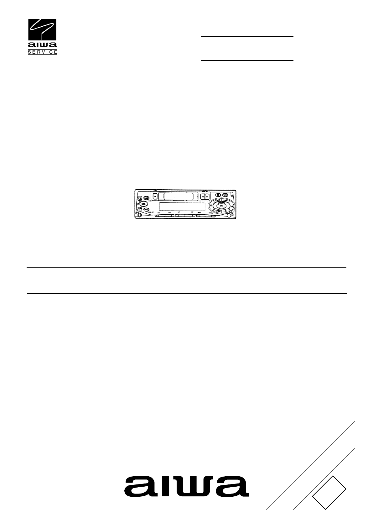
SERVICE MANUAL
STEREO CAR CASSETTE RECEIVER
This Service Manual is the "Revision Publishing" and replaces "Simple Manual"
(S/M Code No. 09-997-334-8T1).
BASIC TAPE MECHANISM : CDS-36SCH-94
S/M Code No. 09-997-334-8R1
REVISION
DATA
Page 2

SPECIFICATIONS
RADIO SECTION
(FM)
Frequency Range: 87.5 MHz–108 MHz
(100-kHz steps)
87.5 MHz-108 MHz
(50-kHz steps)
Usable Sensitivity: 12.7 dBf
50 dB Quieting Sensitivity: 17.2 dBf
IF Rejection: 80 dB
Frequency Response: 30 Hz-15,000 Hz
S/N Ratio: 63 dB
Stereo Separation: 35 dB at 1 kHz
Alternate Channel Selectivity: 70 dB
Capture Ratio: 3 dB
(AM(MW))
Frequency Range: 530 kHz–1,710 kHz
(10-kHz steps)
522 kHz–1,602 kHz
(9-kHz steps)
Usable Sensitivity: 30 µV (30 dB)
TAPE SECTION
Tape Speed: 4.8 cm/sec. (17/8 ips)
S/N Ratio: 50 dB
Frequency Response: 40 Hz–14,000 Hz
Stereo Separation: 40 dB
FF/REW Time: 190 sec. (C-60)
AUDIO SECTION
Max. Power Output: 40 W ×4 channels
CD/MD IN input
Input sensitivity (load impedance)
CD/MD IN: 500mV (10 kΩ)
GENERAL
Power-Supply Voltage: 14.4 V (11 to 16 V allowable),
DC, negative ground
Load Impedance: 4Ω
Tone Control: Bass ±10 dB at 100 Hz
Treble ± 10 dB at 10 kHz
Preamp Output Voltage (load impedance):
2.2 V (10 kΩ)
Installation size: 182(W) ×53(H)×155(D) mm
1
(7
/4(W)×21/8(H)×61/8(D) inches)
ACCESSORIES LIST
• Design and specifications are subject to change without notice.
REF. NO PART NO. KANRI DESCRIPTION
1 8Z-KTG-905-010 IB,YL(3L) 4019/4059
2 8Z-KTG-906-010 IB,INST,YL (3L)4019/4059
3 86-KT1-237-010 HLDR,REAR MTG
4 87-B10-141-010 NUT,5 TYPE-2
5 87-B10-143-010 UT1+5-15 W/O SLOT
6 87-B10-144-010 W,5.2-10-0.5
7 87-B10-145-010 W-SPR,5.3-8.5-1.5
8 88-KT1-247-010 S-SCREW,HEXAGON
9 8Z-KT1-231-010 HLDR,HALF -T
10 8Z-KT1-232-010 KEY,REMOVE -T *
NO.
REF. NO PART NO. KANRI DESCRIPTION
11 8Z-KT1-251-010 S-SCREW,5*6 TH+ TAPPING ST
12 8Z-KT1-616-010 CONN ASSY,16P B52
13 8Z-KT1-030-010 CASE,DFP -T
14 8Z-KTG-951-010 SPKR,16CM ASSY<4059>
15 88-KT1-250-010 S-SCREW,THIN HEAD+2.6-4 BLK
NO.
2
Page 3

ELECTRICAL MAIN PARTS LIST
REF. NO PART NO. KANRI DESCRIPTION
IC
8Z-KT1-622-010 C-IC,LC75374E
8Z-KTG-622-010 IC,TA8259H
8Z-KTG-621-010 C-IC,TC9323F-007
88-KT1-606-080 IC,PST994D
88-KTD-602-010 C-IC,TC9297F
88-KTD-604-010 IC,BA09T
87-A21-191-010 IC,KIA6225S
TRANSISTOR
87-A30-287-040 C-TR,DTC114TKA
89-324-122-080 TR,2SC2412KR
87-A30-289-040 C-TR,2SA1037AK(R)
87-A30-281-040 C-TR,DTC363TK
8Z-KTH-626-080 TR,KTC3203Y
87-A30-168-010 TR,2SB1566F
89-423-953-010 TR,2SD2395F
87-A30-294-040 C-TR,DTB123YK
87-A30-282-040 C-TR,DTA114TKA
DIODE
87-A40-529-080 DIODE,1GWJ42
87-020-465-080 DIODE,1SS133 (110MA)
87-A40-654-010 DIODE,DSA17C
87-001-783-080 DIODE,1N4002
87-017-932-080 ZENER,MTZJ6.2B
87-070-334-080 ZENER,MTZJ10B
87-070-136-080 ZENER,MTZJ5.1B
87-020-585-080 CHIP-ZENER,02CZ6.2Y
MAIN C.B
ANT101 8Z-KT1-614-010 ANT,AW-002
C101 87-010-322-080 C-CAP,S 100P-50 CH
C102 87-010-186-080 CAP,CHIP 4700P
C103 87-010-380-010 CAP,E 47-16 SME
C104 87-010-380-010 CAP,E 47-16 SME
C105 87-010-322-080 C-CAP,S 100P-50 CH
C106 87-010-197-080 CAP, CHIP 0.01 DM
C109 87-010-197-080 CAP, CHIP 0.01 DM
C110 87-010-197-080 CAP, CHIP 0.01 DM
C111 87-010-401-010 CAP, ELECT 1-50V
C112 87-010-198-080 CAP, CHIP 0.022
C113 87-010-378-010 CAP, ELECT 10-16SME
C114 87-010-378-010 CAP, ELECT 10-16SME
C115 87-010-220-080 C-CAP,S 0.018-25 B
C116 87-010-220-080 C-CAP,S 0.018-25 B
C117 87-010-180-080 C-CER 1500P
C118 87-010-180-080 C-CER 1500P
C119 87-010-401-010 CAP, ELECT 1-50V
C120 87-010-401-010 CAP, ELECT 1-50V
C121 87-010-197-080 CAP, CHIP 0.01 DM
C122 87-010-197-080 CAP, CHIP 0.01 DM
C123 87-010-380-010 CAP,E 47-16 SME
C124 87-016-669-080 C-CAP,S 0.1-25 K B
C201 87-016-669-080 C-CAP,S 0.1-25 K B
C203 87-010-182-080 C-CAP,S 2200P-50 B
C204 87-010-198-080 CAP, CHIP 0.022
C205 87-010-263-010 CAP, ELECT 100-10V
C206 87-010-322-080 C-CAP,S 100P-50 CH
C207 87-010-112-010 CAP,ELECT 100-16V
C208 87-010-235-010 ELECTROLYTIC, 470-16
C209 87-010-248-010 CAP, ELECT 220-10V
C210 87-016-669-080 C-CAP,S 0.1-25 K B
C211 87-016-669-080 C-CAP,S 0.1-25 K B
C212 87-010-112-010 CAP,ELECT 100-16V
C213 87-010-380-010 CAP,E 47-16 SME
NO.
REF. NO PART NO. KANRI DESCRIPTION
C251 87-010-198-080 CAP, CHIP 0.022
C301 87-012-349-080 C-CAP,S 1000P-50 CH
C302 87-012-349-080 C-CAP,S 1000P-50 CH
C303 87-010-378-010 CAP, ELECT 10-16SME
C304 87-010-378-010 CAP, ELECT 10-16SME
C305 87-010-263-010 CAP, ELECT 100-10V
C306 87-010-263-010 CAP, ELECT 100-10V
C307 87-010-198-080 CAP, CHIP 0.022
C308 87-010-198-080 CAP, CHIP 0.022
C309 87-010-401-010 CAP, ELECT 1-50V
C310 87-010-401-010 CAP, ELECT 1-50V
C311 87-010-263-010 CAP, ELECT 100-10V
C401 87-010-380-010 CAP,E 47-16 SME
C402 87-016-669-080 C-CAP,S 0.1-25 K B
C403 87-010-378-010 CAP, ELECT 10-16SME
C404 87-010-378-010 CAP, ELECT 10-16SME
C405 87-010-401-010 CAP, ELECT 1-50V
C406 87-010-401-010 CAP, ELECT 1-50V
C407 87-010-184-080 CHIP CAPACITOR 3300P(K)
C408 87-010-184-080 CHIP CAPACITOR 3300P(K)
C409 87-010-198-080 CAP, CHIP 0.022
C410 87-010-198-080 CAP, CHIP 0.022
C411 87-010-378-010 CAP, ELECT 10-16SME
C412 87-010-378-010 CAP, ELECT 10-16SME
C413 87-A11-177-080 C-CAP,S 0.15-16 K B
C414 87-A11-177-080 C-CAP,S 0.15-16 K B
C415 87-A11-177-080 C-CAP,S 0.15-16 K B
C416 87-A11-177-080 C-CAP,S 0.15-16 K B
C417 87-010-378-010 CAP, ELECT 10-16SME
C418 87-010-378-010 CAP, ELECT 10-16SME
C419 87-010-401-010 CAP, ELECT 1-50V
C420 87-010-401-010 CAP, ELECT 1-50V
C421 87-010-401-010 CAP, ELECT 1-50V
C422 87-010-401-010 CAP, ELECT 1-50V
C423 87-016-669-080 C-CAP,S 0.1-25 K B
C424 87-010-378-010 CAP, ELECT 10-16SME
C451 87-010-401-010 CAP, ELECT 1-50V
C452 87-010-401-010 CAP, ELECT 1-50V
C501 87-010-378-010 CAP, ELECT 10-16SME
C502 87-010-378-010 CAP, ELECT 10-16SME
C503 87-010-378-010 CAP, ELECT 10-16SME
C504 87-010-378-010 CAP, ELECT 10-16SME
C505 87-010-175-080 CAP 560P
C506 87-010-175-080 CAP 560P
C507 87-010-175-080 CAP 560P
C508 87-010-175-080 CAP 560P
C509 87-010-322-080 C-CAP,S 100P-50 CH
C601 87-016-669-080 C-CAP,S 0.1-25 K B
C602 87-016-669-080 C-CAP,S 0.1-25 K B
C603 87-016-669-080 C-CAP,S 0.1-25 K B
C604 87-016-669-080 C-CAP,S 0.1-25 K B
C605 87-016-669-080 C-CAP,S 0.1-25 K B
C606 87-016-669-080 C-CAP,S 0.1-25 K B
C607 87-A11-179-010 CAP,E 10-16-105 D5*L11 KMF
C608 8Z-KT1-633-000 CAP,E 3300U-16 105 PW
C609 87-012-157-080 C-CAP,S 330P-50 CH
C610 87-012-157-080 C-CAP,S 330P-50 CH
C611 87-012-157-080 C-CAP,S 330P-50 CH
C612 87-012-157-080 C-CAP,S 330P-50 CH
C621 87-010-182-080 C-CAP,S 2200P-50 B
C622 87-010-182-080 C-CAP,S 2200P-50 B
C623 87-016-669-080 C-CAP,S 0.1-25 K B
C701 87-010-380-010 CAP,E 47-16 SME
C702 87-010-263-010 CAP, ELECT 100-10V
C703 87-010-198-080 CAP, CHIP 0.022
C705 87-010-314-080 C-CAP,S 22P-50V
C706 87-010-197-080 CAP, CHIP 0.01 DM
C707 87-010-314-080 C-CAP,S 22P-50V
C708 87-010-314-080 C-CAP,S 22P-50V
C709 87-012-358-080 C-CAP,S 0.47-10 F Z
NO.
3
Page 4
REF. NO PART NO. KANRI DESCRIPTION
C710 87-010-401-010 CAP, ELECT 1-50V
C711 87-010-404-010 CONDENSER 4.7-50
C712 87-012-349-080 C-CAP,S 1000P-50 CH
C801 87-010-197-080 CAP, CHIP 0.01 DM
CN201 8Z-KT1-611-010 CONN,16P CAM-B51
CN301 87-009-031-010 CONNECTOR, 3P
CN302 87-099-408-010 CONN,8P EH V WHT
CN801 88-KTA-603-010 CONN,15P CAM-B68
CNA301 8Z-KTG-651-010 CONN ASSY,3P HEAD
CNA302 8Z-KTG-652-010 CONN ASSY,8P MOTOR
D806 87-027-262-010 LEDE,TLR-124(RED)
!F201 8Z-KC1-621-010 FUSE,15A 32V
J501 88-KTA-604-010 JACK,PIN 4P V-TYPE
L101 87-003-143-080 COIL 4.7 UH
L102 8Z-KT1-619-010 COIL,68MH K7-D
L201 8Z-KT1-615-010 FLTR,AMORPHOUS -CHOKE
L701 87-003-149-080 COIL,47UH
L702 87-003-097-080 COIL,1UH
L801 87-003-149-080 COIL,47UH
S751 87-A91-152-010 SW,SL 1-1-2 SSSS212-11-A
TU101 8Z-KT1-631-010 TU UNIT, FAE347-A02
X701 87-A70-175-010 VIB,XTAL 4.5MHZ AT-49
FRONT C.B
C901 87-012-358-080 C-CAP,S 0.47-10 F Z
C902 87-010-197-080 CAP, CHIP 0.01 DM
C903 87-010-189-080 C-CAP,S 8200P-50 B
C904 87-010-189-080 C-CAP,S 8200P-50 B
C905 87-010-805-080 CAP, S 1-16
CN901 88-KTA-602-010 CONN,15P CAM-B67
IC902 87-A90-951-010 RCR UNIT,SBX1971-52
LCD901 8Z-KTG-606-010 LCD,ZKT-16
PL901 8Z-KTA-610-010 LAMP,T-3-9V-50MA
PL902 8Z-KTA-610-010 LAMP,T-3-9V-50MA
NO.
REF. NO PART NO. KANRI DESCRIPTION
PL903 8Z-KTA-610-010 LAMP,T-3-9V-50MA
PL904 8Z-KTA-610-010 LAMP,T-3-9V-50MA
PL905 8Z-KTA-610-010 LAMP,T-3-9V-50MA
PL906 8Z-KTA-610-010 LAMP,T-3-9V-50MA
PL907 8Z-KTA-610-010 LAMP,T-3-9V-50MA
S901 87-A91-159-010 SW,TACT SKHLAD
S902 87-A91-159-010 SW,TACT SKHLAD
S903 87-A91-159-010 SW,TACT SKHLAD
S904 87-A91-159-010 SW,TACT SKHLAD
S905 87-A91-159-010 SW,TACT SKHLAD
S906 87-A91-159-010 SW,TACT SKHLAD
S907 87-A91-159-010 SW,TACT SKHLAD
S908 87-A91-159-010 SW,TACT SKHLAD
S909 87-A91-159-010 SW,TACT SKHLAD
S910 87-A91-159-010 SW,TACT SKHLAD
S911 87-A91-159-010 SW,TACT SKHLAD
S912 87-A91-159-010 SW,TACT SKHLAD
S913 87-A91-159-010 SW,TACT SKHLAD
S914 87-A91-159-010 SW,TACT SKHLAD
S915 87-A91-159-010 SW,TACT SKHLAD
S916 87-A90-001-010 C-SW,TACT SKQMAL
S917 87-A90-001-010 C-SW,TACT SKQMAL
S918 87-A90-001-010 C-SW,TACT SKQMAL
S919 87-A90-001-010 C-SW,TACT SKQMAL
S920 87-A90-001-010 C-SW,TACT SKQMAL
S921 87-A90-001-010 C-SW,TACT SKQMAL
JACK C.B
J901 87-A60-249-010 JACK,MOJ-B32
HEAD C.B
SW C.B
NO.
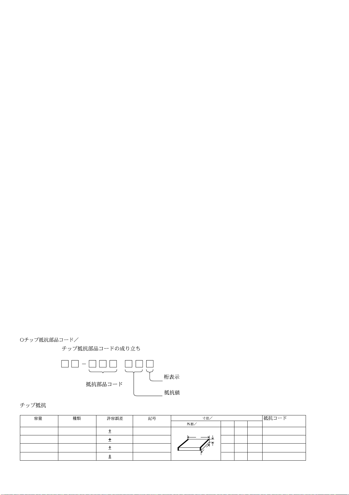
CHIP RESISTOR PART CODE
Chip Resistor Part Coding
88
A
Resistor Code
Chip resistor
Wattage Type Tolerance
1/16W 1005 5% CJ
1/16W
1/10W
1/8W
1608
2125
3216
5%
5%
5%
Symbol
CJ
CJ
CJ
Figure
Value of resistor
4
Form
L
W
Dimensions (mm)
LW t
1.0 0.5 0.35 104
t
1.6 0.8 0.45
2 1.25 0.45
1.6
0.55
3.2
Resistor Code
108
118
128
: A
: A
Page 5
TRANSISTOR ILLUSTRATION
E C B
KTC3203
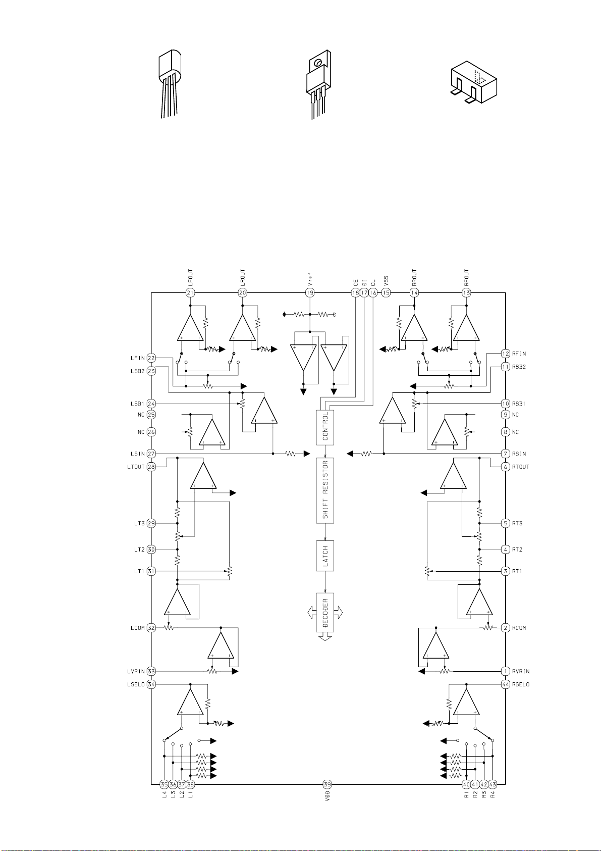
IC BLOCK DIAGRAMS
IC, LC75374E
B C E
2SB1566
2SD2395
C
B
E
2SA1037
2SC2412
DTA114TKA
DTB123YK
DTC1 14TKA
DTC363TK
5
Page 6
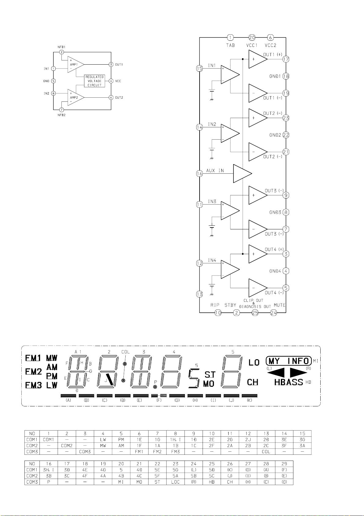
IC, KIA6225S IC, T A8259H
LCD DISPLAY
6
Page 7

BLOCK DIAGRAM
J501-1
(FRONT)
J501-2
(REAR)
87
Page 8

SCHEMATIC DIAGRAM-1 (MAIN/HEAD/SW SECTION)
4.5MHz
C501 10/16
C502 10/16
C504
C505 560p
C506 560p
FRONT
J501-1
J501-2
109
Page 9

WIRING-1 (MAIN/HEAD SW SECTION)
J501-2
REAR
J501-1
FRONT
C505
C506
1
A
B
C
234567
8
9
10
11 12 13
14
D
E
F
G
H
I
J
1211
Page 10

WIRING-2 (FRONT SECTION)
23456 654321
1
A
A
B
B
C
C
D
D
E
E
F
F
G
H
K
G
H
I
I
J
J
K
L
L
M
N
M
N
1413
Page 11

SCHEMATIC DIAGRAM-2 (FRONT SECTION)
15
Page 12

IC DESCRIPTION
IC, TC9323F
Pin No. Pin Name I/O Description
1 ~ 4
5
N.C
_______
APS
–
O
Not connected.
MS signal output
10
11
12
13
14
15
16
17
18
6
7
8
9
N.C
S-MUTE
______________
P-MUTE
LOUD
LOCAL
MONO
20dB MUTE
–
Not connected.
O
Standby muting output
O
Muting output to power amp
O
Loudness output
O
Local/DX switching output. LOCAL: "H", DX: "L"
O
MONO/STEREO switching output. MONO: "H", STEREO: "L"
-20dB muting output. This function is enabled when the -20dB muting jumper is
O
selected.
Outputs "H" during searching of frequency. This is an IF count control signal or used
AGC cut/IF REQ
O
to shut off the AGC circuit.
RADIO
TAPE
CD
O
O
O
RADIO output
TAPE output
CD output
Band switching outputs
BAND 1
O
BAND1 BAND2
FM H L
MW L L
BAND 2
O
LW L H
FM (L) H H
19 ~ 21
22 ~ 25
26 ~ 29
30 ~ 33
34 ~ 37
38 ~ 45
46
47
48
49
50 ~ 51
52
53
54
55
56
57
OT19 ~ OT21
P50 ~ P53
P60 ~ P63
P70 ~ P73
K0 ~ K3
DS0 ~ DS7
TAPE
CD
PANEL
POWER
NC
DIR
FF/REW
DATA
CK
CE
NC
O
Not connected
O
Not connected
O
Not connected
O
Not connected
I
Key matrix inputs
O
Diode matrix outputs
I
TAPE input
I
CD input. "H" CD input enables the CD key.
Detects detachable panel (0.2-0.5 s chattering time is provided). Panel provided: "H",
I
Panel not provided: "L"
O
Power output
O
Not connected
I
TAPE running direction indicator input
I
TAPE FF/REW indicator input
O
Pins to control the LC75374E electronic VR.
O
Not connected
58
LED FLASH
This function is enabled when the ACC input is "L" and PANEL input is "L". "H"
O
causes flashing for 0.1 s and "L" causes 0.9 s flashing. This output is disabled when the
LED FLASH jumper is "H".
16
Page 13

IC, TC9297F
Pin No. Pin Name I/O Description Pin No. Pin Name I/O Description
59
60
61
62
63
64
65
66
67
68
69
70, 71
72
73
74
75
76
77
78
79
80
DATA
CK
CE
BEEP
T-MUTE
REMO-IN
INTR 2
TEST
ACC IN
SD-IN
IF-IN
DO1, DO2
GND
FMIN
AMIN
VDD
_____________
RESET
XOUT
XIN
VXT
GND
I/O
O
O
O
O
O
–
–
O
–
–
For communications with LCD driver and key input IC TC9297F.
Buzzer output
I
Interrupt of remote control signal
I
I
Test mode control input
I
ACC input
I
SD signal input
I
IF signal input
DO outputs
GND
I
FM/AM local oscillator signal input
VDD terminal
I
Reset input
For the connection of a crystal oscillator
I
GND
1 ~ 4
5 ~ 10
11
12
13
14 ~ 48
49 ~ 52
53
54
55
56
K1 ~ K4
T0 ~ T5
COM1
COM2
S0/COM3
S1 ~ S35
______ _______
S36/OT3 ~ S39/OT0
GND
OSC
VDD
________
RST
Key scan inputs. A maximum of 6x5=30 key data can be input with a matrix of key
I
scan outputs T0 ~ T5. When "H" is applied to this pin, scanning of keys will start.
These pins incorporate pull-down resistors.
Key scan timing outputs. Since a load resistor RON is built into the N-ch to form a key
matrix, a diode is not necessary. In normal operation, these pins output "H", and when
O
"H" is applied to key scan inputs K0 ~ K4, key scanning will start.
O
LCD common signal outputs. When 1/2 duty is set, matrixing of COM1, 2 and
O
S0 ~ S39 allows the display of up to 80 segments. When 1/3 duty is set, matrixing of
COM1-3 and S1 ~ S39 allows display of up to 117 segments.In the 1/3 duty mode, the
O
S0 pin is used as a COM3 pin.
LCD segment signal outputs. When 1/2 duty is set, matrixing of COM1, 2 and
O
S0 ~ S39 allows display of up to 80 segments. When 1/3 duty is set, matrixing of
COM1-3 and S1 ~ S39 allows display of up to 117 segments. S36 ~ S39 are commonly
O
used for LED drivers. The LED driver outputs become N-ch open drain outputs, and
the LEDs can be directly indicated since they are driven by high current.
GND
–
C and R which are attached externally form an oscillator.
The oscillation frequency is shown by the following formula:
–
fosc ≒ 1.5/(C・R)[Hz]
For example, when C = 0.01 μF and R = 30 k Ω ,
fosc ≒ 5 kHz.
Power supply input. Normally, a voltage VRST ~ 5.5 V is applied. This pin is provided
–
with a power-on reset function: the system reset will function when power is turned on
or VDD is less than 3 V (standard).
Device system reset signal input. When RST input is "L", the oscillator will stop, all
internal data will be reset and the LCD output pins and key scan output pins will be
I
_______
fixed at "H". For normal operation, connect this pin to VDD, since the device
incorporates a power-on reset circuit.
57
58
59
60
CK
DATA
CE
K0
I/O
Serial interface pins. The device communicates the display data, key input data and the
I
data which controls these with the controller. When the CE pin is "L", data will not be
communicated. When it goes "H", data will be communicated between the DATA pin
and controller, synchronized with the clock signal input to the CK input pin. All these
I
pins have Schmitt input circuits.
Key scan input. A maximum of 6x5=30 key data can be input with a matrix of key
I
scan outputs T0 ~ T5. When "H" is applied to this pin, scanning of keys will start. This
pin incorporates a pull-down resistor.
1817
Page 14

MECHANICAL EXPLODED VIEW 1/1
6
7
1
8
2
9
3
4
10
11
5
12
14
17
E
15
A
18
19
20
32
16
45
23
21
33
22
CDS-36
SCH-94
CHAS, SIDE L-T
B
B
CHAS,FRONT-T10
B
41
A
42
B
A
39
A
38
B
G
43
B
PANEL HEAT-SINK-T
D
B
F
44
B
24
PHONE C.B
LCD
25
26
FRONT C.B
29
28
27
SH,LCD
30
29
28
29
31
C
A
C
A
34
35
36
A
13
37
G
40
B
MAIN C.B
B
A
CHAS, SIDER-T
B
2019
Page 15

MECHNICAL MAIN PARTS LIST 1/1
REF. NO PART NO. KANRI DESCRIPTION
1 8Z-KTG-009-010 WINDOW,LCD X4019 IR<4019>
1 8Z-KTG-004-010 WINDOW,LCD X4059 IR<4059>
2 8Z-KTB-002-010 RING,OVAL T -T
3 8Z-KTG-008-010 BTN,CD/MD IN -T
4 8Z-KTF-003-010 BTN,TETRA BALD -T
5 8Z-KT1-011-010 BTN,U/D -T
6 8Z-KT1-007-010 BTN,+/- -T
7 8Z-KTG-002-010 CABI,FRONT -T16
8 8Z-KT1-008-010 BTN,SEL -T
9 8Z-KT1-010-010 BTN,H-BASS -T
10 8Z-KTA-005-010 BTN,EJ -T10
11 8Z-KTG-006-010 BTN,PWR -T
12 8Z-KTA-226-010 SPR-C,EJECT
13 8Z-KT1-212-010 COVER, BOTTOM -T
14 8Z-KTA-213-010 LENS,L -T10
15 8Z-KT3-002-010 BTN,P.SET -T3
16 8Z-KTA-214-010 LENS,R -T10
17 8Z-KTA-007-010 BTN,REW -T10
18 8Z-KTA-006-010 BTN,FF -T10
19 8Z-KT5-019-010 BTN,M.INF -T
20 8Z-KT5-020-010 HLDR,M.INF -T
21 8Z-KTA-008-010 BTN,DETACH -T10
22 8Z-KTA-223-010 SPR-C,RELEASE -T10
23 8Z-KTG-007-010 BTN,TWIN T/M -T
24 8Z-KTA-012-010 CABI,TRIM -T10
25 8Z-KTA-210-010 HLDR,LCD -T10
26 8Z-KTG-212-010 LENS,LCD -T16
27 8Z-KTG-211-010 CASE,LCD LENS -T16
28 8Z-KTG-207-010 CAP,LAMP BLU B2*4 ALC
29 8Z-KTG-208-010 CAP,LAMP GRN G50 ALC
NO.
REF. NO PART NO. KANRI DESCRIPTION
NO.
30 8Z-KTA-002-010 CABI,REAR -T10
31 8Z-KTA-011-010 CABI,BASE -T10
32 8Z-KT1-244-010 SPR-T,DOOR Z
33 8Z-KT1-023-010 DOOR,CASS
34 8Z-KTA-204-010 LEVER,DEF HOOK -T10
35 8Z-KTA-221-010 SPR-C,DETACH LOCK-T10
36 8Z-KTA-222-010 SPR-T,DETACH LOCK-T10
37 8Z-KTA-203-010 LEVER,DFP LOCK -T10
38 8Z-KT4-201-010 COVER, CD BLIND -T
39 8Z-KT1-265-010 HLDR,TR2
40 8Z-KTG-202-010 HLDR,P-IC -T16
41 8Z-KTA-202-010 HLDR,DECK CDS36
42 8Z-KT1-211-010 COVER, TOP -T
43 8Z-KT5-201-010 COVER, ISO BLIND -T
44 8Z-KT1-220-010 HLDR,JACK F -T
45 87-KTE-205-010 SPR-C,EJ/FF/REW
A 88-KT1-250-010 S-SCREW,THIN HEAD+2.6-4 BLK
B 87-251-073-410 SCREW,U+2.6-6
C 8Z-KT1-253-010 S-SCREW,PT 2*8 BH+ BLK
D 87-251-096-410 U+3-10
E 8Z-KT1-254-010 S-SCREW,PT 2*5 BH+ BLK
F 87-B10-210-010 UT2+3.0-6.0 W/0 SLOT (BH TAP)
G 87-251-075-410 U+2.6-10
COLOR NAME TABLE
Basic color symbol Color Basic color symbol Color Basic color symbol Color
B Black C Cream D Orange
G Green H Gray L Blue
LT Transparent Blue N Gold P Pink
R Red S Silver ST Titan Silver
T Brown V Violet W White
WT Transparent White Y Yellow YT Transparent Yellow
LM Metallic Blue LL Light Blue GT Transparent Green
LD Dark Blue DT Transparent Orange
21
Page 16

TAPE MECHANISM EXPLODED VIEW 1/1
28
25
29
32
D
49
U
P
D
69
59
C
55
56
60
61
A
62
M
54
46
47
R
N
81
48
52
A
53
57
D
B
H
68
67
66
80
Q
54
58
63
64
65
I
R
N
E
B
H
68
85
27
26
21
42
35
34
77
41
40
39
38
37
36
L
F
22
J
33
O
K
C
31
30
24
23
43
44
45
A
50
51
E
20
8
5
4
3
2
9
19
10
F
7
6
C
1
K
K
11
12
18
F
13
G
14
C
15
16
K
T
G
14
15
T
16
72
S
71
S
73
17
70
83
F
84
V
74
79
78
K
82
V
75
76
22
Page 17

TAPE MECHANISM PARTS LIST 1/1
REF. NO PART NO. KANRI DESCRIPTION
1 SX-003-610-090 REEL BASE ASSY
2 S0-036-201-000 GEAR SELECTOR
3 S1-003-630-180 COLLAR(SELECTOR GEAR)
4 S1-003-640-150 DASH SPG
5 S1-003-840-140 RATCHET SPG
6 S1-003-640-030 ARM SPG GEAR LOCK
7 S1-003-820-140 ARM GEAR LOCK
8 S1-003-620-070 RATCHET
9 S1-003-620-030 GEAR REDUCTION(B)
10 S1-003-620-010 GEAR,IDLE
11 S1-003-620-090 ARM SENSOR
12 S1-003-620-040 GEAR REDUCTION(A)
13 S1-003-620-140 GEAR DETECTOR
14 SX-003-660-810 REEL SPINDLE ASSY(D)
15 SX-013-620-010 DETECTOR CAM ASSY
16 S1-013-840-010 BACK TENSION SPG
17 S1-003-610-160 LEVER CONVERSION
18 S1-003-650-180 BELT SUB(C)
19 S1-003-620-050 GEAR PULLEY
20 SX-003-610-010 MAIN CHASSIS ASSY
21 S1-003-610-060 CAM,EJECT
22 S1-003-640-050 EJECT CAM SPG
23 S1-003-610-070 LEVER EJECT
24 S1-003-640-040 EJECT LEVER SPG
25 S1-013-810-100 HOLDER,CASS(X)
26 SX-003-610-190 EJECT CAM LOCK ASSY
27 S1-005-820-040 TAPE HOOKER
28 S1-013-810-020 HANGER CASS(X)
29 S1-003-640-070 EJECT CAM LOCK SPG
30 S1-003-640-230 CENTER PLATE SPG(B)
31 S1-003-610-180 PLATE CENTER
32 S1-003-650-060 LINK RETURN
33 S1-003-670-340 SW,POWER
34 S1-003-820-340 ARM MUTE(N)
35 S1-003-830-150 COLLAR ARM MUTE
36 S1-003-630-020 ROLLER HP(A)
37 S1-003-630-240 ROLLER HP(B)
38 SX-003-660-820 HEAD PLATE ASSY(S)
39 S1-003-640-130 PINCH ARM SPG(R)
40 S1-013-860-020 PINCH ARM(R) ASSY
41 S1-003-630-420 MOTOR PULLEY(MBC)
42 S1-003-670-570 MOTOR
43 S1-003-630-040 ROLLER FF
44 S1-003-610-150 SPG SUPPORT PLATE
45 S1-003-640-110 ADJUSTER ARM SPG(B)
46 S0-036-401-000 ADJUSTER ARM SPG(A)
47 S1-003-670-840 HEAD
48 S1-013-820-053 ARM ADJUSTER(B)
49 S1-013-810-060 ADJUSTER SHIM(X)
50 S1-003-820-180 GUIDE TAPE
51 S1-013-820-040 LINK ADJUSTER(X)
52 S1-013-860-030 PINCH ARM(L) ASSY
53 S1-003-640-120 PINCH ARM SPG(F)
54 S1-003-640-010 LEVER SPG FF/REW
55 S1-003-610-510 LEVER FF(AT)
NO.
REF. NO PART NO. KANRI DESCRIPTION
56 S1-003-610-530 LEVER REW(AT)
57 S1-003-640-060 HEAD PLATE SPG
58 S1-003-830-120 ROLLER PROGRAM
59 S1-003-610-230 LEVER,CHANGE(B)
60 S1-003-640-020 LEVER SPG LOCK
61 S1-003-610-290 LOCK ARM(A)
62 SX-003-660-770 LEVER BRACKET ASSY(D)
63 S1-003-640-080 PROGRAM ARM SPG
64 S1-003-640-170 CHANGING ARM SPG
65 S1-003-850-010 SELECTOR LINK(B)
66 SX-003-610-100 FR CHANGING ARM ASSY
67 SX-013-820-060 CM BRACKET ASSY(X)
68 S1-003-640-180 EARTH SPG(R)
69 SX-003-620-150 TU GEAR ARM ASSY
70 S1-005-820-215 PULLEY IDLE(A)
71 SX-003-610-250 FR ARM(A) ASSY
72 S1-003-620-080 ARM,FF
73 S1-003-610-260 ARM,FR(B)
74 S1-003-660-101 FLYWHEEL ASSY(BR)
75 S0-036-601-000 FLYWHEEL ASSY(BF)
76 S1-003-650-040 BELT MAIN
77 S1-001-250-170 MYLAR WASHER
78 S1-003-670-010 SW,PWB
79 S1-003-670-070 SW,SLIDE
80 S1-013-870-020 MUTE PWB
81 S1-013-870-870 SW,MUTE
82 S1-003-670-020 WIRE A 60MM(BLK)
83 S1-003-670-040 WIRE C 55MM(YEL)
84 S1-003-670-030 WIRE B 60MM(RED)
85 SX-003-660-750 MOTOR ASSY
A S2-171-150-401 E-RING 1.5
B S2-171-160-329 E-RING 1.6-3.2
C S2-171-200-501 E-RING 2.0
D S2-171-250-601 E-RING 2.5
E S2-133-170-30C SCREW,M1.7-3
F S2-181-200-30D PSW-S 1.2-3.0-0.25
G S1-003-650-230 PSW-S(REEL) 1.5-3.2-0.2
H S2-182-100-32D PSW 2.1-3.2-0.25
I S2-133-170-40C SCREW,M1.7-4
J S2-133-170-60C SCREW,M1.7-6
K S2-138-200-30C SCREW,M2-3
L S2-136-200-40F SCREW,FLAT M2-4
M S2-133-200-40C SCREW,PLAIN M2-4
N S2-103-200-70C SCREW,PLAIN M2-7
O S2-103-200-25C SCREW,PLAIN M2-2.5
P S2-101-200-40C SCREW,PLAIN M2-4
Q S2-101-200-30F SCREW,FLAT M2-3
R S1-013-850-020 SCREW,AZIMUTH PLAIN M2-5
S S1-003-650-050 SCREW,HOOK EJECT M2-5
T S1-013-650-010 LMW(REW)2.1-3.5-0.05
U S1-003-650-240 PSW B(REEL) 1.5-3.2-0.25
V S1-003-650-280 LMW(FLY)2.1-5.5-0.05
NO.
23
Page 18

2–11, IKENOHATA 1–CHOME, TAITO-KU, TOKYO 110-8710, JAPAN TEL:03 (3827) 3111
737004
Printed in Singapore
 Loading...