

Page 1
a n u a
SER VI CE
CT-X2058
CT-X2018
REVISION PUBLISHING
This Service Manual is the "Revision Publishing" and replaces "Simple Manual"
(S/M Code No. 09-983-263-401).
S/M Code No. 09-9 84 -26 0- 60 1
SERVICE MANUAL
Page 2

SPECIFICATIONS
RADIO SECTION
(FM)
Frequency Range:
Usable Sensitivity:
50 dB Quieting Sensitivity:
IF Rejection:
Frequency Response:
S/N Ratio:
Stereo Separation:
Alternate Channel Selectivity:
Capture Ratio:
(AM)
Frequency Range:
Usable Sensitivity:
TAPE SECTION
Wow/Flutter:
Tape Speed:
S/N Ratio:
Frequency Response:
Stereo Separation:
FF/REW Time:
87.5 MHz-108 MHz
(100-kHz steps)
87.5 MHz-108 MHz
(50-kHz steps)
12.7 dBf
17.2 dBf
80 dB
30 Hz-15,000 Hz
63 dB
35 dB at 1 kHz
70 dB
3 dB
530 kHz-1,710 kHz
(10-kHz steps)
522 kHz-1,620 kHz
(9-kHz steps)
30 pV (30 dB)
0.1% (WRMS)
4.8 cm/sec. {Vk ips)
50 dB
40 Hz-14,000 Hz
40 dB
190 sec. (C-60)
AUDIO SECTION
Max. Power Output: 25 W X 4 channels
CD IN input
Input sensitivity (load impedance)
CD IN: 500mV (10 k Q )
GENERAL
Power-Supply Voltage: 14.4 V (11 to 16 V allowable),
DC, negative ground
Load Impedance: 4 Q
Tone Control: Bass ± 10 dB at 100 Hz
Treble ± 10 dB at 10 kHz
Preamp Output Voltage (load impedance):
2.2 V (10k Q )
Installation size: 182(W) X 53(H) X 155(D) mm
(774(W) X 21/s(H) X 6Ve(D) inches)
> Design and specifications are subject to change without
notice.
ACCESSORIES LIST
DESCRIPTIONTIffTcT& "REFERENCE NAME LIST" $ # i b T < tz S l>0
If can't understand for Description please kindly refer to "REFERENCE NAME LIST"
REF. NO PART NO. KANRI DESCRIPTION
1 S7-0X8-147-001
2 S2-2X8-KT2-000
3 S2-2X5-KT4-000
SO-9X6-KT1-OOC) PANEL CASE P.P
4
5 S2-050-654-091 NUT M5
6 Sl-850-031-520 SCREW,5-15
SO — 650 —651 —014 SCREW,10-M5-10
7
8 S3-309-005-203
S3-410-005-003 PLANE WASHER 10-5-0.5
9
10 S6-694-326-2ES
NO.
IB ENG/SPA/P0RTU
KEY,RELEASE
REAR MOUNTING BRACKET
SPRING WASHER M5
SPK
2
Page 3

ELECTRICAL MAIN PARTS LIST
D ES C RIP TIO N T fllfrT^& ^tl« "REFERENCE NAME LIST"
If can't understand for Description please kindly refer to "REFERENCE NAME LIST".
REF. NO PART NO. KANRI DESCRIPTION REF. NO PART NO. KANRI DESCRIPTION
S3-320-622-564 IC,KIA6225S
S3-375-373-E16 IC,LC75373E
87-A20-599-010
S3-350-994-D84 IC, PST994D
S3-32B-A09-T18
87-A20-877-010
S3-339-297-F14
TRANSISTOR
87-026-464-080
87-026-610-080
S1-71H-003-EOO
87-026-311-080
S3-147-320-325
S3-1KT-A16-58Y
S3-1KT-C43-69Y TR,KTC4369Y
87-026-572-080 TR,DTA114TS
S3-1DT-C36-3TS TR,DTC363TS
DIODE
87-020-465-080 DIODE,1SS133VR=35V
87-001-783-080 DIODE, 1N4002
87-070-334-010 ZENER,
87-070-136-080 ZENER, 5. IV
87-017-932-080
S3-040-806-2UD C-ZENER,DIODE (SMD TYPE)
87-017-779-080 DIODE,1SS355
MAIN C.B
C105
C107
C108 87-010-553-080
C109
C110 87-010-053-080
C115 87-010-053-080
C116
C118
C203
C204
C205 87-010-555-010
C206
C209
C210 87-010-053-080
C211
C231 87-010-553-080
C301 87-010-553-080
C303 87-010-053-080
C304
C305
C306
C311
C312
C317
C318 87-010-378-040
C319 87-010-053-080 CAP, E
C320
C321
C322
C324
C457
C458 87-010-053-080
C501 87-010-053-080
C502
C503 87-010-053-080 CAP, E
C504
87-010-553-080
87-010-495-040 CAP, E 2.2-50V
87-010-053-080
87-010-053-080 CAP, E
87-010-553-080
87-010-378-040
87-010-378-040
87-010-555-010
87-010-053-080
87-010-555-010 CAP, E
87-010-053-080 CAP, E 1-50V
87-010-378-040 CAP, E
87-010-378-040
87-010-378-040
87-010-378-040
87-010-378-040
87-010-053-080 CAP, E
87-010-053-080
87-010-053-080 CAP, E
87-010-553-080 CAP, E 47-16V
87-010-053-080
87-010-053-080
87-010-053-080 CAP, E
NO. NO.
IC,HA13154A
IC,BA09T
IC,TC9321F-015
IC,TC9297F
TR,DTC114TS
TR,KTC3198-Y
TR,KTA1267Y
TR,DTB123YS
TR,KTC3203Y
TR,KTA1658Y
MTZ10B
ZENER,MTZJ6.2B
CAP, E 47-16V
CAP,E
47-16V
CAP,E 1-50V
CAP,E
1-50V
CAP, E 1-50V
1-50V
CAP, E 47-16V
CAP, E
10-16V
CAP,E
10-16V
CAP,E
100-10V
CAP,E
100-10V
CAP,E 1-50V
CAP,E
1-50V
100-10V
CAP,E 47-16V
CAP,E
47-16V
CAP,E
1-50V
10-16V
CAP, E
10-16V
CAP, E 10-16V
CAP, E
10-16V
CAP,E
10-16V
CAP, E
10-16V
1-50V
1-50V
CAP, E 1-50V
1-50V
CAP, E
1-50V
CAP,E
1-50V
CAP, E
1-50V
CAP, E 1-50V
1-50V
1-50V
C509 87-010-866-010 CAP, E 10UF-63V
C510
C602 87-015-682-040 CAP, E 22-16V
C603 87-010-248-040
C604 87-010-112-040
C605 87-010-553-080 CAP, E
C606 87-010-555-010
C633 87-010-553-080 CAP, E 47-16V
C702 87-010-555-010 CAP, E 100-10V
C751
C752 87-015-698-080 CAP,E 4.7-50V
C753
C831
C832 87-010-053-080 CAP,E 1-50V
CON231
CON831 S6-051-5B6-8M1 CONN, 15P DET
D701
J101
J451 S6-1DA-E24-2V5 JACK,RCA 2P
L101 87-003-143-080 COIL,4.7UH 2X4MM
L701
L702
L731
SW901
TUN101 SO-3FA-E34-001
X701
FRONT C.B
CON801 S6-051-5B6-7M1 CONN,15P DET
LCD801
PL801 S3-6X8-KT1-006
PL801
PL802 S3-6X8-KT1-006 LAMP CAP BLUE
PL802 S8-790-653-602 PILOT LAMP 9V 60MA
PL803 S3-6X6-KT1-000 LAMP CAP GREEN
PL803
PL804 S3-6X6-KT1-000 LAMP CAP GREEN
PL804 S8-790-653-602 PILOT LAMP 9V 60MA
PL806
PL806
PL807 S3-6X6-KT1-000 LAMP CAP GREEN
PL807
PL808
PL808
SW801
SW802
SW803
SW804
SW805
SW806
SW807
SW808
SW809
SW810 S4-711-0S5-0K1
SW811
SW812
SW813 S4-711-0S5-0K1 SW,SMD TACT 2 PIN
SW814
SW815
SW816
SW817 S4-711-015-OK1 SW, TACT 2PINS
SW818
SW819
SW820
JACK C.B
87-010-377-010 CAP, E
87-010-553-080 CAP, E
87-010-053-080 CAP,E 1-50V
87-010-053-080 CAP,E 1-5 0V
S6-040-825-5NT CONN,8P 2.5 PITCH WAFER
S3 — 051-012—400 LED,LAMP 3MM(RED)
S8-48K-T67-900 ANT,SOCKET
87-003-149-080 COIL,47UH
87-003-383-010
87-003-149-080 COIL,47UH
S4-1SK-Y12-002 SW,SLIDE MINI 1P2T
S3-772-000-013 X' TAL,7.2 MHZ
S3-580-08K-TKA LCD,DISPLAY
S8-790-653-602 PILOT LAMP 9V 60MA
S8-790-653-602 PILOT LAMP 9V 60MA
S3-6X6-KT1-000 LAMP CAP GREEN
S8-790-653-602
S8-790-653-602
S3-6X6-KT1-000 LAMP CAP GREEN
S8-790-653-602
S4-711-015-0K1
S4-711-015-0K1
S4-711-015-0K1
S4-711-015-0K1
S4-711-015-0K1
S4-711-015-0K1
S4-711-015-0K1
S4-711-015-0K1
S4-711-015-0K1 SW, TACT 2PINS
S4-711-0S5-0K1
S4-7U-015-0K1
S4-711-015-0K1
S4-711-015-0K1
S4-711-015-0K1
S4-711-015-OK1
S4-711-015-OK1
S4-711-015-0K1
3300UF-16V
CAP, E
220-10V
CAP, E
100-16V
47-16V
CAP, E
100-10V
47-16V
COIL,1UH
TUNER PACK FAE340-A02
LAMP CAP BLUE
PILOT LAMP 9V 60MA
PILOT LAMP 9V 60MA
PILOT LAMP 9V 60MA
SW, TACT 2PINS
SW, TACT 2PINS
SW, TACT 2PINS
SW, TACT 2PINS
SW, TACT 2PINS
SW, TACT 2PINS
SW, TACT 2PINS
SW, TACT 2PINS
SW, SMD TACT 2PIN
SW, SMD TACT 2 PIN
SW,TACT 2PINS
SW, TACT 2PINS
SW, TACT 2PINS
SW, TACT 2PINS
SW,TACT 2PINS
SW, TACT 2PINS
SW, TACT 2PINS
3
Page 4

REF.NO PART NO. . KANRI DESCRIPTION
J801 S6-1MO-JB3-2BO JACK,AUX
HEAD C.B
SW C.B
O f 7 3 — F / CHIP RE SIST O R PART CO DE
NO.
9 y n - F © f£ 9 Ï l%
Chip Resistor Part Coding
3 E - □ □ □ □ □ □
A
Resistor Code
9 " j y ° W s K
Chip resistor
mm
Wattage
1/16W
1/10W
1/8W
TRANSISTOR ILLUSTRATION
Type
16 0 8
212 5
321 6 5 %
Tolerance
5%
5%
im
Symbol
CJ
CJ
CJ
Figure
m Kffi
Value of resistor
¿
I
-----
\f"S; / Diamensions (mm)
/ Form
L
1. 6 0.8
2 1.2 5 0.45
3.2 1. 6 0.55
t Resistor Code : A
W
0.45
f i Jn n - F : A
10 8
118
128
EC B
KTC3198
KTC3203
w
EC B
DTA114TS
DTB123YS
DTC114TS
DTC363TS
KTA1267
4
$
BCE
KTA1658
KTC4369
Page 5

BLOCK DIAGRAM
5
6
Page 6

WIRING-1
1
B
C
(MAIN SECTION)
2 |
TO ANTENN A
J 1 0 1
S S S S
"S»+
P k o 4
’m R2 0 3
y\ •A A A /- *
_______
3 |
_______
• a a / v #
W a f r
4 [
_______
5 |
_______
6 j 7 j 8 I 9 | 10 [ 11 | 12 | 13 | 14
---
R ( - )
R ( + )
L ( - >
L (+ )
V L T / B L O
— < V LT >
G RN / B LK >
—<GRN>
---
---
tiPNfcO 1
<GRY>—
< G RY /B LK
---
<WHT >—
< W H T/ B LK
•R (+)
•R (-)
-L (+)
•L (-)
TO
FRO N T
SP E A K E R
C < E S P
D
R751 tr
E
► V W «
07 55 Q 7 5 6 07 54 Q753
l \ m » m
■ . . . mmrnjmSm 6
•-'WV»
SW 3
(F F/ R EW )
SW 2 M1
(PA C K -IN ) (R E E L MOTOR)
F
C, 60 7
G
SW90 1
Q 1 0 4
• A A V »
PH4£ "
•wyVV»
ß
HEA-B C. B
-<GRY>-
-< VLT> -
SW 1
(F /R )
H
• A A A r *
r i 1 a
»AAV«
E Z jO Z
C 3 -
r a -
-<YEL>—I
-<REB>—
-<WHT>
-<PNK>
-<BLK>
-<BLK>
C 0 N 8 3 1
J
co
' X T ?
V h- V
Z I _l
CL > PQ
Y Y Y,
C0€I20 1
Page 7
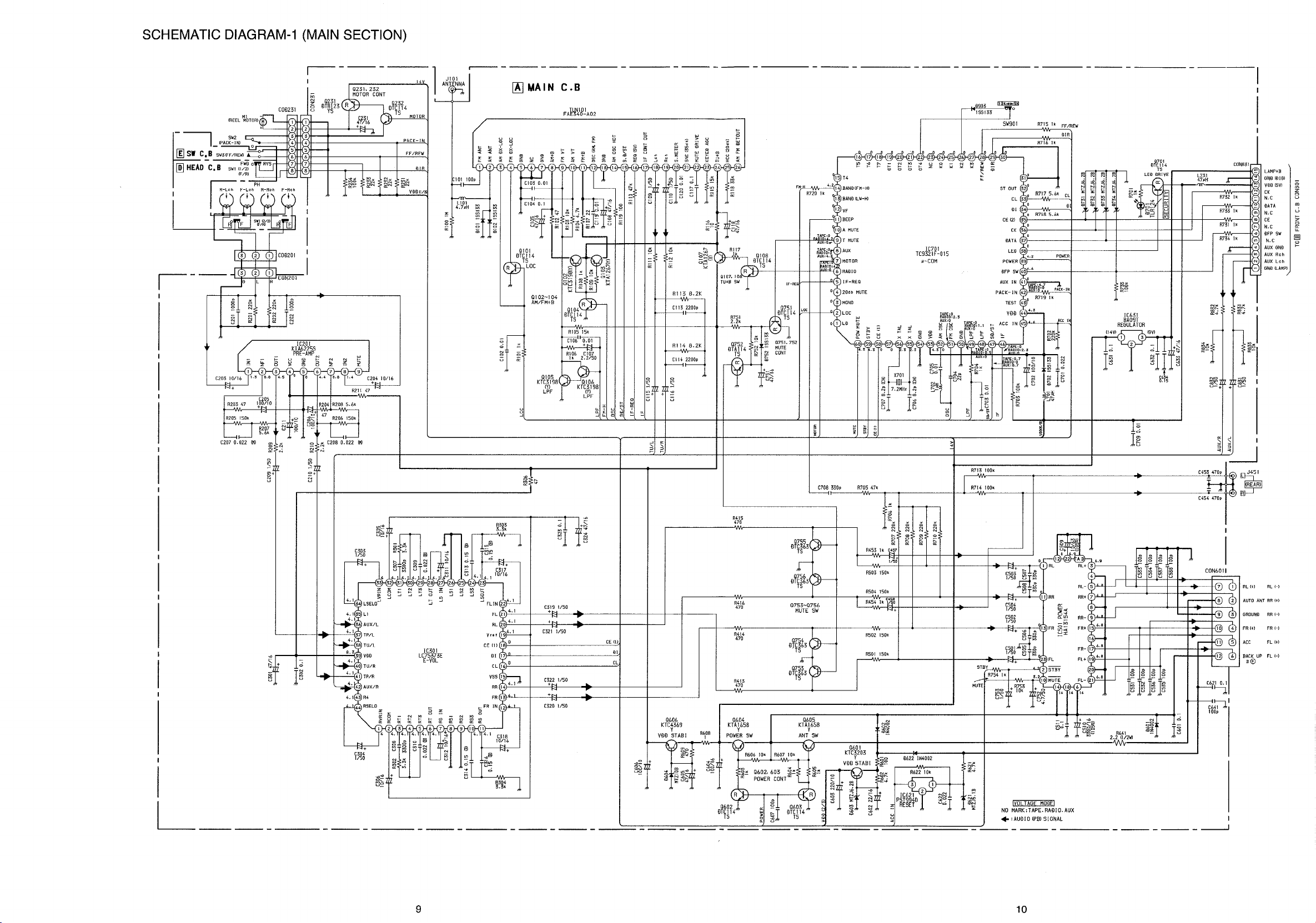
SCHEMATIC DIAGRAM-1 (MAIN SECTION)
9
10
Page 8

WIRING-2 (FRONT SECTION)
B FRONT C. B
BJ FRON! C. B
SW807 |W814
TUNEAl ICRPl
5WS20 5W809
ICS INI iBANfll
SW!! 1 0 SW81
1X7 'TeI I LO
SW81
E H]
ISW808
| W 8 0 1
m
PLf i0 1 ~804, E 0 6-8 08
( I LLUM I NAT I ON)
CJ JACK
C. B
J80 1
fl I Nl
r
L
11
SW81 9
I MUTE I
SW81 7SW8 1 8
SW8 1 2
IH- BASS I
12
Page 9

TO 0 MAIN C .B C0N831
SCHEMATIC DIAGRAM-2 (FRONT SECTION)
B FRONT C.B
© i © ?
m m
5W0O3n
a
TU N ET
CO
SW8I3
SW8I7
0
a.
n
a
P L 8 0 K 804 , 8 0 6 ^ 8 0 8
PIL O T LAMP 9V 60MA
(ILL UM INA TIO N)
©s © ~
SW804 @ SW805
SW809 5W8IQ
[ÄTmeI
a
5W818
□
a
© z
M ' i in - f l N C O ff l - - - -- - - -
(nuiintntocncncntntntncncncnin
0-NNlvfm>OS
FM123 m f
MW AM ,J -'
7 i t ? n
H BASS CRP
LW PM 1-Ul-zfJJrLLJÜ .“ ° 8 i? ir
LCBB01 (BI SPLAY)
Page 10

1C DESCRIPTION
1C, TC9297F
Pin No.
1 -4
5-1 0 T0- T 5
1 1
12
13
14-48 SI ~ S35
49 -52
53 GN D
54
Pin Name
K1 - K4 I
COM1 O
COM 2
SO/COM3 O
S36/OT3 - S39/OTO
OSC
I/O Description
Key scan inputs. A maximum of 6x5=30 key data can be input with a matrix of key
scan outputs TO - T5. When "H " is applied to this pin, scanning o f keys w ill start.
These pins incorporate pull-down resistors.
Ke y scan timing outputs. Since a load resistor RO N is built into the N-ch to form a key
0
matrix, a diode is not necessary. In normal operation, these pins output "H ", and when
"H " is applied to key scan inputs K0 ~ K4, key scanning w ill start.
LC D common signal outputs. When 1 /2 duty is set, matrixing o f CO M1, 2 and
O
SO - S39 allows the display of up to 80 segments. When 1/ 3 duty is set, matrixing of
COM1-3 and S I ~ S39 allows display of up to 117 segments.In the 1/ 3 duty mode, the
SO pin is used as a COM 3 pin.
LC D segment signal outputs. When 1/ 2 duty is set, matrixing of COM 1, 2 and
o
SO - S39 allows display of up to 80 segments. When 1/ 3 duty is set, matrixing of
COM1-3 and S I - S39 allows display of up to 117 segments. S36 - S39 are commonly
0
used for L ED drivers. The LED driver outputs become N-ch open drain outputs, and
the L ED s can be directly indicated since they are driven by high current.
—
—
GN D
C and R which are attached externally form an oscillator.
The oscillation frequency is shown by the follow ing formula:
fosc = 1.5/(C • R)[H z]
For example, when C = 0.01 ¡x F and R = 30 k fl ,
fosc = ? 5 kHz.
55 VD D
56 RST
57 C K
58 D AT A
59 C E I
60
K0
I/O
Power supply input. Normally, a voltage V R ST - 5.5 V is applied. This pin is provided
with a power-on reset function: the system reset w ill function when power is turned on
or V DD is less than 3 V (standard).
Device system reset signal input. When R ST input is "L", the oscillator w ill stop, all
internal data w ill be reset and the LCD output pins and key scan output pins w ill be
1
fixed at "H ". For normal operation, connect this pin to VD D , since the device
incorporates a power-on reset circuit.
Serial interface pins. The device communicates the display data, key input data and the
I
data which controls these with the controller. When the C E pin is "L ", data w ill not be
communicated. W hen it goes "H ", data w ill be communicated between the D A TA pin
and controller, synchronized with the clock signal input to the C K input pin. A ll these
pins have Schmitt input circuits.
Key scan input. A maximum of 6x5=30 key data can be input with a matrix of key
I
scan outputs TO ~ T5. W hen "H " is applied to this pin, scanning o f keys w ill start. This
pin incorporates a pull-down resistor.
14
Page 11

1C, TC9321F
Pin No.
1 -4
5 - 8
9-1 0
11 - 18
19-22 OT1 - OT4
23
24 -27
28-31 P4-4 -P4-1
32
33
34
Pin Name
P6-1 - P6-4 I/O
P7-1 - P7-4
P8-1 ~ P8-2
T 0-T 7
N. C
K 0 - K 3
P3-3/ADIN2/DAOUT
P3-2/ADIN1 I
P3-1/DC-REF I
I/O
I/O
I/O
O
o
I/O
I/O
Description
4-bit x 2 (P6-1 - P7-4) and 2-bit (P8-1 - P8-2) I/O ports. These ports can designate
inputs and outputs for every bit: the designation is executed by the contents of the
internal ports called PORT-6 - PORT-8 I/O C O NT RO L. (See notes 1-3 )
4-bit (TO - T3) and 4-bit (T4 - T7) output port. These pins are usually used as the key
return timing output signals of key matrix. (See notes 2 and 3)
4-bit output port. (See notes 2 and 3)
Since this pin is not connected to any internal chip, it can be open or connected to
GN D or V D D. W ith TC93P21F O TP product, this pin is a Vp-p terminal.
Therefore, if it is connected to VD D, TC93P21F can be used as it is.
4-bit input port for key matrix input. When a key command which designates this port
is executed for the operand, the data of these pins w ill be written to the R AM . A ll pins
1
have pull-down resistors. The TO - T7 output port is usually used for the key return
timing signal outputs
4-bit (P4-1 - P4-4) I/O port. This port can designate inputs and outputs for every bit:
the designation is executed by the contents of the internal port called PORT-4 I/O
CO N TR OL . (See notes 1 - 3)
3-bit I/O port.
This port can designate inputs and outputs for every bit: the designation is executed by
the contents of the internal port called PORT-3 I/O C O NT RO L. These pins are also
used as the analog inputs of the built-in 6-bit, 2-channel A/D converter as w ell as the
analog output of the 1-channel D/A converter. Switching between A/D and D/A
converter inputs/output is controlled by the contents of the A DO N, DAO N and
A D S E L bits. The built-in A/D converter uses a sequential comparison method with
program: P3-1 is a reference voltage input, P3-2 is an analog comparison voltage input,
and P3-3 is an analog comparison voltage input or analog voltage output.
Note: The ladder resistor which generates an internal D/A reference voltage is
commonly used for A/D and D/A converters. When the A/D and D/A converters are
used simultaneously, the DA O N bit is set to ”0" and the D/A output is set to high
impedance during A/D conversion. Therefore, the voltage must be maintained by a
capacitor, etc.
(See notes 1 - 3)
35 P2-4/STB
36 P2-3/CK
37
38
39 -42
P2-2/SO o
P2-1/S1 I
P1-4-P1-1
O
O
I/O
4-bit I/O port. This port can designate inputs and outputs for every bit: the designation
is executed by the contents of the internal port called PORT-2 I/O C ONT RO L. This
port is commonly used with serial interface (S IO ). Sw itching of S IO is controlled by
the content of the SIO O N bit. I f this serial interface is used, the peripheral optional
IC s can be firm ly controlled when the SIO command is executed. The serial transfer
format can be selected by program from two modes: NCD/NCD .When the N CD mode
is selected, the P2-4/STB and P2-1/S1 pins can be used as the P2-4 and P2-1 I/O ports.
(See notes 1 ~ 3)
4-bit (Pl-1 - P I -4) I/O port. This port can designate inputs and outputs for every bit:
the designation is executed by the contents o f the internal port called PORT-1 I/O
CO N TR OL. (See notes 1 - 3)
15
Page 12

Pin No. Pin Name
43 T E ST
44
45 IN H
46 IFIN 2/IN 2 I
47
IN I I
IFIN1/IN 1 I
I/O Description
Test mode control input. The test mode is entered w ith "H " input and normal operation
I
is entered with "L " input or no-connection status. (A pull-down resistor is built in.)
Device system reset signal input. The reset signal is supplied while IN I is "L ". When it
goes "H ", the program w ill start from address 0. Since the system is usually reset when
0 — *• 3.5V is supplied to VDD (power on reset), this pin is fixed at "H".
Note: After the system is reset, the I/O port is set to the input mode, but the output port
is uncertain, so it must be initialized by program as required.
IN H port input.Normally, this is used as the radio mode select signal input or battery
detection input signal. When the C K STP command is used during programming, and
executed while the IN H pin is "L ", the internal clock generator and CPU w ill stop, and
the device can be set to the memory backup status with low consumption current (10
I
¡x A or less). In this status, all output pins are automatically set to "L".
Note: The C K ST P command is valid when the IN H pin is "L ". If it is executed when
IN H is "H ", it w ill operate the same as the NO OP command.
Note: In the radio o ff mode or backup mode, all the reference internal port (4 bits)
must be set to " 1" ( P LL off mode).
IF signal inputs of IF counter, which counts the IF signals in the FM and A M bands
and detects auto-stop.The input frequency range is 0.1-20 M Hz (0.3Vp-p min.). There
is a built-in input amp that operates with C coupling and sm all amplitude. These pins
can be used as the input ports, and this selection is executed by the content of the IN
CO N TRO L port.
Note: When the IF counter is used, the inputs for which all reference internal ports (4
bits) are set to " 1", or not selected by the IF IN 1 bit (input select bit), are pulled down.
(See note 1)
48,49
50 G ND2
51 F M IN I
D0 2, D O l
P L L phase comparison tri-state outputs. "H " is output when the division output of the
programmable counter is higher than the reference frequency, "L" is output when it is
O
lower, and high impedance is set when they coincide. DO l and D 02 are connected in
parallel.
—
Ground o f analog circuits of P LL , IF counter and AD/DA converters
Programmable counter input in the FM band. The P L L command switches between the
1/ 2 + pulse swallow method (FM H mode) and pulse swallow method (F M L mode).
W ith the pulse swallow method, the 30-185MHz (0.5Vp-p m in.) local oscillation
output (V CO output) is input when the 30-140MHz (0.3Vp-p m in.), 1/ 2 prescaler input
is given. An input amp is built in, and C-coupling, small-amplitude operation is
performed.
Note: If the a ll the reference internal ports (4 bits) are set to "1", or L F mode or H F
mode is set, the input is pulled down.
16
Page 13

Pin No. Pin Name
52 AM IN
53
VD D
54 GND1
55,56 XT, X T
57 -60 P5-1 -P5-4
I/O Description
Programmable counter input in the A M band. The P L L command switches between
the direct division method (L F mode) and pulse swallow method (H F mode). With the
direct division method, the 0.5-20MHz (0.3Vp-p min.) local oscillation output (VC O
output) is input; with the pulse swallow method, the l-40MHz (0.3Vp-p min.) local
I
oscillation output (VC O output) is input. An input amp is built in, and C-coupling,
small-amplitude operation is performed.
Note: If the all the reference internal ports (4 bits) are set to " 1", or F M H mode or
FM L mode is set, the input is pulled down.
Power input. When P L L is operating, 5 V ± 10% is applied. The voltage can be
dropped to 2 V in the backup status (when the C K ST P command is being executed).
If the voltage drops below 3.5 V when the CPU is operating, the C PU w ill stop to
prevent malfunctions. When the voltage rises to more than 3.5 V , the C PU w ill restart.
This status (W ait mode) can be detected by the W ait F/F bit, so the C PU should be
—
initialized and the clock corrected by program as required.
"^Vh en the voltage 0 — 1- 3.5 V is applied to this pin, the system reset signal w ill be
supplied to the device, and the program w ill start from address 0.
Note: Set the rise time of the device supply voltage between 10-100 ms because o f the
power on reset operation. (See note 1)
—
Ground of the C PU and logic block
For the connection of a 7.2MHz crystal oscillator. Adjust the oscillation frequency
(7.2M Hz), observing the LC D segment waveforms. The oscillator stops automatically
when the C KS TP command is executed.
4-bit (P5-1 - P5-4) I/O port. This port can designate inputs and outputs for every bit:
I/O
the designation is executed by the contents o f the internal port called PORT-5 I/O
CO N TROL. (See notes 1-3 )
Note 1: When a reset signal (V D D = 0 — *• 3.5V and IN I = "L " — "H") is input to the device, the I/O ports w ill be set to inputs, the
common pins of I/O ports and AD /DA converters w ill be set to inputs o f I/O ports, the common pins of I/O ports and serial
I/O ports w ill be set to inputs of I/O ports, and the common pins o f IF counter inputs and I/O ports w ill be set to IF counter
inputs.
Note 2: When the C K STP command is executed, a ll outputs of the output ports and I/O ports w ill be set to "L ".
Note 3: W hen the device is reset, the contents of output ports and internal ports are uncertain, so the device should be initialized by
program as required.
17
Page 14

1C, LC75383E
Pin No.
1 RV R IN
2
3-5
6
7 R S IN I
8-10
1 1 R S O UT
12
13 FR
14
15 v s s
16
17 D I
18 CE
19
20 R L
21
22
23 LS O UT
24-26
27
28
Pin Name
RC OM
RT1-RT3
RT O UT
RS1- RS3
F R IN
RR 0
C L I
Vref
FL
FL IN
LS3 -LS1
LS IN I
LT O UT o
I/O
I
4dB V R input. M ust be driven with low impedance.
—
—
—
—
ld B V R common pin
For the connection o f capacitors that compensate for bass and treble in the tone control
circuits.
A high-frequency compensation capacitor must be connected between T1 and T2.
A low-frequency compensation capacitor must be connected between T2 and T3.
0 Tone control output
Super bass input. M ust be driven with low impedance.
For the connection of super bass compensation capacitors
n
Super bass output
I
Fader input. Must be driven with low impedance.
0
Fader outputs. The front and rear sides can be faded independently.
Ground
Serial data and clock inputs for control
I
Chip enable. Data is written to the internal latch when the chip enable signal goes "L"
from "H ", and each analog switch is activated. Data transfer is enabled at "H ".
Generates a 1/2VDD power source. A capacitor must be connected between Vre f and
V SS as a troubleshooting against power ripples.
()
Fader outputs. The front and rear sides can be faded independently.
o
I
Fader input. Must be driven with low impedance.
0
Super bass output
For the connection of super bass compensation capacitors
Super bass input. Must be driven with low impedance.
Tone control output
Description
For the connection of capacitors that comensate for bass and treble in the tone control
29-31
32
33
34
35 L I
36
37 T P/L
38 TU/L
39 VD D Power supply
40
41
42 AU X/R
LT3-LT 1
LC O M
LV R IN
LS E LO
AU X /L I
TU/R
TP/R
—
—
circuit.
A high-frequency compensation capacitor must be connected between T1 and T2.
A low-frequency compensation capacitor must be connected between T2 and T3.
ld B V R common pin
I 4dB V R input. Must be driven with low impedance.
0 Input selector output
I
Signal inputs
I
I
I
Signal inputs
I
I
18
Page 15

Pin No. Pin Name
43
44
R4
R SE LO 0
I/O Description
I Signal input
Input selector outputs
1C BLOCK DIAGRAMS
IC, HA13158 IC, KIA6225S
NFBI
19
Page 16

LCD DISPLAY
— CNNl
C J L JC J
IN.
cn
20
Page 17

MECHANICAL EXPLODED VIEW 1/1
21
22
Page 18

MECHANICAL PARTS LI^T 1/1
DESCRIPTIO NS "REFERENCE NAME LIST" Î # i b T < fz £ Vi0
If can’t understand for Description please kindly refer to "REFERENCE NAME LIST".
PART NO. KANRI DESCRIPTION
NO
1 S2-9X8-KT5-001 RING,TUNE HRABS
2 S5-8X8-KT7-001 BTN-HRABS J-WHITE SPY BLK(T-00
3 S6-0X8-KT1-005
4
S5-8X8-KT8-001
5 S5-8X8-KTA-001 BTN-HRABS J-WHITE SPY SILVER(T
6 S5-8X8-KTB-001
7
S5-8X8-KT9-001
S5-8X8-KT6-001 BTN-HRABS J-WHITE SPY BLK(T-00 33
8
9 S5-8X8-KT5-001 BTN-HRABS J-WHITE SPY BLK(T-00
10 S5-8X8-KT4-001
11 S5-8X8-KT3-001 BTN-HRABS J-WHITE SPY BLK(T-00
12 S5-8X8-KT2-001 BTN-HRABS J-WHITE SPY LASER CU
13 S8-6X5-KT1-101
14 SO-OX8-KTI-OOI F . PANEL-HRABS 39 S2-8X8-KT4-000
S5-8X8-KTD-001 BUTTON- HRABS BLACK(J-001N) W/ 40
15
16 S7-7X6-KT1-000
17
S5-8X8-KTC-001
18 S5-8X8-KTF-001
19 S5-8X8-KTE-001 BUTTON- HRABS BLACK(J-OOIN) W
S7-1X5-KT5-100 SPR,BUTTON
20
21 S8-48K-T67-900
22 S5-8X7-KTF-002
23 S5-9X8-KT1-000
24 S9-58X-8KT-100 BTN-PWR/BAS G
S9-0X8-KT1-000 LENS,MAIN
25
NO.
LCD WIN PC CLEAR SPY
BTN-HRABS J-WHITE SPY SILVER(T 29
BTN-HRABS J-WHITE SPY SILVER(T 31 S2-2X8-KT1-000
BTN-HRABS J-WHITE SPY SILVER(T 32 S3-0X8-KT1-000 BASE HRABS
BTN-HRABS J-WHITE SPY BLK(T-00 35
BADGE(AIWA LOGO) 38
SPR,DETACHABLE SUS 304 WPB 41 S2-9X8-KT4-000
BTN-HRABS J-WHITE SPY BLK(T-00 43 S9-1X8-KT1-000 COVER,TOP
BTN,FF
ANT,SOCKET D 87-253-072-410
BTN-EJECT (LONG) E 87-745-094-410 SCREW,3-6 B/T/B
JOINT LOCK
REF. NO PART NO. KANRI DESCRIPTION
26 S0-2X8-KT1-000
27 S5-8X8-KT1-001
28 S9-0X8-KT2-000 LENS,LCD
S6-8X8-KT1-000 LENS,HOLDER
30 S1-9X8-KT1-001 TRIM HRABS DARK
S1-1X8-KT1-003 DOOR,TAPE
34 S7-1C8-181-000 SPR,DOOR
S2-9X8-KT2-000 STOPPER DFP A
36 S7-1X8-KT1-000 SPR-T.P-UP
37 S2-9X8-KT1-000 STOPPER DFP
S7-7X6-KT3-000 SPR,E P-UP SWPB
S2-9X8-KT3-000 JOINT DFP L
A
87-067-643-010
B 87-255-073-410 SCREW,M2.6-6 B/M
C 87-353-034-210 SCREW,2-5 P/T
F 87-265-071-410 SPECIAL SCREW FH M2.6-4
87-252-034-410 SCREW M2-5 B/M
H
82-8X8-KT3-000
I
87-741-096-410
87-251-096-410
J
NO.
REAR PANEL HRABS
CASE LCD
HOLDER HALF
BASE LOCK
JOINT DFP R
SCREW,2-10 B/T
SCREW,M2.6-5 PH
SCREW,2.6M-4 THIN
SCREW,3-10 B/T
SCREW,3-10 B/M
23
Page 19

TAPE MECHANISM EXPLODED VIEW 1/1
24
Page 20

TAPE MECHANISM PARTS LIST 1/1
DESC RIPTIO NS "REFERENCE NAME LIST" ÿ # I U T <
If can’t understand for Description please kindly refer to "REFERENCE NAME LIST".
REF. NO PART NO. KANRI DESCRIPTION
1
SX-003-610-090
2
SO—036-201-000 GEAR SELECTOR
3 SI—003-630-180 COLLAR(SELECTOR GEAR)
4 SI—003-640-150 DASH SPG
5 SI—003-840—140 RATCHET SPG
6 Sl-003-640-030 ARM SPG GEAR LOCK
7 SI—003—820—140 ARM GEAR LOCK
8 SI—003—620—070 RATCHET
9 Sl-003-620-030 GEAR REDUCTION(B)
10 SI—003—620—010 GEAR, IDLE
11 Sl-003-620-090 ARM SENSOR
12 Sl-003-620-040 GEAR REDUCTION(A)
13 Sl-003-620-140
14 SX-003-660-810 REEL SPINDLE ASSY(D)
15 SX-013-620-010
16 SI-013-840-010 BACK TENSION SPG
17
Sl-003-610-160 LEVER CONVERSION
18 SI-003-650-180
19 Sl-003-620—050 GEAR PULLEY
20 SX-003-610-010 MAIN CHASSIS ASSY
21
Sl-003-610—060
22 Sl-003-640-050 EJECT CAM SPG
23 Sl-003-610 — 070 LEVER EJECT
24 Sl-003-640 — 040 EJECT LEVER SPG
25 S1-013-S10—100 HOLDER,CASS(X)
26
SX-003-610-190
27 Sl-005-820-040 TAPE HOOKER
28 Sl-013-810—020 HANGER CASS(X)
29 Sl-003-640—070
30 Sl-003-640—230
31 SI-003-610—180
32
SI-003-650—060 LINK RETURN
33
Sl-003-670-340
34
SI-003-820—340 ARM MUTE (N)
35 Sl-003-830-150 COLLAR ARM MUTE
36 SI-003-630-020 ROLLER HP (A)
37
SI-003-630-240 ROLLER HP(B)
38 SX-003-660-820 HEAD PLATE ASSY(S)
39 SI-003-640-130 PINCH ARM SPG(R)
40 Sl-013-860-020 PINCH ARM(R) ASSY
41
Sl-003-630-420 MOTOR PULLEY (MBC)
42
Sl-003-670-570 MOTOR
43 Sl-003-630-040 ROLLER FF
44
Sl-003-610-150 SPG SUPPORT PLATE
45 Sl-003-640-110 ADJUSTER ARM SPG(B)
46 S0-036-401-000 ADJUSTER ARM SPG(A)
47
SI—003—670-840
48 Sl-013—820-0 53 ARM ADJUSTER(B)
49 SI—013—810-060 ADJUSTER SHIM(X)
50 Sl-003—820-180 GUIDE TAPE
51 Sl-013-820-040 LINK ADJUSTER(X)
52 SI—013—860—030 PINCH ARM(L) ASSY
53
SI—003 — 640 —120
54 SI—003-640-010 LEVER SPG FF/REW
55 Sl-003-610-510 LEVER FF (AT)
NO.
REEL BASE ASSY
GEAR DETECTOR
DETECTOR CAM ASSY
BELT SUB(C)
CAM,EJECT
EJECT CAM LOCK ASSY
EJECT CAM LOCK SPG
CENTER PLATE SPG(B)
PLATE CENTER
SW,POWER
HEAD
PINCH ARM SPG(F)
REF. NO PART NO. KANRI DESCRIPTION
SI—003-610—530 LEVER REW(AT)
56
57
SI—003-640-060
58 SI—003-830-120
59 SI—003-610-230
60 SI—003-640—020 LEVER SPG LOCK
SI—003-610-290 LOCK ARM (A)
61
62 SX-003-660-770 LEVER BRACKET ASSY(D)
63 SI—003-640—080 PROGRAM ARM SPG
64 SI—003-640-170 CHANGING ARM SPG
65 SI—003-850-010 SELECTOR LINK(B)
66 SX-003-610-100 FR CHANGING ARM ASSY
67 SX-013 - 82 0-0 60
68 SI—003—640—180 EARTH SPG(R)
SX-003-620-150 TU GEAR ARM ASSY
69
70 Sl-005-820-215 PULLEY IDLE(A)
71
SX-003-610-250
72 Sl-003-620-080 ARM,FF
Sl-003-610-260 ARM,FR(B)
73
74 Sl-003-660-101
75 S0-036-601-000
76 SI — 003 —650 —040 BELT MAIN
77 SI—001 —250—170 MYLAR WASHER
78 Sl-003-670-010 SW, PWB
79 Sl-003-670—070
80 Sl-013-870-020 MUTE PWB
81 Sl-013-870-870 SW, MUTE
82 Sl-003-670—020
83 Sl-003-670—040
84
Sl-003-670—030
SX-003-660-750
85
A S2—171—150—401
B S2-171-160—329 E-RING 1.6-3.2
C S2—171-200—501 E-RING 2.0
D
S2 —171-250 — 601 E-RING 2.5
E
S2-133-170-30C SCREW,Ml. 7-3
F S2-181-200-30D PSW-S 1.2-3.0-0.25
G SI-003-65 0—230
H S2-182-100-32D PSW 2.1-3.2-0.25
I
S2-133-170-40C
J S2-133-170-60C SCREW,Ml. 7-6
K S2-138-200-30C SCREW,M2-3
L S2-136-200-40F SCREW,FLAT M2-4
M S2-133-200-40C SCREW, PLAIN M2-4
N S2-103-200-70C SCREW, PLAIN M2-7
0 S2-103-200-25C
P S2-101-200-40C SCREW, PLAIN M2-4
S2-101-200-30F SCREW, FLAT M2-3
Q
R
Sl-013-850-020
S Sl-003-650-050 SCREW, HOOK EJECT M2-5
T
Sl-013-650-010 LMW(REW)2.1-3.5-0.05
U Sl-003—650-240 PSW B(REEL) 1.5-3.2-0.25
V Sl-003-650-280 LMW(FLY)2.1-5.5-0.05
NO.
HEAD PLATE SPG
ROLLER PROGRAM
LEVER,CHANGE(B)
CM BRACKET ASSY(X)
FR ARM (A) ASSY
FLYWHEEL ASSY(BR)
FLYWHEEL ASSY (BF)
SW, SLIDE
WIRE A 60MM(BLK)
WIRE C 55MM(YEL)
WIRE B 60MM(RED)
MOTOR ASSY
E-RING 1.5
PSW-S(REEL) 1.5-3.2-0.2
SCREW,Ml. 7-4
SCREW,PLAIN M2-2. 5
SCREW,AZIMUTH PLAIN M2-5
25
Page 21

If- t
G - -
G - —
G - -
►
S i ® 1*3^
AIWA CO., LTD .
T 110 -87 10 m ma5^miS;t!l^.uSl-2-11 003 (3827) 3 111 ( f t it )
| 931261 I
T ok yo Japan
Printed in Singapore
 Loading...