

CSD-FD82
CSD-FD84
U(S)
K(S),EZ(S)
HRJ(S),LH(S)
SERVICE MANUAL
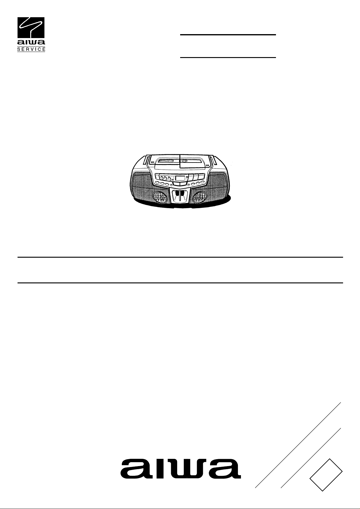
COMPACT DISC STEREO
RADIO CASSETTE RECORDER
This Service Manual is the "Revision Publishing" and replaces "Simple Manual"
BASIC TAPE MECHANISM : AZM-6 R1NF
BASIC CD MECHANISM : BZG-6 BNF
(S/M Code No. 09-014-355-7T1).
S/M Code No. 09-014-355-7R1
REVISION
DATA
SPECIFICATIONS
CSD-FD84 HRJ MODEL CSD-FD84 LH MODEL
Design and specifications are subject to change without
•
notice
.
Design and specifications are subject to change without
•
notice
.
CSD-FD82 U MODEL CSD-FD84 K, EZ MODEL
Design and specifications are subject to change without
•
notice
.
-2-
Design and specifications are subject to change without
•
notice
.
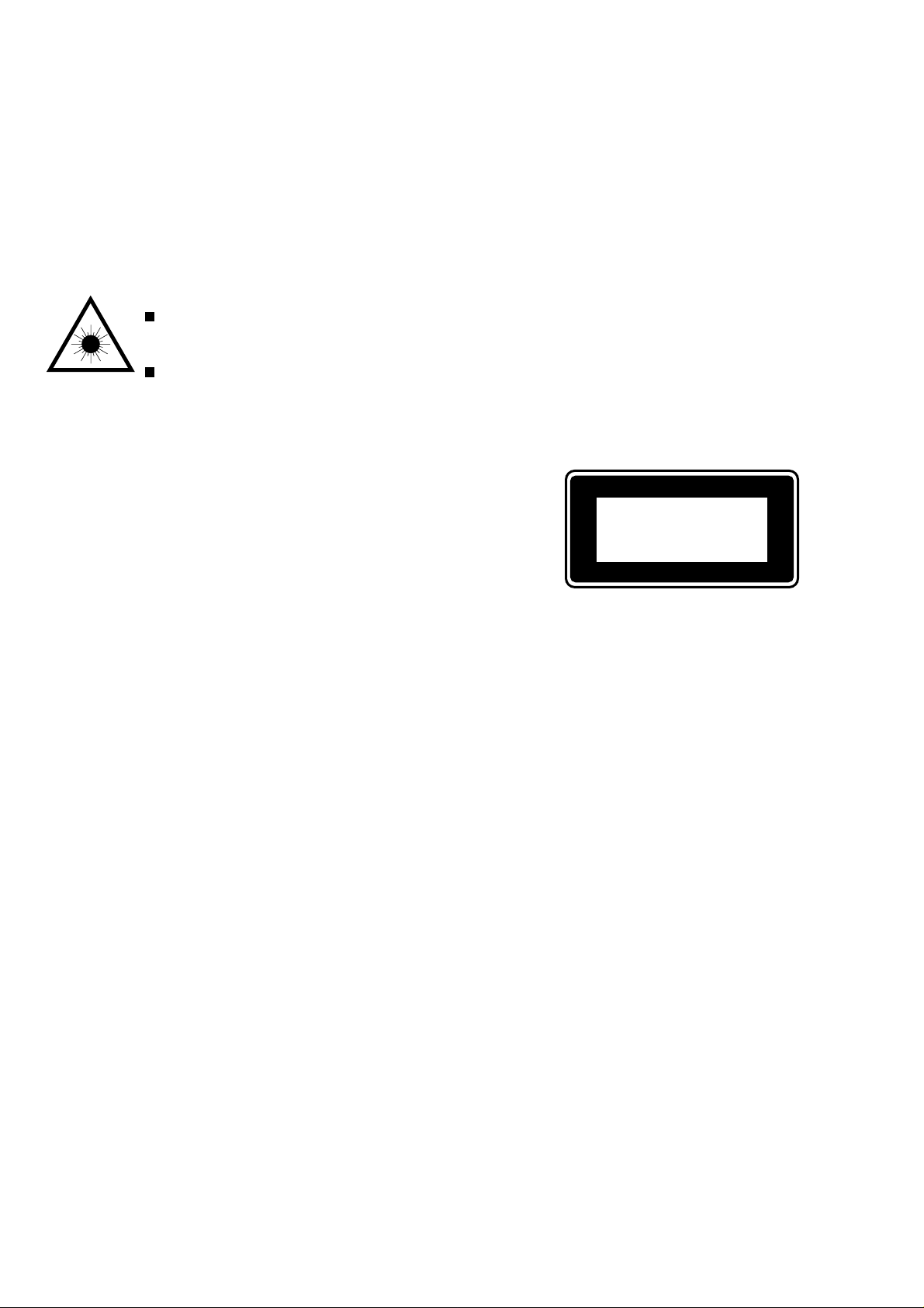
PROTECTION OF EYES FROM LASER BEAM DURING SERVICING
This set employs laser. Therefore, be sure to follow carefully the
instructions below when servicing.
WARNING!
WHEN SERVICING, DO NOT APPROACH THE LASER EXIT
WITH THE EYE TOO CLOSELY. IN CASE IT IS NECESSARY TO
CONFIRM LASER BEAM EMISSION. BE SURE TO OBSERVE
FROM A DISTANCE OF MORE THAN 30cm FROM THE
SURFACE OF THE OBJECTIVE LENS ON THE OPTICAL
PICK-UP BLOCK.
Caution: Invisible laser radiation when
open and interlocks defeated avoid exposure to beam.
Advarsel:Usynling laserståling ved åbning,
når sikkerhedsafbrydere er ude af funktion.
Undgå udsættelse for stråling.
VAROITUS!
Laiteen Käyttäminen muulla kuin tässä käyttöohjeessa mainitulla tavalla saattaa altistaa käyt-täjän turvallisuusluokan 1 ylittävälle näkymättömälle lasersäteilylle.
VARNING!
Om apparaten används på annat sätt än vad som specificeras i
denna bruksanvising, kan användaren utsättas för osynling
laserstrålning, som överskrider gränsen för laserklass 1.
CAUTION
Use of controls or adjustments or performance of procedures
other than those specified herein may result in hazardous
radiation exposure.
ATTENTION
L'utilisation de commandes, réglages ou procédures autres que
ceux spécifiés peut entraîner une dangereuse exposition aux
radiations.
ADVARSEL!
Usynlig laserståling ved åbning, når sikkerhedsafbrydereer ude
af funktion. Undgå udsættelse for stråling.
This Compact Disc player is classified as a CLASS 1 LASER
product.
The CLASS 1 LASER PRODUCT label is located on the rear
exterior.
CLASS 1
KLASSE 1
LUOKAN 1
KLASS 1
LASER PRODUCT
LASER PRODUKT
LASER LAITE
LASER APPARAT
-3-
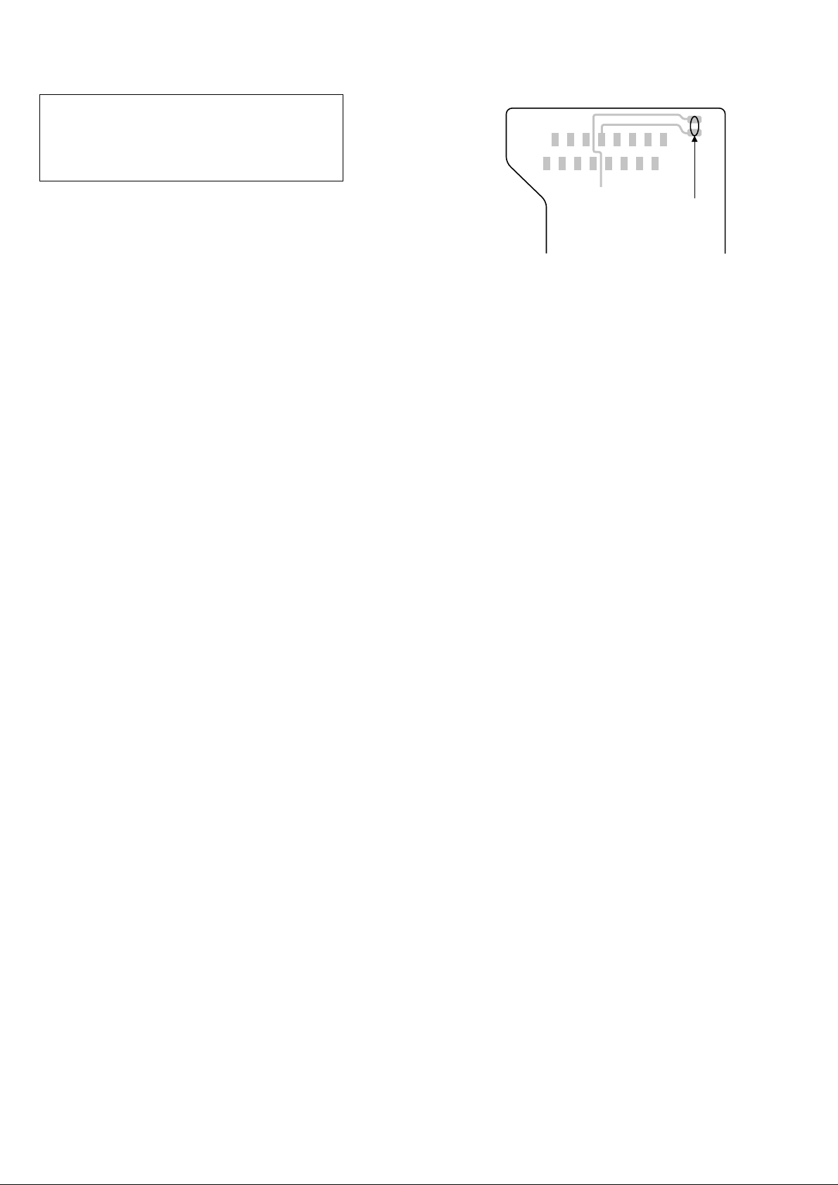
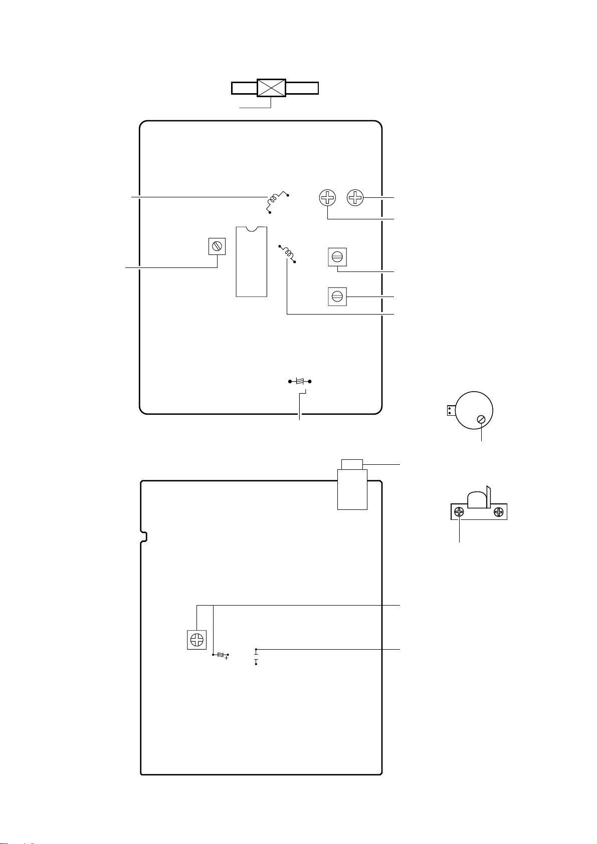
Precaution to replace Optical block
(PXR-104X-AP-0101)
Body or clothes electrostatic potential could ruin
laser diode in the optical block. Be sure ground
body and workbench, and use care the clothes
do not touch the diode.
1) After the connection, remove solder shown in
the right figure.
PICK-UP Assy PWB
Solder
-4-

ELECTRICAL MAIN PARTS LIST-1/4
REF. NO PART NO. KANRI DESCRIPTION
NO.
IC
87-A21-550-010 IC,TA2149N
87-A21-185-040 IC,LC72121D-N
87-020-454-010 IC,DN6851<FD84HRJSF,FD84LHSF>
8B-CH4-602-010 C-IC,LC867132V-BCH-4
87-A21-090-010 IC,LA4600
87-A21-520-040 C-IC,M61509FP
87-A20-911-010 IC,RPM6938
87-A21-419-040 C-IC,NJM14558MD-TE2
87-A20-446-010 C-IC,LA9241ML
87-A21-319-010 C-IC,LC78622NE
87-A21-891-010 C-IC,MM1469XH
TRANSISTOR
89-327-143-080 TR,2SC2714 (0.1W)
87-026-447-080 TR,2SC1740S R
89-111-624-080 TR,2SA1162Y
87-A30-288-040 C-TR,DTC114YKA
89-503-025-080 CHIP FET,2SK302 GR<FD84KSF,FD84EZSF>
89-320-011-080 TR,2SC2001 (15W)
87-A30-283-040 C-TR,DTA114YKA<FD84KSF,FD84EZSF>
89-327-125-080 CHIP TR,2SC2712GR
87-026-245-080 TR,DTC114ES<FD82USF>
87-A30-432-040 C-TR,DTC124XKA
87-026-463-080 TR,2SA933S (0.3W)
87-026-610-080 TR,KTC3198GR
87-A30-090-080 FET,2SK2541
89-110-155-080 TR,2SA1015(0.4W)
87-A30-190-080 TR,CC5551<FD84KSF,FD84EZSF>
86-NFZ-664-040 C-TR,DTC143TKA
87-A30-435-040 C-TR,DTC144EK T146
87-A30-287-040 C-TR,DTC114TKA
87-026-462-080 TR,2SC1740 S(RS 0.3W)
87-A30-433-040 C-TR,DTC143XKA
87-A30-427-040 C-TR,DTC114EKA
89-112-965-080 TR,2SA1296GR (0.75W)
87-A30-515-080 TR,2SA1979O/Y
87-A30-273-040 C-TR,DTC124EKA
89-109-521-080 TR,2SA952K (0.6W)
87-026-291-080 TR,DTC124XS
87-A30-492-080 TR,2SC5343G<FD84HRJSF>
87-A30-630-080 TR,2SC5343GL
89-213-702-010 TR,2SB1370 (1.8W)
DIODE
87-070-345-080 DIODE,IN4148
87-A40-616-070 VARI-CAP,SVC384(S/T)
87-A40-916-040 C-VARI-CAP,HVC202A
87-017-090-080 ZENER,HZS5B3
87-A40-530-080 DIODE,RB721Q-40
87-017-148-080 ZENER,HZS6A1L
87-A40-270-080 C-DIODE,MC2838
87-020-339-080 CHIP DIODE,1SS226
87-001-936-080 ZENER,HZS7A3L
87-001-731-080 ZENER,HZS6C2L
87-017-161-080 ZENER,HZS7C2L
87-020-465-080 DIODE,1SS133 (110MA)
87-A40-465-090 DIODE,FR202
MAIN C.B
C211 87-010-546-080 CAP, ELECT 0.33-50V
C212 87-010-546-080 CAP, ELECT 0.33-50V
C230 87-010-401-080 CAP, ELECT 1-50V
C233 87-010-546-080 CAP, ELECT 0.33-50V
C234 87-010-546-080 CAP, ELECT 0.33-50V
C235 87-A11-148-080 CAP,TC U 0.1-50 Z F
REF. NO PART NO. KANRI DESCRIPTION
NO.
C236 87-A11-148-080 CAP,TC U 0.1-50 Z F
C237 87-010-370-080 CAP,E 330-6.3 SME
C238 87-010-263-080 CAP, ELECT 100-10V
C239 87-012-286-080 CAP, U 0.01-25
C240 87-012-286-080 CAP, U 0.01-25
C241 87-010-400-080 CAP, ELECT 0.47-50V
C242 87-010-400-080 CAP, ELECT 0.47-50V
C243 87-010-401-080 CAP, ELECT 1-50V
C244 87-010-401-080 CAP, ELECT 1-50V
C245 87-010-401-080 CAP, ELECT 1-50V
C246 87-010-401-080 CAP, ELECT 1-50V
C247 87-010-402-080 CAP, ELECT 2.2-50V
C248 87-010-402-080 CAP, ELECT 2.2-50V
C255 87-A12-090-080 CAP,E 4.7-50 SMG
C263 87-012-274-080 CHIP CAP,U 1000P-50B
C264 87-012-274-080 CHIP CAP,U 1000P-50B
C265 87-010-544-080 CAP, ELECT 0.1-50V
C266 87-010-544-080 CAP, ELECT 0.1-50V
C271 87-A10-730-080 CAP,E 1000-16 SMG<EXCEPT FD82USF>
C271 87-A12-068-080 CAP,E 470-16 SMG<FD82USF>
C272 87-A10-730-080 CAP,E 1000-16 SMG<EXCEPT FD82USF>
C272 87-A12-068-080 CAP,E 470-16 SMG<FD82USF>
C273 87-012-274-080 CHIP CAP,U 1000P-50B
C274 87-018-131-080 CAP, CER 1000P-50V
C275 87-012-274-080 CHIP CAP,U 1000P-50B
C277 87-010-404-080 CAP, ELECT 4.7-50V
C278 87-A12-062-080 CAP,E 100-10 SMG
C279 87-A12-062-080 CAP,E 100-10 SMG
C287 87-012-273-080 C-CAP,U 820P-50 B
C288 87-012-273-080 C-CAP,U 820P-50 B
C289 87-012-156-080 C-CAP,S 220P-50 CH
C290 87-012-156-080 C-CAP,S 220P-50 CH
C301 87-012-275-080 C-CAP,U 1200P-50 B
C302 87-012-275-080 C-CAP,U 1200P-50 B
C305 87-A12-062-080 CAP,E 100-10 SMG
C306 87-A12-062-080 CAP,E 100-10 SMG
C307 87-012-285-080 C-CAP,U 8200P-50 B
C308 87-012-285-080 C-CAP,U 8200P-50 B
C311 87-010-546-080 CAP, ELECT 0.33-50V
C312 87-010-546-080 CAP, ELECT 0.33-50V
C313 87-012-283-080 C-CAP,U 5600P-50 B
C314 87-012-283-080 C-CAP,U 5600P-50 B
C321 87-018-205-080 CAP, CERA-SOL 0.022
C323 87-012-271-080 CAP, U 560P-50
C324 87-012-271-080 CAP, U 560P-50
C331 87-018-126-080 CAP,TC-U 390P-50 B
C332 87-018-126-080 CAP,TC-U 390P-50 B
C333 87-012-275-080 C-CAP,U 1200P-50 B
C334 87-012-278-080 C-CAP,U 2200P-50 B
C336 87-018-134-080 CAPACITOR,TC-U 0.01-16
C337 87-012-279-080 C-CAP,U 2700P-50 B
C338 87-012-279-080 C-CAP,U 2700P-50 B
C339 87-012-279-080 C-CAP,U 2700P-50 B
C340 87-A12-691-040 CAP,E 22-16 M 5L R85S5
C341 87-010-787-080 CAP, U 0.022-25
C342 87-012-266-080 C-CAP,U 220P-50 B<FD84KSF,FD84EZSF>
C343 87-012-284-080 CAP, U 6800P-50<FD84KSF,FD84EZSF>
C345 87-012-274-080 CHIP CAP,U 1000P-50B
C346 87-012-274-080 CHIP CAP,U 1000P-50B
C347 87-010-374-080 CAP, ELECT 47-10V
C348 87-012-274-080 CHIP CAP,U 1000P-50B
C350 87-012-275-080 C-CAP,U 1200P-50 B
C351 87-012-278-080 C-CAP,U 2200P-50 B
C352 87-012-284-080 CAP, U 6800P-50<FD84KSF,FD84EZSF>
C355 87-012-285-080 C-CAP,U 8200P-50 B
C356 87-012-285-080 C-CAP,U 8200P-50 B
C357 87-010-784-080 C-CAP,U 0.012-25 B
C358 87-010-784-080 C-CAP,U 0.012-25 B
C363 87-010-405-080 CAP, ELECT 10-50V
C364 87-010-405-080 CAP, ELECT 10-50V
-5-

ELECTRICAL MAIN PARTS LIST-2/4
REF. NO PART NO. KANRI DESCRIPTION
NO.
C367 87-012-273-080 C-CAP,U 820P-50 B
C368 87-012-273-080 C-CAP,U 820P-50 B
C369 87-012-193-080 C-CAP,U 82P-50 CH
C370 87-012-193-080 C-CAP,U 82P-50 CH
C373 87-010-401-080 CAP, ELECT 1-50V
C374 87-010-401-080 CAP, ELECT 1-50V
C382 87-010-401-080 CAP, ELECT 1-50V
C383 87-A12-063-080 CAP,E 220-10 SMG
C384 87-010-374-080 CAP, ELECT 47-10V
C387 87-012-266-080 C-CAP,U 220P-50 B<FD84KSF,FD84EZSF>
C401 87-010-403-080 CAP, ELECT 3.3-50V
C402 87-012-286-080 CAP, U 0.01-25
C403 87-A12-062-080 CAP,E 100-10 SMG
C404 87-A12-063-080 CAP,E 220-10 SMG
C405 87-012-286-080 CAP, U 0.01-25
C406 87-010-374-080 CAP, ELECT 47-10V
C407 87-012-274-080 CHIP CAP,U 1000P-50B
C408 87-010-787-080 CAP, U 0.022-25
C409 87-A12-063-080 CAP,E 220-10 SMG
C410 87-A12-062-080 CAP,E 100-10 SMG
C412 87-010-401-080 CAP, ELECT 1-50V
C413 87-A11-070-080 C-CAP,U 0.033-16 K B
C414 87-010-405-080 CAP, ELECT 10-50V
C416 87-010-545-080 CAP, ELECT 0.22-50V
C417 87-012-268-080 C-CAP,U 330P-50 B
C418 87-010-785-080 C-CAP,U0.015-25BK
C420 87-A11-070-080 C-CAP,U 0.033-16 K B
C422 87-012-279-080 C-CAP,U 2700P-50 B
C425 87-012-272-080 C-CAP,U 680P-50 B
C428 87-012-286-080 CAP, U 0.01-25
C429 87-012-282-080 CAP, U 4700P-50
C430 87-012-199-080 CAP 220P
C431 87-010-545-080 CAP, ELECT 0.22-50V
C432 87-010-374-080 CAP, ELECT 47-10V
C433 87-010-401-080 CAP, ELECT 1-50V
C434 87-012-280-080 CAP, U 3300P-50
C435 87-012-286-080 CAP, U 0.01-25
C436 87-010-374-080 CAP, ELECT 47-10V
C437 87-010-404-080 CAP, ELECT 4.7-50V
C439 87-012-274-080 CHIP CAP,U 1000P-50B
C440 87-012-162-080 C-CAP,U 1P-50 CK
C442 87-012-176-080 CAP 15P
C445 87-010-831-080 C-CAP,U,0.1-16F
C446 87-010-831-080 C-CAP,U,0.1-16F
C447 87-010-831-080 C-CAP,U,0.1-16F
C448 87-012-182-080 C-CAP,U 27P-50 CH
C451 87-012-199-080 CAP 220P
C455 87-A12-095-080 CAP,E 100-50 SMG
C457 87-012-176-080 CAP 15P
C458 87-012-176-080 CAP 15P
C459 87-A12-062-080 CAP,E 100-10 SMG
C460 87-010-197-080 CAP, CHIP 0.01 DM
C461 87-A11-132-080 CAP,TC U 0.01-50 K B
C462 87-A12-063-080 CAP,E 220-10 SMG
C463 87-A11-132-080 CAP,TC U 0.01-50 K B
C465 87-010-404-080 CAP, ELECT 4.7-50V
C466 87-010-831-080 C-CAP,U,0.1-16F
C467 87-A12-062-080 CAP,E 100-10 SMG
C469 87-A11-092-080 CAP,TC U 150P-50 J CH
C471 87-018-209-080 CAP, CER 0.1-50V
C472 87-018-209-080 CAP, CER 0.1-50V
C473 87-018-209-080 CAP, CER 0.1-50V
C474 87-018-209-080 CAP, CER 0.1-50V
C475 87-012-286-080 CAP, U 0.01-25
C476 87-A12-064-080 CAP,E 1000-10 SMG
C477 87-012-286-080 CAP, U 0.01-25
C478 87-A12-062-080 CAP,E 100-10 SMG
C479 87-012-286-080 CAP, U 0.01-25
C480 87-016-459-080 CAP,E 470-10 SMG
C481 87-010-405-080 CAP, ELECT 10-50V
REF. NO PART NO. KANRI DESCRIPTION
C482 87-010-405-080 CAP, ELECT 10-50V
C489 87-018-209-080 CAP, CER 0.1-50V
C490 87-018-209-080 CAP, CER 0.1-50V
C491 87-A11-132-080 CAP,TC U 0.01-50 K B
C492 87-A12-064-080 CAP,E 1000-10 SMG
C493 87-012-277-080 C-CAP, U 1800P-50 B
C493 87-012-286-080 CAP, U 0.01-25<FD82USF>
C494 87-A11-132-080 CAP,TC U 0.01-50 K B
C495 87-012-277-080 C-CAP, U 1800P-50 B
C495 87-012-286-080 CAP, U 0.01-25<FD82USF>
C496 87-A11-057-080 C-CAP,U 0.1-16 K B
C501 87-010-831-080 C-CAP,U,0.1-16F
C502 87-012-195-080 C-CAP,U 100P-50CH
C503 87-012-195-080 C-CAP,U 100P-50CH
C504 87-012-195-080 C-CAP,U 100P-50CH
C505 87-012-195-080 C-CAP,U 100P-50CH
C506 87-012-195-080 C-CAP,U 100P-50CH
C520 87-010-405-080 CAP, ELECT 10-50V
!
C521 87-A12-777-090 CAP,E 3300-25 M 85 SKR
C526 87-010-404-080 CAP, ELECT 4.7-50V
C527 87-010-401-080 CAP, ELECT 1-50V
C528 87-016-459-080 CAP,E 470-10 SMG
C529 87-A12-062-080 CAP,E 100-10 SMG
C530 87-A12-063-080 CAP,E 220-10 SMG
C531 87-010-265-080 CAP, ELECT 33-16V
C536 87-A12-062-080 CAP,E 100-10 SMG
CN203 87-049-469-010 CONN,4P V
CN205 87-A60-619-010 CONN,2P V 2MM JMT
CN302 87-099-832-010 CONN,8P S2M-8W
CN401 87-A60-424-010 CONN,16P V TOC-B
CN501 87-049-919-010 CONN,3P EH V WHT
CN801 87-A60-054-010 CONN,14P V 9604S-14C
CN802 87-A60-054-010 CONN,14P V 9604S-14C
CNA220 88-805-062-010 CONN ASSY,6P 200MM
CNA402 88-805-060-830 CONN ASSY,6P 80MM
J201 87-A60-420-010 JACK,3.5 ST (MSC)
!
J701 87-A61-455-010 JACK,AC E PSE27<EXCEPT FD82USF>
!
J701 87-A60-177-010 JACK,AC U W/SW<FD82USF>
JW437 87-003-098-080 COIL,2.2UH<EXCEPT FD84LHSF>
JW447 87-003-098-080 COIL,2.2UH<EXCEPT FD84LHSF>
L201 87-003-097-080 COIL,1UH
L202 87-003-097-080 COIL,1UH
L331 87-007-342-010 COIL,OSC 85K BIAS
L401 87-005-152-080 COIL,10UH
L402 87-003-146-080 COIL,15UH LAL02<EXCEPT FD84LHSF>
L404 87-005-239-080 COIL,100UH
L405 87-003-098-080 COIL,2.2UH<EXCEPT FD84LHSF>
R561 87-029-125-010 FUSE RESISTOR,1/4-1<FD82USF>
!
S501 87-A91-369-010 SW,AC SL 2 2 2 SDKGA41700<FD84LHSF>
SFR430 87-024-437-080 SFR100K,RH063EC
X401 81-592-641-010 VIB,CER 16.93MHZ
FRONT C.B
C120 87-010-178-080 CHIP CAP 1000P
C201 87-012-286-080 CAP, U 0.01-25
C202 87-A12-686-040 CAP,E 2.2-50 M 5L R85S5
C203 87-A12-686-040 CAP,E 2.2-50 M 5L R85S5
C204 87-A12-683-040 CAP,E 0.47-50 M 5L R85S5
C205 87-010-831-080 C-CAP,U,0.1-16F
C206 87-010-178-080 CHIP CAP 1000P
C221 87-A10-189-040 CAP,E 220-10
C222 87-010-196-080 CHIP CAPACITOR,0.1-25
C223 87-010-550-040 CAP,E 100-6.3 GAS
C225 87-010-805-080 CAP, S 1-16
C226 87-010-178-080 CHIP CAP 1000P
C227 87-012-286-080 CAP, U 0.01-25
C228 87-012-178-080 C-CAP,U 18P-50 CH
<EXCEPT FD84LHSF,FD82USF>
<EXCEPT FD84LHSF,FD82USF>
NO.
-6-

ELECTRICAL MAIN PARTS LIST-3/4
REF. NO PART NO. KANRI DESCRIPTION
C229 87-012-180-080 C-CAP,U 22P-50 CH
C230 87-012-186-080 C-CAP,U 39P-50 CH
C231 87-012-186-080 C-CAP,U 39P-50 CH
C232 87-012-176-080 CAP 15P
C233 87-A10-047-080 C-CAP,U 1-10 Z F
C241 87-A12-689-040 CAP,E 10-16 M 5L R85S5
C242 87-012-274-080 CHIP CAP,U 1000P-50B
C261 87-012-286-080 CAP, U 0.01-25
C331 87-012-286-080 CAP, U 0.01-25
C332 87-012-286-080 CAP, U 0.01-25
C333 87-A12-689-040 CAP,E 10-16 M 5L R85S5
C334 87-A12-689-040 CAP,E 10-16 M 5L R85S5
C335 87-010-831-080 C-CAP,U,0.1-16F
C336 87-010-831-080 C-CAP,U,0.1-16F
C337 87-010-549-040 CAP,E 47-6.3 GAS
C338 87-010-549-040 CAP,E 47-6.3 GAS
C351 87-010-555-040 CAP,E 100-10 GAS
C352 87-012-286-080 CAP, U 0.01-25
C401 87-010-831-080 C-CAP,U,0.1-16F
C403 87-010-982-040 CAP,E 33-25 GAS
C511 87-010-263-040 CAP,E 100-10
C512 87-A12-063-040 CAP,E 220-10 SMG
C515 87-012-286-080 CAP, U 0.01-25
CN501 87-099-755-010 CONN,14P H 9604
CN502 87-099-755-010 CONN,14P H 9604
CN503 87-A60-080-010 CONN,07P H 9604S-07F
CNA501 88-803-042-260 CONN ASSY,4P 220MM
D333 87-A92-157-010 LED,SMLU1BE16C-S
D351 8A-CDA-646-010 LED,6224-10GD GRN
JW216 87-003-098-080 COIL,2.2UH<FD82USF>
L222 87-003-097-080 COIL,1UH
LCD301 8B-CH4-605-010 LCD,AIW4267BCH-4
S301 87-A91-704-080 SW,TACT EVQ 214 05R
S302 87-A91-704-080 SW,TACT EVQ 214 05R
S303 87-A91-704-080 SW,TACT EVQ 214 05R
S304 87-A91-704-080 SW,TACT EVQ 214 05R
S305 87-A91-704-080 SW,TACT EVQ 214 05R
S306 87-A91-704-080 SW,TACT EVQ 214 05R
S307 87-A91-704-080 SW,TACT EVQ 214 05R
S308 87-A91-704-080 SW,TACT EVQ 214 05R
S311 87-A91-704-080 SW,TACT EVQ 214 05R
S312 87-A91-704-080 SW,TACT EVQ 214 05R
S313 87-A91-704-080 SW,TACT EVQ 214 05R
S314 87-A91-704-080 SW,TACT EVQ 214 05R
S315 87-A91-704-080 SW,TACT EVQ 214 05R
S316 87-A91-704-080 SW,TACT EVQ 214 05R
S317 87-A91-704-080 SW,TACT EVQ 214 05R
S318 87-A91-704-080 SW,TACT EVQ 214 05R
S319 87-A91-704-080 SW,TACT EVQ 214 05R
X201 87-030-273-010 VIB,XTAL 32.768K5PPM
X202 87-A70-070-080 VIB,CER 5.76MHZ CRHF
POWER C.B
C701 87-018-205-080 CAP, CERA-SOL 0.022
C702 87-018-205-080 CAP, CERA-SOL 0.022
C703 87-018-205-080 CAP, CERA-SOL 0.022
C704 87-018-205-080 CAP, CERA-SOL 0.022
CNA701 8B-CH4-662-110 CONN ASSY,3P V PWR
!
F701 87-A91-216-010 FUSE,2.5A 250V T 50TEXCEPT FD82USF>
FC701 87-033-213-080 CLAMP, FUSE<EXCEPT FD82USF>
FC702 87-033-213-080 CLAMP, FUSE<EXCEPT FD82USF>
TUNER C.B
C1 87-010-312-080 C-CAP,S 15P-50 CH
C2 87-010-316-080 C-CAP,S 33P-50 CH
C3 87-010-312-080 C-CAP,S 15P-50 CH
C5 87-016-669-080 C-CAP,S 0.1-25 K B
NO.
<EXCEPT FD84KSF,FD84EZSF>
REF. NO PART NO. KANRI DESCRIPTION
NO.
C5 87-012-360-080 CAP, CER 1-10<FD84KSF,FD84EZSF>
C6 87-010-313-080 CAP, CHIP 18P<EXCEPT FD84KSF,FD84EZSF>
C7 87-012-140-080 CAP 470P
C8 87-012-349-080 C-CAP,S 1000P-50 CH
C10 87-010-197-080 CAP, CHIP 0.01 DM
C11 87-010-197-080 CAP, CHIP 0.01 DM
C12 87-010-197-080 CAP, CHIP 0.01 DM
C13 87-010-150-080 C-CAP,S 6P-50 CH
C14 87-012-157-080 C-CAP,S 330P-50 CH
C15 87-010-178-080 CHIP CAP 1000P
C16 87-010-374-080 CAP, ELECT 47-10V
C17 87-010-198-080 CAP, CHIP 0.022
C18 87-010-992-080 C-CAP,S 0.047-25 B
C19 87-A12-062-080 CAP,E 100-10 SMG
C20 87-010-404-080 CAP, ELECT 4.7-50V
C21 87-010-197-080 CAP, CHIP 0.01 DM
C22 87-010-197-080 CAP, CHIP 0.01 DM
C23 87-010-197-080 CAP, CHIP 0.01 DM
C24 87-012-157-080 C-CAP,S 330P-50 CH
C25 87-016-460-080 C-CAP,S 0.22-16 B
C27 87-A11-067-080 C-CAP,S 1-10 K B
C28 87-016-669-080 C-CAP,S 0.1-25 K B
C29 87-016-669-080 C-CAP,S 0.1-25 K B
C30 87-010-220-080 C-CAP,S 0.018-25 B
<EXCEPT FD84LHSF,FD82USF>
C30 87-012-365-080 C-CAP,S 0.027-25VBK<FD84LHSF,FD82USF>
C31 87-010-220-080 C-CAP,S 0.018-25 B
<EXCEPT FD84LHSF,FD82USF>
C31 87-012-365-080 C-CAP,S 0.027-25VBK<FD84LHSF,FD82USF>
C33 87-012-358-080 C-CAP,S 0.47-10 F Z
C34 87-012-358-080 C-CAP,S 0.47-10 F Z
C35 87-010-197-080 CAP, CHIP 0.01 DM
C36 87-A12-062-080 CAP,E 100-10 SMG
C37 87-010-197-080 CAP, CHIP 0.01 DM
C38 87-A12-062-080 CAP,E 100-10 SMG
C39 87-010-404-080 CAP, ELECT 4.7-50V
C40 87-010-197-080 CAP, CHIP 0.01 DM
C41 87-010-178-080 CHIP CAP 1000P
C42 87-010-178-080 CHIP CAP 1000P
C43 87-010-178-080 CHIP CAP 1000P
C44 87-010-312-080 C-CAP,S 15P-50 CH<FD82USF>
C44 87-010-311-080 CAP 12P<EXCEPT FD82USF>
C45 87-010-312-080 C-CAP,S 15P-50 CH
C46 87-010-197-080 CAP, CHIP 0.01 DM
C47 87-010-197-080 CAP, CHIP 0.01 DM
C48 87-010-197-080 CAP, CHIP 0.01 DM
C49 87-012-140-080 CAP 470P
C50 87-010-197-080 CAP, CHIP 0.01 DM
C51 87-010-316-080 C-CAP,S 33P-50 CH<FD84KSF,FD84EZSF>
C52 87-010-197-080 CAP, CHIP 0.01 DM<FD84KSF,FD84EZSF>
C53 87-010-197-080 CAP, CHIP 0.01 DM<FD84KSF,FD84EZSF>
C54 87-010-177-080 C-CAP,S 820P-50 SL<FD84KSF,FD84EZSF>
C55 87-010-197-080 CAP, CHIP 0.01 DM<FD84KSF,FD84EZSF>
C56 87-010-312-080 C-CAP,S 15P-50 CHFD84KSF,FD84EZSF>
C71 87-010-197-080 CAP, CHIP 0.01 DM
C72 87-A12-062-080 CAP,E 100-10 SMG
C73 87-010-197-080 CAP, CHIP 0.01 DM
C75 87-010-197-080 CAP, CHIP 0.01 DM
C92 87-010-197-080 CAP, CHIP 0.01 DM
C93 87-010-197-080 CAP, CHIP 0.01 DM
CF2 87-008-261-010 FILTER, SFE10.7MA5-A
CF3 87-008-261-010 FILTER, SFE10.7MA5-A
CN2 87-A60-623-010 CONN,6P V 2MM JMT
CN3 87-A60-621-010 CONN,4P V 2MM JMT
L2 87-A50-560-010 COIL,FM BPF(ACD)
L4 87-A50-420-010 COIL,MW OSC(SYN)
L5 87-A50-566-010 COIL,FM RF EX(ACH)
L6 87-A50-567-010 COIL,FM OSC(ACH)
L7 87-A91-308-010 FLTR,PCFAZH- 450T (TOK)
L8 87-005-849-080 COIL,10UH(CECS)
-7-
ELECTRICAL MAIN PARTS LIST-4/4
REF. NO PART NO. KANRI DESCRIPTION
NO.
L51 87-A50-421-010 COIL,LW OSC(SYN)<FD84KSF,FD84EZSF>
L003 8A-CH4-670-010 BAR-ANT,MW 2B-ACH(COI)
<EXCEPT FD84KSF,FD84EZSF>
L003 8A-CH4-671-010 BAR-ANT,MW/LW 3B-ACH(COI)
<FD84KSF,FD84EZSF>
TC1 87-011-254-080 TRIMER,20P LAR
TC51 87-A92-234-080 TRIMMER,50P 4-4.5 LAR<FD84KSF,FD84EZSF>
X1 87-A70-061-010 VIB,XTAL 4.500MHZ CSA-309
SPL C.B
C293 87-010-133-080 CAP, ELECT 2.2-50V
CN291 87-A60-619-010 CONN,2P V 2MM JMT
CNA203 8B-CH4-655-010 CONN ASSY,4P V SP
SPR C.B
C294 87-010-133-080 CAP, ELECT 2.2-50V
CN292 87-A60-619-010 CONN,2P V 2MM JMT
REF. NO PART NO. KANRI DESCRIPTION
NO.
DECK C.B
CN1 87-A60-080-010 CONN,07P H 9604S-07F
SW1 87-A90-673-010 SW,MICRO ESE11SH1C
SW2 87-A90-673-010 SW,MICRO ESE11SH1C
SW3 87-A90-673-010 SW,MICRO ESE11SH1C
MOTOR C.B
CN1 87-A60-670-010 CONN,6P H 2MM JMT
M1 87-A91-973-010 MOT,MDN4RA3FTAS1
M2 87-045-363-010 MOT,MDN4RA3ETA1
SW1 87-A90-042-010 SW,LEAF MSW-17310MVP0
• Regarding connectors, they are not stocked as they are not the initial order items.
The connectors are available after they are supplied from connector manufacturers upon the order is received.
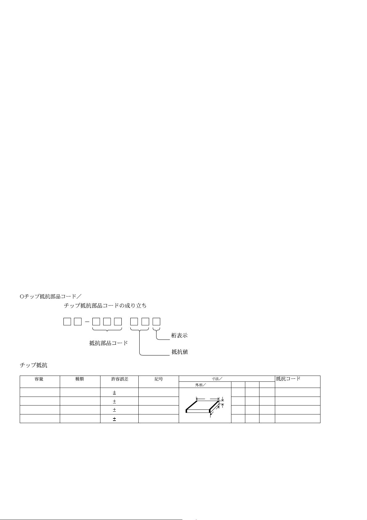
CHIP RESISTOR PART CODE
Chip Resistor Part Coding
88
A
Resistor Code
Chip resistor
Wattage Type Tolerance
1/16W 1005 5% CJ
1/16W
1/10W
1/8W
1608
2125
3216
5%
5%
5%
Symbol
Figure
Value of resistor
CJ
CJ
CJ
Form
L
W
Dimensions (mm)
LW t
1.0 0.5 0.35 104
t
1.6 0.8 0.45
2 1.25 0.45
1.6
0.55
3.2
Resistor Code
108
118
128
: A
: A
-8-
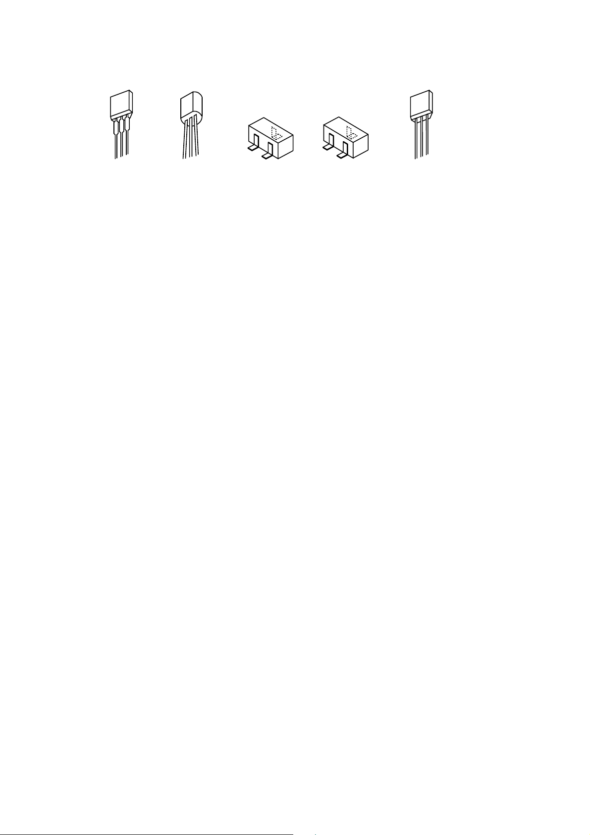
TRANSISTOR ILLUSTRATION-1/1
ECB
2SA933
ECB
2SA952
2SA1296
2SC1740
2SC2001
CC5551
KTC3198
2SA1015
2SC5343
2SA19790
C
B
E
2SA1162
2SC2714
DTA114YK
DTC114YK
DTC124XK
DTC144EK
S
D
G
2SK302GR
ECB
2SK2541
-9-
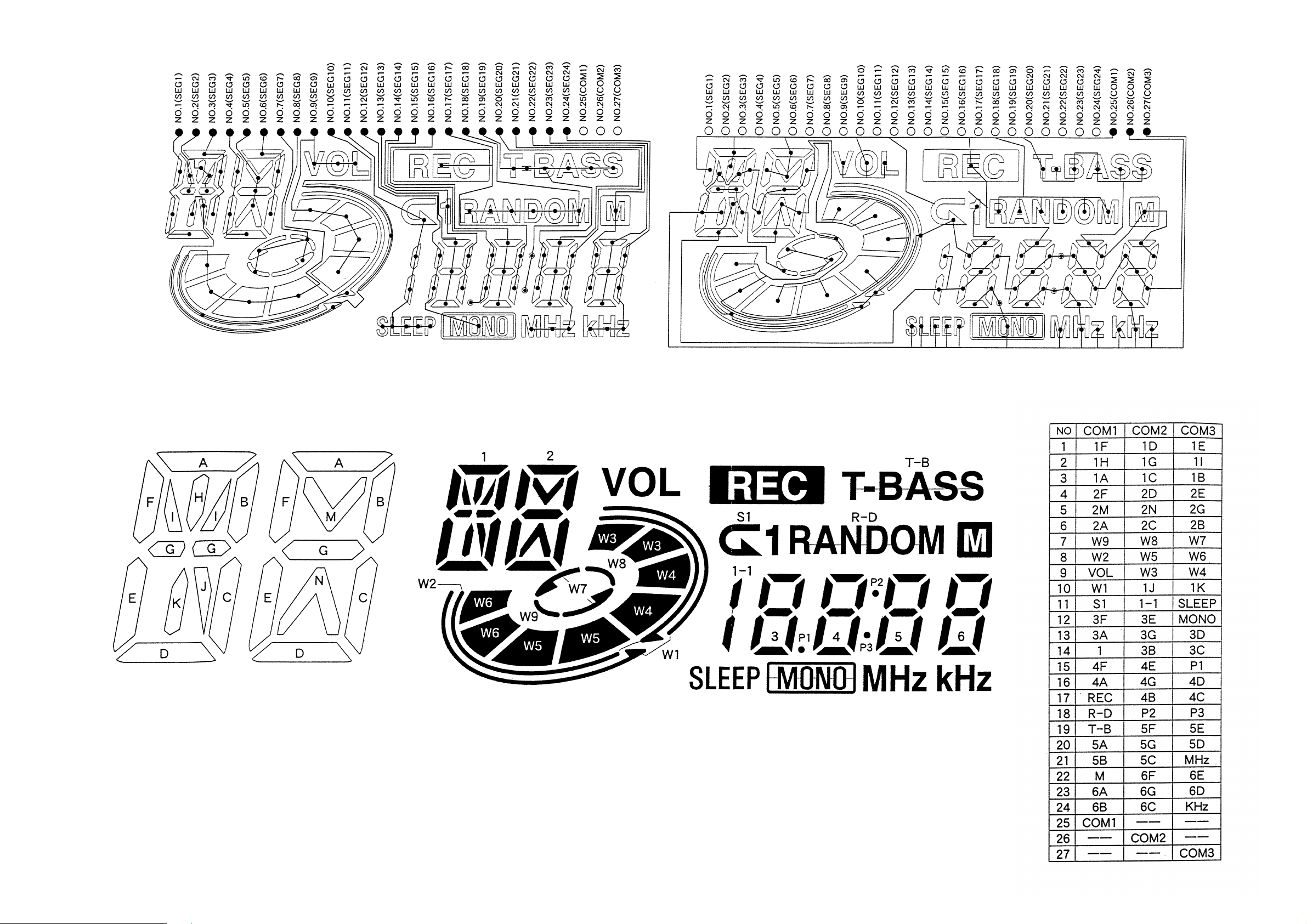
FL (LCD, AIW4267BCH-4) GRID ASSIGNMENT/ANODE CONNECTION-1/1
GRID ASSIGNMENT
ANODE CONNECTION
-10-
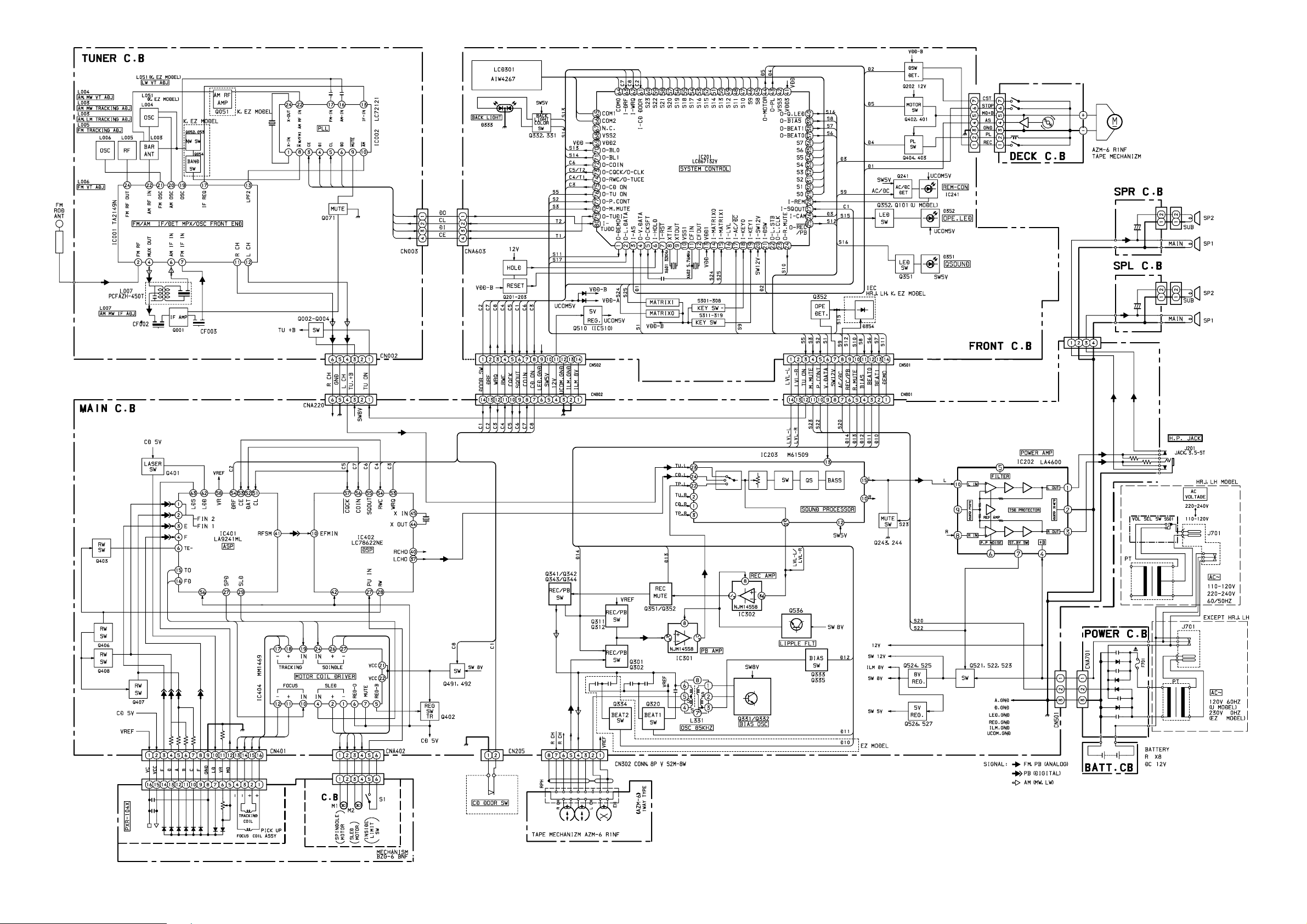
BLOCK DIAGRAM-1/1
CN1
CN503
CN292
CN291
CNA203
CN203
MOTOR
-11-
5
, K
14
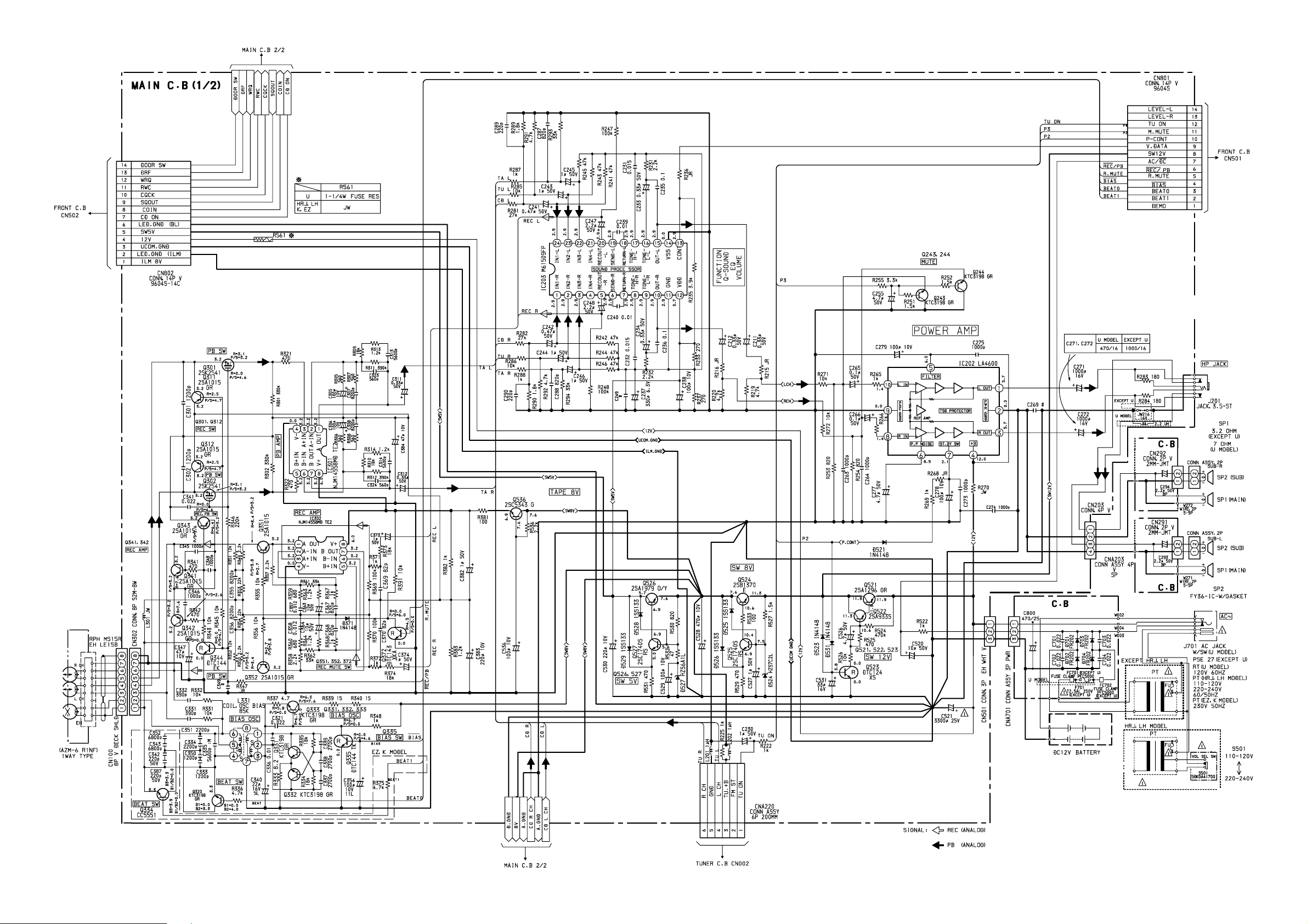
SCHEMATIC DIAGRAM-1/5 (MAIN)
POWER
SPR
SPL
BATT C.B
-12-
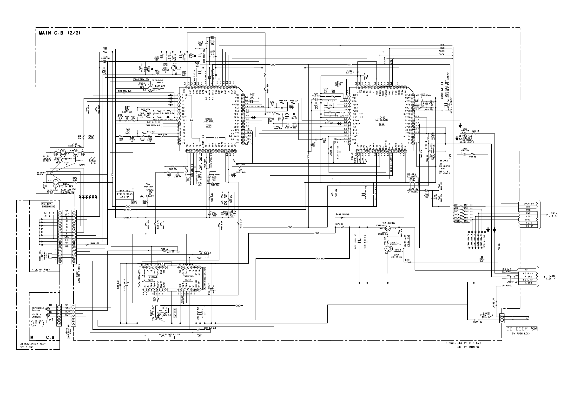
SCHEMATIC DIAGRAM-2/5 (CD)
OTOR
2
2
-13-

WIRING-1/6 (MAIN, CD)
101112131415161718192021222324
1234567892526272829303132
A
B
C
D
E
F
G
H
BNF
PICK UP
BNF
MOTOR C.B CN1
R1NF
I
J
K
L
M
N
O
P
Q
R
-14-
S
T
U

WIRING-2/6 (POWER, BATT, VOL SEL)
123456789101112131415
A
B
C
D
E
MAIN C.B
CN501
800
F
G
H
BATTERY DC
12V R14 8
I
J
K
L
M
N
-15-
O
P
Q
R
S
T
U

SCHEMATIC DIAGRAM-3/5 (FRONT)
-16-
NO MOUNT
NO MOUNT
NO MOUNT
NO MOUNT

WIRING-3/6 (FRONT)
FRONT C.B
101112131415161718192021222324
1234567892526272829303132
A
B
C
D
E
F
G
H
I
J
K
L
M
N
O
P
Q
-17-
R
S
T
U

SCHEMATIC DIAGRAM-4/5 (TUNER HRJ, LH, U)
L003, TC001 L004 L005 L006
AM TRACKING ADJ FM TRACKING ADJAM VT ADJ FM VT ADJ
-18-
FRONT
CNA501
~
1/2
CNA220

WIRING-4/6 (TUNER HRJ, LH, U)
123456789101112131415
A
B
C
D
E
F
G
H
I
J
K
L
M
N
O
P
Q
-19-
R
S
T
U

SCHEMATIC DIAGRAM-5/5 (TUNER K, EZ)
-20-
1/2

WIRING-5/6 (TUNER K,EZ)
123456789101112131415
A
B
C
D
E
F
G
H
I
J
K
L
M
N
O
P
Q
-21-
R
S
T
U

WIRING-6/6 (DECK, MOTOR)
123456789101112131415
A
(AZM6 R1NF)
FRONT C.B CN503
MOTOR C.B (BZG6 BNF)
B
C
D
E
F
G
H
I
J
CN1
M1
K
M1
SPINDLE
L
MOTOR
M
SW1
N
SW1
(LIMIT SW)
O
P
M2
Q
R
M2
SLED
S
MOTOR
16
T
MAIN C.B
CNA402
U
-22-

ELECTRICAL ADJUSTMENT-1/4 (HRJ, LH, U)
L003
(BAR-ANT)
TUNER C.B
5
13
3
L007
IC001
L005
L006
+
TC001
3
L004
2
4
DECK
C39
MAIN C.B
SFR430
C433
C441
24
M1
(DECK MOTOR)
6
67
RPH
7
8
8
-23-

ELECTRICAL ADJUSTMENT-2/4 (HRJ, LH, U)
< TUNER SECTION >
1. AM IF Adjustment
L007 ............................................................ 1400/1404kHz
2. AM VT Adjustment
Settings: • Test point: C39+
• Adjustment location: L004
Method: Set to AM 1602/1710kHz adjust L004 so that the test
point becomes 6.0V±50mV (U, LH) set to AM 1602/
1710 kHz adjust L004 so that the Test point becomes
5.6V±50mV (HRJ).
3. AM Tracking Adjustment
L003 ....................................................................... 600kHz
TC001................................................................... 1400kHz
4. FM VT Adjustment
Settings: • Test point: C39+
• Adjustment location: L006
Method: Set to FM 108MHz adjust L006 so that the test point
becomes 6.0V±50mV.
5. FM Tracking Adjustment
L005 .....................................................................87.5MHz
< DECK SECTION >
6. Tape speed Adjustment
Settings: • Test tape: TTA-100
• Test point: PHONES JACK (J201)
• Adjustment location: SFR of deck motor
Method: Play back the test tape and adjust so that the output
frequency is 3000Hz ±30Hz.
7. Azimuth Adjustment
Settings: • Test tape: TTA-320
• Test point: PHONES JACK (J201)
• Adjustment location:Azimuth adjustment screw
Method: Play back the test tape and adjust so that the output is
maximum.
< CD SECTION >
8. Focus BIAS Adjustment
Settings: • Test CD: D-782
• Test point: C441 (RF OUT)
C433- (VREF)
• Adjustment location: SFR430
Method: Play back the test CD track 2 and adjust so that the
output level is DC 0mV±10mV.
-24-
ELECTRICAL ADJUSTMENT-3/4 (K, EZ)
L003
(BAR-ANT)
TUNER C.B
5
13
37
L007
IC001
L005
L006
C39
+
TC051
L004
L051
TC001
7
3
2
6
4
DECK
MAIN C.B
SFR430
C433
C441
246
M1
(DECK MOTOR)
8
89
RPH
J201
9
0
0
-25-

ELECTRICAL ADJUSTMENT-4/4 (K, EZ)
< TUNER SECTION >
1. MW IF Adjustment
L007 ............................................................ 1400/1404kHz
2. MW VT Adjustment
Settings: • Test point: C39+
• Adjustment location: L004
Method: Set to MW 1602/1710kHz adjust L004 so that the test
point becomes 5.6V±50mV.
3. MW Tracking Adjustment
L003 ....................................................................... 603kHz
TC051................................................................... 1404kHz
4. FM VT Adjustment
Settings: • Test point: C39+
• Adjustment location: L006
Method: Set to FM 108MHz adjust L006 so that the test point
becomes 6.0V±50mV.
5. FM Tracking Adjustment
L005 .....................................................................87.5MHz
6. LW VT Adjustment
Settings: • Test point: C39+
• Adjustment location: L051
Method: Set to LW 290kHz adjust L051 so that the test point
becomes 4.60V±50mV.
< DECK SECTION >
8. Tape speed Adjustment
Settings: • Test tape: TTA-100
• Test point: PHONES JACK (J201)
• Adjustment location: SFR of deck motor
Method: Play back the test tape and adjust so that the output
frequency is 3000Hz ±30Hz.
9. Azimuth Adjustment
Settings: • Test tape: TTA-320
• Test point: PHONES JACK (J201)
• Adjustment location:Azimuth adjustment screw
Method: Play back the test tape and adjust so that the output is
maximum.
< CD SECTION >
10. Focus BIAS Adjustment
Settings: • Test CD: TCD-782
• Test point: C441 (RF OUT)
C433- (VREF)
• Adjustment location: SFR430
Method: Play back the test CD track 2 and adjust so that the
output level is DC 0mV±10mV.
7. LW Tracking Adjustment
L003 ....................................................................... 153kHz
TC001..................................................................... 288kHz
-26-

IC DESCRIPTION-1/3 (LA9241ML)-1/2
Pin No. Pin Name I/O Description
1
FIN2
Pin to which external pickup photo diode is connected. RF signal is created by adding with the
I
FIN1 pin signal. FE signal is created by subtracting from the FIN1 pin signal.
10
11
12
13
14
15
16
2
3
4
5
6
7
8
9
FIN1
E
F
TB
TE-
TE
TESI
SCI
TH
TA
TD-
TD
JP
TO
FD
I
Pin to which external pickup photo diode is connected.
Pin to which external pickup photo diode is connected. TE signal is created by subtracting from
I
the F pin signal.
I
Pin to which external pickup photo diode is connected.
I
DC component of the TE signal is input.
I
Pin to which external resistor setting the TE signal gain is connected between the TE pin.
O
TE signal output pin.
TES “Track Error Sense” comparator input pin. TE signal is passed through a band-pass filter
I
then input.
I
Shock detection signal input pin.
I
Tracking gain time constant setting pin.
O
TA amplifier output pin.
Pin to which external tracking phase compensation constants are connected between the TD and
I
VR pins.
I
Tracking phase compensation setting pin.
I
Tracking jump signal (kick pulse) amplitude setting pin.
O
Tracking control signal output pin.
O
Focusing control signal output pin.
17
18
19
20
21
22
23
24
25
26
27
28
29
30, 31
FD-
FA
FA-
FE
FE-
AGND
SP
SPI
SPG
SP-
SPD
SLEQ
SLD
SL-, SL+
Pin to which external focusing phase compensation constants are connected between the FD and
I
FA pins.
Pin to which external focusing phase compensation constants are connected between the FD–
I
and FA– pins.
Pin to which external focusing phase compensation constants are connected between the FA and
I
FE pins.
O
FE signal output pin.
I
Pin to which external FE signal gain setting resistor is connected between the FE pin.
—
Analog signal GND.
O
Signal ended output of the CV+and CV- pin input signal.
I
Spndle amp input.
I
Pin to which external spindle gain setting resistor in 12 cm mode is connected.
Pin to which external spindle phase compensation constants are connected together with SPD
I
pin.
O
Spindle control signal output pin.
I
Pin to which external sled phase compensation constants are connected.
O
Sled control signal output pin.
I
Sled advance signal input pin from microprocessor.
32, 33
34
35
JP-, JP+
TGL
TOFF
I
Tracking jump signal input pin from DSP.
I
Tracking gain control signal input from DSP. Low gain when TGL = H.
I
Tracking off control signal input pin from DSP. Off when TOFF = H.
-27-

IC DESCRIPTION-1/3 (LA9241ML)-2/2
Pin No. Pin Name I/O Description
36
TES
O
Pin from which TES signal is output to DSP.
37
38
39, 40
41
42
43
44
45
46
47
48
49
50
51
52
53
HFL
SLOF
CV–, CV+
RFSM
RFS-
SLC
SLI
DGND
FSC
TBC
NC
DEF
CLK
CL
DAT
CE
O
O
O
—
O
—
O
“High Frequency Level” is used to judge whether the main beam position is on top of bit or on
top of mirror.
I
Sled servo off control input pin.
I
CLV error signal input pin from DSP.
RF output pin.
I
RF gain setting and EFM signal 3T compensation constant setting pin together with RFSM pin.
“Slice Level Control” is the output pin which controls the RF signal data slice level by DSP.
I
Input pin which control the data slice level by the DSP.
Digital system GND.
Output pin to which external focus search smoothing capacitor is connected.
I
“Tracking Balance Control” EF balance variable range setting pin.
No connection.
Disc defect detector output pin.
I
Reference clock input pin. 4.23 MHz of the DSP is input.
I
Microprocessor command clock input pin.
I
Microprocessor command data input pin.
I
Microprocessor command chip enable input pin.
54
55
56
57
58
59
60
61
62
63
64
DRF
FSS
VCC2
REFI
VR
LF2
PHI
BHI
LDD
LDS
VCC1
O
“Detect RF” RF level detector output.
I
“Focus Search Select” focus search mode (± search/+ search) select pin. (Not connected)
—
Servo system and digital system Vcc pin.
—
Pin to which external bypass capacitor for reference voltage is connected.
O
Reference voltage output pin.
I
Disc defect detector time constant setting pin.
I
Pin to which external capacitor for RF signal peak holding is connected.
I
Pin to which external capacitor for RF signal bottom holding is connected.
O
APC circuit output pin.
I
APC circuit input pin.
—
RF system Vcc pin.
-28-
IC DESCRIPTION-2/3 (LC78622NE)-1/2
Pin No. Pin Name I/O Description
1
DEFI
I
Defect sense signal (DEF) input pin. (Connect to 0V when not used)
2
3
4
5
6
7
8
9
10
11
12, 13
14
15
16
17
18
TAI
PDO
VVSS
ISET
VVDD
FR
VSS
EFMO
EFMIN
T2
CLV+, CLK-
__
V/P
HFL
TES
TOFF
TGL
I
O
—
For PLL.
I
—
I
—
Digital system GND. Be sure to connect to 0V.
O
For slice level control.
I
I
Test signal input pin with built-in pull-down resistor. Be sure to connect to 0V.
O
Disc motor control output. Three level output is possible using command.
Rough servo or phase control automatic selection monitoring output pin. Rough servo at H.
O
Phase servo at L.
I
Track detect signal input pin. Schmidt input.
I
Tracking error signal input pin. Schmidt input.
O
Tracking OFF output pin.
O
Tracking gain selection output pin. Gain boost at L.
Test signal input pin with built-in pull-down resistor. Be sure to connect to 0V.
Phase comparator output pin to control external VCO.
GND pin for built-in VCO. Be sure to connect to 0V.
Pin to which external resistor adjusting the PD0 output current.
Power supply pin for built-in VCO.
Pin for VCO frequency range adjustment.
EFM signal output pin.
EFM signal input pin.
19, 20
21
22
23
24
25
26
27
28
29
30
31
32, 33
34
35
36
37
JP+, JP-
PCK
FSEQ
VDD
SL+
SL-
COM3
PUIN
RW
EMPH
C2F
DOUT
T3, T4
N.C.
MUTEL
LVDD
LCHO
O
O
O
—
O
O
I/O
O
O
O
O
—
O
—
O
Track jump control signal output pin. Three level output is possible using command.
EFM data playback clock monitoring pin 4.3218 MHz when phase is locked in. (Not connected)
Sync signal detection output pin. H when the sync signal which is detected from EFM signal and
thesync signal which is internally generated agree. (Not connected)
Digital system power supply pin.
Moves the sled to outer circumference.
Moves the sled to inner circumference.
General purpose input/output pin.
I
CD pickup inner switch detection.
Read, wright signal.
De-emphasis monitor output pin. De-emphasis disc is being played back at H. (Not connected)
C2 flag output pin. (Not connected)
DIGITAL OUT output pin. (EIAJ format) (Not connected)
I
Test signal input pin with built-in pull-down resistor. Be sure to connect to 0V.
Not connected. Set the pin to open.
L-channel mute output pin. (Not connected)
L-channel 1-bit DAC.
L-channel power supply pin.
L-channel output pin.
38
39
40
41
42
LVSS
RVSS
RCHO
RVDD
MUTER
—
—
O
R-channel 1-bit DAC.
—
O
L-channel GND. Be sure to connect to 0V.
R-channel GND. Be sure to connect to 0V.
R-channel output pin.
R-channel power supply pin.
R-channel mute output pin. (Not connected)
-29-

IC DESCRIPTION-2/3 (LC78622NE)-2/2
Pin No. Pin Name I/O Description
43
XVDD
—
Crystal oscillator power supply pin.
44
45
46
47
48
49
50
51
52
53
54
55
56
57
58
XOUT
XIN
XVSS
SBSY
EFLG
PW
SFSY
SBCK
FSX
WRQ
RWC
SQOUT
COIN
____________
CQCK
RES
O
Pin to which external 16.9344 MHz crystal oscillator is connected.
I
—
Crystal oscillator GND pin. Be sure to connect to 0V.
O
Subcode block sync signal output pin. (Not connected)
O
C1, C2, single and dual correction monitoring pin. (Not connected)
O
Subcode P, Q, R, S, T, U and W output pin. (Not connected)
Subcode frame sync signal output pin. Falls down when subcode enters standby.
O
(Not connected)
I
Subcode read clock input pin. Schmidt input. (Be sure to connected to 0V when not in use)
Pin outputting the 7.35 kHz sync signal which is generated by dividing frequency of crystal
O
oscillator. (Not connected)
O
Subcode Q output standby output pin.
I
Read/write control input pin. Schmidt input.
O
Subcode Q output pin.
I
Command input pin from microprocessor.
I
Command input read clock or subcode read input clock from SQOUT pin.
I
LC78622 reset input pin. Set this pin to L once when the main power is turned on.
59
60
61
62
63
64
T11
16M
4.2M
T5
_____
CS
T1
O
Test signal output pin. Use this pin as open (normally L output) (Not connected)
O
16.9344 MHz output pin. (Not connected)
O
4.2336 MHz output pin.
I
Test signal input pin with built-in pull-down resistor. Be sure to connect to 0V.
Chip select signal input pin with built-in pull-down resistor. Be sure to connect to 0V while it is
I
not controlling.
I
Test signal input pin without built-in pull-down resistor. Be sure to connect to 0V.
-30-

IC DESCRIPTION-3/3 (LC867132V)-1/2
Pin No. Pin Name I/O Description
1
O-DEMO
O
POWER OFF: demonstration mode. OPE LED control output.
2
3
4
5
6
7
8
9
10
11
12
13
14
15
16
17
18, 19
O-L.DATA
I-AS
O-V.DATA
O-CLKSFT
I-HOLD
__________
I-RST
XTIN
XTOUT
VSS1
CFIN
CFOUT
VDD1
I-MATRIX0
I-MATRIX1
I-LVL
_____
I-AC/DC
I-KEY0, 1
O
Shift register BU2092 data output for illumination LED control.
I
Tape mechanism status detection. (Auto pulse)
O
Volume control IC M61509.
O
µ COM main clock. Clock shift output.
I
Hold status detection: Hold rush-in at “H”.
I
Microprocessor reset input.
I
Connected to external 32.768 kHz X’tal.
O
—
Microprocessor power GND.
I
Connected to external 5.76 MHz CF.
O
—
Microprocessor power. µ com 5 V.
I
AD value matrix input-1 for each destination. Tuner system selection. (AD input)
I
AD value matrix input-2 for each destination. Deck system selection. (AD input)
I
Audio level detector level input. (AD input)
I
Set power. AD/DC status input. (AD input)
I
Key input (AD input)-1, 2.
20
21
22
23
24
25
26
27
28
29-36
37, 38
39
40
41
42
43
44
I-SW12V
I-DSW
O-L.STB
O-L.CLK
O-R.MUTE
________
O-REC/PB
I-CAM
I-SQOUT
I-REM
S0-7
O-BEAT0, 1
__________
O-BIAS
O-Q.LED
VDD3
VSS3
O-PL
O-MOTOR
I
Set SW 12 V status detection. (AD input)
I
Tape mechanism status detection. (Side-A/-B REC possible/impossible) (AD input)
O
Shift register BU2092 STB output for illumination LED control.
O
Shift register BU2092 CLK output for illumination LED control.
O
Tape REC MUTE control output.
O
Tape REC/PLAY selection control output.
I
Tape mechanism status detection. (stop pulse)
I
CD sub-code Q data input.
I
Remote control signal input.
O
LCD segment output LCD.
O
AM beat selection output-1, 2.
O
Tape REC BIAS control output.
O
Q SOUND LED control output mode “H”: LED ON.
—
Microprocessor power. µ com 5 V.
—
Microprocessor power GND.
O
Tape mechanism control output. (Plunger)
O
Tape mechanism control output. (Motor)
45-60
61
62
63
64-66
67
S8-23
I-CDDOOR
I-WRQ
I-DRF
COM0-2
N.C.
O
LCD segment output LCD.
I
CD DOOR SW open/close detection.
I
CD sub-code Q standby input.
I
CD DRF input.
O
LCD common output LCD.
—
Not connected.
-31-

IC DESCRIPTION-3/3 (LC867132V)-2/2
Pin No. Pin Name I/O Description
68
VSS2
—
Microprocessor power GND.
69
70, 71
72
73
74
75
76
77
78
79
80
VDD2
O-BL0, 1
O-COIN
O-CQCK/O-CLK
O-RWC/O-TUCE
O-CD ON
O-TU ON
O-P.CONT
O-M.MUTE
O-TUDI
I-TUDO
—
Microprocessor power. µ com 5 V.
O
LCD color backlight control output-1, 2.
O
CD command output.
O
CD command/sub-code CLK and TUNER IC LC72121 clock output.
O
CD read/write control output and CE output to TUNER IC72121.
O
CD Function Power control output.
O
TUNER Function Power control output.
—
Set power control output.
O
Main mute output.
O
Data output to TUNER IC LC72121.
I
Data input from TUNER IC LC72121.
-32-

IC BLOCK DIAGRAM-1/2
IC, LC72121
X-GND
GND
A GND
IC, MM1469
MUTE
MW/FM1
-
T.S.D
+
IN-A
10k
13k
Level shift
10k
IN-B
BIAS
Vcc
10k
SUB-GND
28 27 26 25 24 23 22
AM
VCC
50k
50k
MONO BEAT
-
IN-A
Level shift
+
IN-B
VCC
21 20 19 18 17 16 15
Vcc
10k
13k
DRIVER MUTE
OP-IN +
Level shift
13k
10k
1 2 3 4 5 6 7
-
+
IN-A
IN-B
REG-B
REG-O
MUTE
-33-
Level shift
13k
10k
8 9 10 11 12 13 14
-
+
IN-B
GND
IN-A
SUB-GND
OP-OUT OP-IN -

IC BLOCK DIAGRAM-2/2
IC, TA2149
ST. IND
MPX IN
Rch
Lch
IC, M61509 IC, NJM14558
IN1-R
IN2-R
IN3-R
IN4-R
RECOUT-R
SEND-L
RETURN-R
TONE-H-R
TONE-L-R
OUT-R
GND
VDD
1
2
3
4
5
6
7
8
9
10
11
VOL VOL
Tr eb l e
boost
Mono.SW
MUTE
AT T AT T
Bass
boost
Bass
boost
Control logic
Tr eb l e
boost
24
23
22
21
20
19
18
17
16
15
14
1312
IN1-L
IN2-L
IN3-L
IN4-L
RECOUT-L
SEND-L
RETURN-L
TONE-H-L
TONE-L-L
OUT-L
VSS
CONT
A OUT
A-IN
A+IN
V-
V+
B OUT
B-IN
B+IN
-34-

MECHANICAL EXPLODED VIEW-1/1
57
53
PWB
21
G
G
9
PWB
55
G
10
35
11
G
13
36
14
34
12
56
33
32
31
15
37
30
22
CHAS, TOP
AZM-6
G
48
25
38
L
28
26
27
23
C
D
C
39
49
KSM213CDM
40
G
28
61
CUSHION,
CD A
PWB
51
60
59
41
42
I
43
G
A
B
L
16
17
50
LCD
L
PLATE,ANT
20
K
29
8
6
5
7
4
1
H
H
PWB
PWB
PWB
1
3
H
PWB
H
2
19
K
18
11
10
PWB
54
PWB
F
G
PWB
21
G
PLATE,SPKR CEN
F
F
PWB
58
PWB
58
CSD-FD84HRJS,
CSD-FD84LHSF
model
M
PWB
E
24
A
A
A
45
44
J
47
M
46
52
-35-

MECHANICAL PARTS LIST-1/1
REF. NO PART NO. KANRI DESCRIPTION
NO.
1 8B-CH4-640-010 SPKR,36MM FY36-1C-W/GASKET
2 8B-CH4-036-010 PANEL,TW R
3 8B-CH4-015-010 CAP, TW R
4 8B-CH4-022-010 COVER, DUCT
5 8B-CH4-014-010 CAP, TW L
6 8B-CH4-035-010 PANEL,TW L
7 8B-CHE-002-110 WINDOW,FR K 14
8 8B-CH4-030-110 CABI,FR ASSY
9 8B-CH4-203-010 HLDR,TU
10 8B-CHE-632-010 SPKR,10- 7OHM SILVER<FD82USF>
10 8B-CHE-631-010 SPKR,10- 3.2OHM SILVER<EXCEPT FD82USF>
11 8B-CH4-222-010 HLDR,SPEAKER
12 8B-CH4-213-010 PLATE,SPKR L
13 8B-CH4-040-010 BTN,POWER BASE K 4
14 8B-CH4-017-010 BTN,FUNC
15 8B-CH4-018-110 BTN,EQ
16 8B-CH4-034-010 BTN,VOL DOWN
17 8B-CH4-033-010 BTN,VOL UP
18 8B-CH4-039-010 BTN,CONT BASE K 4
19 8B-CH4-019-110 BTN,REC
20 8B-CH4-214-010 PLATE,SPKR R
21 8B-CH4-657-010 CONN ASSY,2P V S-SP
22 8B-CH4-218-010 CAP,LCD
23 88-914-141-110 FF-CABLE,14P 1.25
24 8B-CH4-205-010 HLDR,PT
25 87-NF4-217-110 HLDR,LOCK 2
26 86-NF9-224-010 SPR-C,LOCK
27 82-NF5-229-010 PLATE,LOCK
28 87-063-165-010 OIL-DMPR 150
29 8B-CH4-032-010 CAP, CONT
30 8B-CH4-223-010 BASE,CHUCK N
31 87-036-368-010 MAGNET
32 8B-CH4-225-010 PLATE,MAGNET
33 85-CD7-217-110 HLDR,CHUCK A
34 8B-CH4-004-110 BOX,CD
35 8B-CH4-003-010 BOX,CASS
36 8B-CH4-006-010 WINDOW,CASS
37 8B-CH4-007-010 WINDOW,CD
38 8B-CH4-210-110 SPR-T,CASS
39 87-036-389-010 SW,PUSH LOCK
REF. NO PART NO. KANRI DESCRIPTION
40 8B-CH4-211-010 SPR-T,CD
41 8B-CH4-011-010 HANDL,ARM
42 8B-CH4-012-010 HANDL,GRIP
43 87-A92-151-010 ANT,ROD 5SEC709
44 8B-CH4-013-010 LID,BATT
45 8B-CH4-042-010 PLATE,AC<FD82USF,FD84KSF,FD84EZSF>
46 87-A92-235-010 COVER,AC JACK MORNIN
!
47 8A-CH4-667-010 PT,E<FD84KSF,FD84EZSF>
!
47 8A-CH4-668-010 PT,H<FD84HRJSF,FD84LHSF>
!
47 8A-CD9-606-010 PT,U 2.5W<FD82USF>
48 88-907-201-110 FF-CABLE, 7P 200MM
49 8B-CH4-010-010 PANEL,CD M
50 8B-CH4-201-110 HLDR,LCD
51 8B-CH4-641-010 FF-CABLE,16P 1.0 120MM
!
52 87-A61-455-010 JACK,AC E PSE27<EXCEPT FD82USF>
!
52 87-A60-177-010 JACK,AC U W/SW<FD82USF>
53 8B-CH4-683-110 HLDR,BER ANT
54 8B-CH4-002-010 CABI,REAR<EXCEPT FD82USF>
54 8B-CHE-009-010 CABI,REAR U 14<FD82USF>
55 8B-CH4-031-010 CAP, POWER
56 8B-CH4-043-010 PLATE,BOX CASS
57 8A-CH4-670-010 BAR-ANT,MW 2B-ACH(COI)
57 8A-CH4-671-010 BAR-ANT,MW/LW 3B-ACH(COI)
58 8B-CH4-221-010 SPR-C,BATT(-)
59 8B-CH4-659-110 CONN ASSY,8P V DECK SHLD
60 8B-CH4-661-110 CONN ASSY,2P V DOOR
61 8B-CH4-206-010 HLDR,OIL-DMPR
A 87-B10-242-010 UT2+3-30 W/O CR
B 87-254-097-410 U+3-12 CR
C 87-721-096-410 QT2+3-10 GLD
D 8Z-CK5-222-010 S-SCREW,CD+2.6-6 F9
E 87-661-100-410 VFT1+3-16
F 87-741-095-410 UT2+3-8 GLD
G 87-741-096-410 UT2+3-10
H 87-342-074-010 UT2+2.6-8
I 87-B10-239-010 QT2+3-8 W/O CR
J 87-067-566-010 TAPPING SCREW, VFTT+3-6
K 87-661-097-410 TAPPING SCREW, VFT1+3-12
L 87-B10-269-010 UT2+3-12 W/O CR
M 87-352-075-210 VT2+2.6-10
NO.
<EXCEPT FD84KSF,FD84EZSF>
<FD84KSF,FD84EZSF>
-36-

COLOR NAME TABLE
Basic color symbol Color Basic color symbol Color Basic color symbol Color
B Black C Cream D Orange
G Green H Gray L Blue
LT Transparent Blue N Gold P Pink
R Red S Silver ST Titan Silver
T Brown V Violet W White
WT Transparent White Y Yellow YT Transparent Yellow
LM Metallic Blue LL Light Blue GT Transparent Green
LD Dark Blue DT Transparent Orange GM Metallic Green
YM Metallic Yellow DM Metallic Orange PT Transparent Pink
LA Aqua Blue GL Light Green
-37-

TAPE MECHANISM EXPLODED VIEW-1/1 (AZM-6 R1NF)
15
A
A
13
A
10
8
6
45
5
4
7
44
11
12
43
9
42
14
16
17
b
24
18
19
20
C
a
31
32
21
22
47
48
23
b
25
B
1
a
3
2
D
41
40
39
38
PWB
37
33
34
35
36
49
46
28
26
29
27
30
MOTOR
-38-

TAPE MECHANISM PARTS LIST-1/1 (AZM-6 R1NF)
REF. NO PART NO. KANRI DESCRIPTION
NO.
1 8Z-ZM3-216-210 LEVER,T-UP M3
2 8Z-ZM1-257-210 SPR-C,F/R
3 8Z-ZM1-236-010 CLR,SLIP FF/REW
4 8Z-ZM3-261-010 SPR-C,FR M3 C
5 8Z-ZM3-250-010 GEAR,SLIP F/R A M3
6 8Z-ZM1-238-110 GEAR,SLIP FF/REW B 2
7 8Z-ZM3-263-010 SPR-E,FR C
8 8Z-ZM3-220-110 LEVER,FR M3
9 8Z-ZM3-205-110 LEVER,PLAY M3
10 87-A90-404-010 HEAD,EH LE15B
11 87-A90-403-110 HEAD,RPH MS15R
12 8Z-ZM3-262-010 SPR-T,BRG M3 C
13 8Z-ZM3-236-310 SPR-T,PLAY M3
14 8Z-ZM3-251-010 GEAR,IDL REW M3
15 8Z-ZM1-226-010 GEAR,REEL L
16 8Z-ZM3-222-210 SPR-C,REEL L M3
17 82-ZM1-240-110 LVR,REC(*)
18 8Z-ZM3-234-310 SPR-T,LVR CAS
19 8Z-ZM3-221-210 LEVER,CAS
20 8A-ZM6-207-010 LEVER,STOP
21 8Z-ZM1-225-110 GEAR,REEL R
22 8Z-ZM3-223-310 SPR-C,REEL R M3
23 8Z-ZM3-215-110 LEVER,PINCH M3
24 8Z-ZM3-264-010 SPR-T,T-UP M3 C
25 8A-ZM6-204-010 LEVER,EJECT
26 8Z-ZM3-227-210 BELT,MAIN M3
27 8Z-ZM1-271-010 PULLEY,MOT ZZM-1
28 8A-ZM6-206-010 CLR,MG
29 82-ZM3-616-010 RING MAGNET 4
30 8Z-ZM3-256-010 FLY-WHL ASSY,M3 R
REF. NO PART NO. KANRI DESCRIPTION
NO.
31 8Z-ZM1-251-310 SPR-C,T-UP SLIP
32 8Z-ZM1-227-010 GEAR,SLIP T-UP A
33 8Z-ZM1-228-010 GEAR,SLIP T-UP B
34 8Z-ZM1-232-010 GEAR,IDL FF/REW
35 8Z-ZM3-229-010 GEAR,IDL M3
36 8Z-ZM3-219-310 GEAR,CAM M3
37 8Z-ZM3-209-010 LEVER,CAM FR
38 8Z-ZM3-243-110 LEVER ASSY,HD UP
39 8Z-ZM3-238-110 SPR-T,HD UP
40 82-ZM3-628-010 SOL ASSY,23 SO
41 8Z-ZM3-206-010 LEVER,TRIG
42 8Z-ZM3-231-310 SPR-T,TRIG
43 8A-ZM6-201-110 CHAS ASSY,M6
44 84-ZM2-227-310 SPR-C,AZIMUTH
45 8Z-ZM1-269-010 FELT,FF/REW 2
46 8Z-ZM1-265-010 FELT,T-UP
47 8Z-ZM1-261-110 ROLLER ASSY,PINCH
48 8Z-ZM3-252-010 SPR-T,PINCH 2
49 8A-ZM6-205-010 HLDR,IC
A 84-ZM2-252-010 S-SCREW,AZI-2-6.4 C
B 8Z-ZM3-245-110 V+2.6 ZZM-3
C 87-B10-301-010 W-L,1.63-3.2-0.5 SLIT
D 8Z-ZM1-275-010 W-L,1.47-4-0.25
-39-
CD MECHANISM EXPLODED VIEW-1/1 (BZG-6 BNF)
7
8
2
1
A
M1
6
SW1
3
4
M2
5
PWB
-40-

CD MECHANISM PARTS LIST-1/1 (BZG-6 BNF)
REF. NO PART NO. KANRI DESCRIPTION
1 8B-ZG6-201-010 CHAS ASSY,SHT R
2 87-A91-995-010 PICKUP,PXR-104X-AP-0101
3 83-ZG2-235-010 GEAR,A3
4 83-ZG2-236-010 GEAR,MOTOR 3
5 83-ZG2-205-310 GEAR,B
6 83-ZG2-253-010 SHAFT,SLIDE 5
7 83-ZG2-226-410 TURN,TABLE B3
8 83-ZG2-241-110 PLATE,C2
A 87-261-032-210 V+2-3
NO.
-41-

ACCESSORIES/PACKAGE LIST-1/1
REF. NO PART NO. KANRI DESCRIPTION
1 8B-CHE-906-010 IB,EZ(9L)M<FD84EZSF>
1 8B-CHE-901-010 IB,H(ECA)M<FD84HRJSF>
1 8B-CHE-905-010 IB,K(E)M<FD84KSF>
1 8B-CHE-902-010 IB,LH(ESP)M<FD84LHSF>
1 8B-CHE-903-010 IB,U(ESF)M<FD82USF>
2 8A-CLB-961-210 RC UNIT,RC-AAT11
!
3 87-A80-109-010 AC CORD,HK7281 BLK U<FD82USF>
!
3 8Z-RT5-601-010 CORD,AC POWER-KE21/KE22 KENIC
!
4 87-A91-017-010 PLUG,CONVERSION JT-0476
<EXCEPT FD82USF,FD84KSF>
NO.
<FD84HRJSF,FD84LHSF>
-42-

2–11, IKENOHATA 1–CHOME, TAITO-KU, TOKYO 110-8710, JAPAN TEL:03 (3827) 3111
H251701
Printed in Singapore
 Loading...