

Page 1
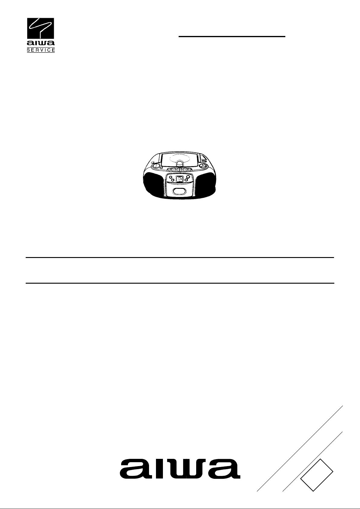
CSD-EX150
HR HC U2
SERVICE MANUAL
COMPACT DISC STEREO
RADIO CASSETTE RECORDER
MODEL CODE : 8ZCDB-0237(S)
This Service Manual is the "Revision Publishing" and replaces "Simple Manual"
(S/M Code No. 09-994-327-3T3).
BASIC TAPE MECHANISM : TN-21ZVC-1812
BASIC CD MECHANISM : DA-11T3C
S/M Code No. 09-994-327-3R3
REVISION
DATA
Page 2
SPECIFICATIONS
HR, HC MODELS
Design and specifications are subject to change without
•
notice
.
U2 MODEL
Design and specifications are subject to change without
•
notice
.
2
Page 3
PROTECTION OF EYES FROM LASER BEAM DURING SERVICING
This set employs laser. Therefore, be sure to follow carefully the
instructions below when servicing.
WARNING!
WHEN SERVICING, DO NOT APPROACH THE LASER EXIT
WITH THE EYE TOO CLOSELY. IN CASE IT IS NECESSARY TO
CONFIRM LASER BEAM EMISSION. BE SURE TO OBSERVE
FROM A DISTANCE OF MORE THAN 30cm FROM THE
SURFACE OF THE OBJECTIVE LENS ON THE OPTICAL
PICK-UP BLOCK.
Caution: Invisible laser radiation when
open and interlocks defeated avoid exposure to beam.
Advarsel:Usynling laserståling ved åbning,
når sikkerhedsafbrydere er ude af funktion.
Undgå udsættelse for stråling.
VAROITUS!
Laiteen Käyttäminen muulla kuin tässä käyttöohjeessa mainitulla tavalla saattaa altistaa käyt-täjän turvallisuusluokan 1 ylittävälle näkymättömälle lasersäteilylle.
VARNING!
Om apparaten används på annat sätt än vad som specificeras i
denna bruksanvising, kan användaren utsättas för osynling
laserstrålning, som överskrider gränsen för laserklass 1.
CAUTION
Use of controls or adjustments or performance of procedures
other than those specified herein may result in hazardous
radiation exposure.
ATTENTION
L'utilisation de commandes, réglages ou procédures autres que
ceux spécifiés peut entraîner une dangereuse exposition aux
radiations.
ADVARSEL!
Usynlig laserståling ved åbning, når sikkerhedsafbrydereer ude
af funktion. Undgå udsættelse for stråling.
This Compact Disc player is classified as a CLASS 1 LASER
product.
The CLASS 1 LASER PRODUCT label is located on the rear
exterior.
CLASS 1
KLASSE 1
LUOKAN 1
KLASS 1
LASER PRODUCT
LASER PRODUKT
LASER LAITE
LASER APPARAT
3
Page 4
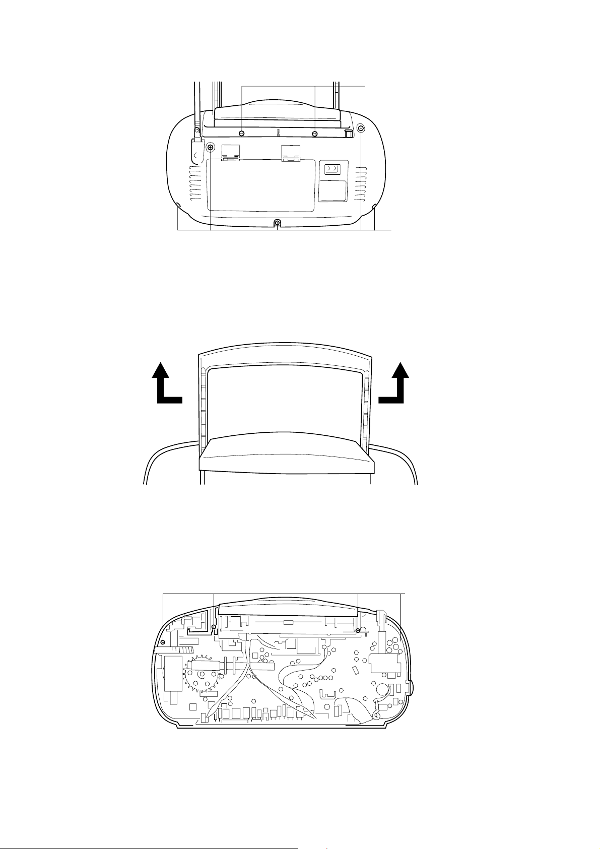
DISASSEMBLY INSTRUCTIONS
1. Remove the screws 1 (V+3-10 GLD*2), 2 (UT2+3-6*5) from the rear cabinet.
2. While pressing down the Q sound button, remove the rear cabinet .
Open the hanger wide to the right and left, and remove it.
1
2
3. Remove the screws 3 (V+3-10 GLD*4).
3
4
Page 5
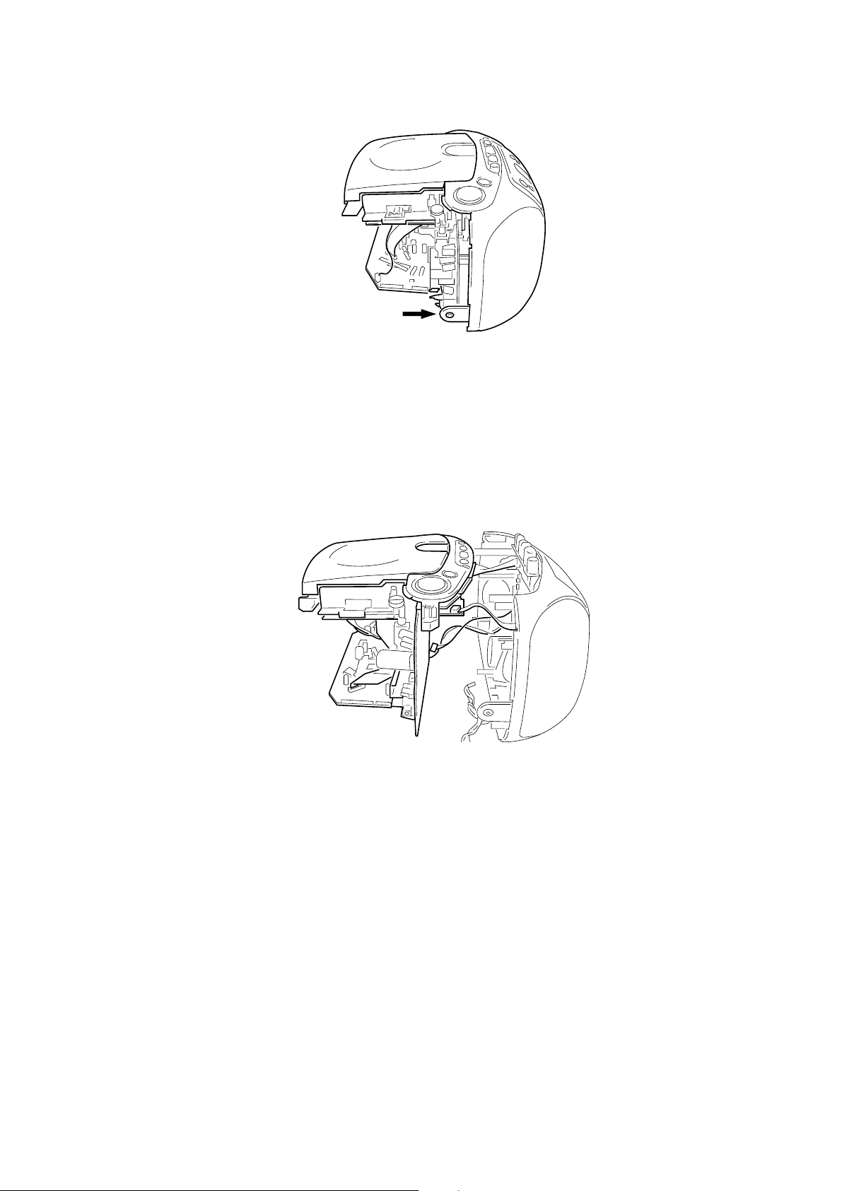
4. Put the part of front cabinet shown by the arrow away from the H.P jack
5. Remove the CD block, the main board, and others from the front cabinet.
5
Page 6

ELECTRICAL MAIN PARTS LIST
REF. NO PART NO. KANRI DESCRIPTION
NO.
IC
87-A20-955-010 IC,LA1828
87-070-416-010 IC,NJU7201 L55
87-A21-111-040 C-IC,M62495FP
87-A20-946-040 C-IC,MM1434XF
87-A21-193-010 IC,TA8227P
87-A21-145-040 C-IC,BA4560F-E2
87-A20-446-010 C-IC,LA9241ML
87-A20-459-010 C-IC,LC78622ED
87-A20-856-010 IC,BA6898S
8Z-CDB-651-010 C-IC,LC865516A-5L84
TRANSISTOR
89-319-233-080 TR,2SC1923 (0.1W)
87-026-572-080 TR,DTA114TS
87-026-215-080 TR,DTC114YS
87-026-291-080 TR,DTC124XS
89-318-154-080 TR,2SC1815 (0.4W)
89-113-184-080 TR,2SA1318T
89-112-965-080 TR,2SA1296 (0.75W)
87-026-463-080 TR,2SA933S (0.3W)
89-320-011-080 TR,2SC2001 (15W)
89-318-155-080 TR,2SC1815 (0.4W)
87-026-462-080 TR,2SC1740 S(RS 0.3W)
89-110-155-080 TR,2SA1015(0.4W)
87-026-496-080 FET,2SJ103GR
89-328-786-080 TR,2SC2878B
87-026-217-080 TR,DTC124ES
87-026-235-080 CHIP-TR,DTC114EK
87-026-211-080 TR,DTA144EK
87-026-447-080 TR,2SC1740S R
DIODE
87-020-465-080 DIODE,1SS133 (110MA)
87-017-162-080 ZENER,HZS7C3L
87-017-148-080 ZENER,HZS6A1L
87-070-136-080 ZENER,MTZJ5.1B
87-027-399-080 ZENER,HZ7A3L (200MA)<U>
87-027-607-080 ZENER,HZ7B3L<HR,HC>
87-017-139-010 ZENER,HZS15-2
87-A40-466-080 ZENER,MTZJ2.7A
87-A40-465-090 DIODE,FR202
MAIN C.B
C1 87-010-314-080 C-CAP,S 22P-50V
C2 87-010-316-080 C-CAP,S 33P-50 CH
C3 87-010-314-080 C-CAP,S 22P-50V
C5 87-010-151-080 C-CAP,S 7P-50 CH
C6 87-010-378-080 CAP, ELECT 10-16V
C7 87-018-208-080 CAP 0.047-50F
C8 87-010-197-080 CAP, CHIP 0.01 DM
C9 87-010-154-080 CAP CHIP 10P
C10 87-010-197-080 CAP, CHIP 0.01 DM
C12 87-010-314-080 C-CAP,S 22P-50V
C13 87-010-148-080 CAP, CHIP S 75P SL
C14 87-010-400-080 CAP, ELECT 0.47-50V
C15 87-010-197-080 CAP, CHIP 0.01 DM
C16 87-010-178-080 CHIP CAP 1000P
C17 87-016-669-080 C-CAP,S 0.1-25 K B
C18 87-016-460-080 C-CAP,S 0.22-16 B
C19 87-010-544-080 CAP, ELECT 0.1-50V
C20 87-010-400-080 CAP, ELECT 0.47-50V
C21 87-010-403-080 CAP, ELECT 3.3-50V
C22 87-010-197-080 CAP, CHIP 0.01 DM
C24 87-010-197-080 CAP, CHIP 0.01 DM<HR,HC>
C24 87-010-188-080 CAP,CHIP 6800P<U>
C25 87-010-197-080 CAP, CHIP 0.01 DM<HR,HC>
REF. NO PART NO. KANRI DESCRIPTION
NO.
C25 87-010-188-080 CAP,CHIP 6800P<U>
C26 87-016-460-080 C-CAP,S 0.22-16 B
C27 87-016-460-080 C-CAP,S 0.22-16 B
C28 87-010-194-080 CAP, CHIP 0.047
C29 87-010-194-080 CAP, CHIP 0.047
C30 87-010-248-080 CAP, ELECT 220-10V
C31 87-010-379-080 CAP, ELECT 22-16V
C32 87-010-197-080 CAP, CHIP 0.01 DM
C33 87-010-197-080 CAP, CHIP 0.01 DM
C34 87-010-197-080 CAP, CHIP 0.01 DM
C37 87-012-155-080 C-CAP 180P-50CH
C38 87-010-318-080 C-CAP,S 47P-50 CH
C91 87-010-197-080 CAP, CHIP 0.01 DM
C92 87-010-178-080 CHIP CAP 1000P
C97 87-018-134-080 CAPACITOR,TC-U 0.01-16<U>
C98 87-010-197-080 CAP, CHIP 0.01 DM<U>
C203 87-010-401-080 CAP, ELECT 1-50V
C204 87-010-221-080 CAP, ELECT 470-10V
C205 87-010-263-080 CAP, ELECT 100-10V
C206 87-010-248-080 CAP, ELECT 220-10V
C206 87-010-248-080 CAP, ELECT 220-10V
C210 87-010-198-080 CAP, CHIP 0.022
C211 87-010-260-080 CAP, ELECT 47-25V
C212 87-010-198-080 CAP, CHIP 0.022
C220 87-016-495-090 CAP,E 3300-25 SMG
C230 87-010-405-080 CAP, ELECT 10-50V
C231 87-010-404-080 CAP, ELECT 4.7-50V<HR,HC>
C232 87-010-263-080 CAP, ELECT 100-10V
C233 87-010-197-080 CAP, CHIP 0.01 DM
C234 87-010-263-080 CAP, ELECT 100-10V
C261 87-010-196-080 CHIP CAPACITOR,0.1-25
C262 87-010-384-080 CAP, ELECT 100-25V
C263 87-010-385-080 CAP, ELECT 220-25V
C264 87-010-196-080 CHIP CAPACITOR,0.1-25
C265 87-010-236-080 CAP,E 1000-10 SME
C301 87-010-405-080 CAP, ELECT 10-50V
C302 87-010-405-080 CAP, ELECT 10-50V
C303 87-010-405-080 CAP, ELECT 10-50V
C304 87-010-404-080 CAP, ELECT 4.7-50V
C305 87-010-213-080 C-CAP,S 0.015-50 B
C306 87-010-546-080 CAP, ELECT 0.33-50V
C307 87-010-544-080 CAP, ELECT 0.1-50V
C308 87-010-260-080 CAP, ELECT 47-25V
C309 87-010-263-080 CAP, ELECT 100-10V
C310 87-010-544-080 CAP, ELECT 0.1-50V
C311 87-010-546-080 CAP, ELECT 0.33-50V
C312 87-010-213-080 C-CAP,S 0.015-50 B
C313 87-010-404-080 CAP, ELECT 4.7-50V
C314 87-010-405-080 CAP, ELECT 10-50V
C315 87-010-405-080 CAP, ELECT 10-50V
C316 87-010-405-080 CAP, ELECT 10-50V
C317 87-010-401-080 CAP, ELECT 1-50V
C318 87-010-401-080 CAP, ELECT 1-50V
C319 87-010-197-080 CAP, CHIP 0.01 DM
C320 87-010-405-080 CAP, ELECT 10-50V
C321 87-010-260-080 CAP, ELECT 47-25V
C322 87-010-402-080 CAP, ELECT 2.2-50V
C325 87-010-400-080 CAP, ELECT 0.47-50V
C326 87-010-400-080 CAP, ELECT 0.47-50V
C329 87-010-401-080 CAP, ELECT 1-50V
C330 87-010-197-080 CAP, CHIP 0.01 DM
C331 87-010-197-080 CAP, CHIP 0.01 DM
C332 87-010-197-080 CAP, CHIP 0.01 DM
C333 87-010-197-080 CAP, CHIP 0.01 DM
C334 87-010-404-080 CAP, ELECT 4.7-50V
C335 87-010-401-080 CAP, ELECT 1-50V
C336 87-010-401-080 CAP, ELECT 1-50V
C337 87-010-178-080 CHIP CAP 1000P
C338 87-010-384-080 CAP, ELECT 100-25V
C339 87-010-404-080 CAP, ELECT 4.7-50V
6
Page 7

REF. NO PART NO. KANRI DESCRIPTION
NO.
C340 87-010-401-080 CAP, ELECT 1-50V
C341 87-010-178-080 CHIP CAP 1000P
C342 87-010-384-080 CAP, ELECT 100-25V
C343 87-010-384-080 CAP, ELECT 100-25V
C344 87-010-384-080 CAP, ELECT 100-25V
C345 87-010-384-080 CAP, ELECT 100-25V
C346 87-010-235-080 CAP,E 470-16 SME
C347 87-010-384-080 CAP, ELECT 100-25V
C348 87-010-235-080 CAP,E 470-16 SME
C351 87-010-401-080 CAP, ELECT 1-50V
C355 87-010-384-080 CAP, ELECT 100-25V
C401 87-010-178-080 CHIP CAP 1000P
C402 87-012-157-080 C-CAP,S 330P-50 CH
C403 87-012-157-080 C-CAP,S 330P-50 CH
C407 87-010-248-080 CAP, ELECT 220-10V
C410 87-010-402-080 CAP, ELECT 2.2-50V
C411 87-010-177-080 C-CAP,S 820P-50 SL
C412 87-010-402-080 CAP, ELECT 2.2-50V
C413 87-012-158-080 C-CAP,S 390P-50 CH
C415 87-010-406-080 CAP, ELECT 22-50
C416 87-010-404-080 CAP, ELECT 4.7-50V
C417 87-010-384-080 CAP, ELECT 100-25V
C418 87-010-402-080 CAP, ELECT 2.2-50V
C419 87-010-177-080 C-CAP,S 820P-50 SL
C420 87-012-158-080 C-CAP,S 390P-50 CH
C422 87-010-406-080 CAP, ELECT 22-50
C423 87-010-404-080 CAP, ELECT 4.7-50V
C424 87-010-194-080 CAP, CHIP 0.047
C425 87-010-177-080 C-CAP,S 820P-50 SL
C426 87-010-186-080 CAP,CHIP 4700P
C427 87-010-404-080 CAP, ELECT 4.7-50V
C428 87-010-260-080 CAP, ELECT 47-25V
C429 87-012-153-080 C-CAP,S 120P-50 CH
C430 87-010-213-080 C-CAP,S 0.015-50 B
C431 87-010-405-080 CAP, ELECT 10-50V
C433 87-010-177-080 C-CAP,S 820P-50 SL
C434 87-010-186-080 CAP,CHIP 4700P
C435 87-010-404-080 CAP, ELECT 4.7-50V
C436 87-012-153-080 C-CAP,S 120P-50 CH
C437 87-010-213-080 C-CAP,S 0.015-50 B
C438 87-010-405-080 CAP, ELECT 10-50V
C442 87-010-405-080 CAP, ELECT 10-50V
C445 87-010-194-080 CAP, CHIP 0.047
C490 87-010-322-080 C-CAP,S 100P-50 CH
C491 87-010-322-080 C-CAP,S 100P-50 CH
CF1 87-A90-128-010 FLTR,AM IF CFAL-455
CF2 82-785-747-080 CF,MS2 GHY,R
CF3 82-785-747-080 CF,MS2 GHY,R
CN210 87-049-919-010 CONN,3P EH V WHT
CN220 87-049-469-010 CONN,4P V
CN230 87-099-572-010 CONN,15P TUC-P15P-B1
CN320 87-049-469-010 CONN,4P V
CN330 87-009-031-010 CONNECTOR, 3P
CN410 87-049-469-010 CONN,4P V
CN420 87-009-030-010 CONNECTOR 2P PH M
D3 87-A40-226-080 VARI-CAP,SVC251SPA
J301 87-009-216-010 JACK, DIA 3.5
L2 87-A50-347-010 COIL,FM BPF EX<U>
L3 87-A50-350-010 COIL,BAR ANT AMN (COI)<HR,HC>
L3 87-A50-349-010 COIL,BAR ANT AMW (COI)<U>
L4 87-A50-345-010 COIL,FM RF EX
L5 87-A50-343-010 COIL,FM OSC EX<HR,HC>
L5 87-A50-449-010 COIL,FM OSC U<U>
L6 87-A50-337-010 COIL,AM OSC (TOKO)
L7 87-A50-336-010 COIL,AM IFT (TOKO)
L8 87-A50-335-010 COIL,FM IFT (TOKO)
L9 87-A50-334-010 COIL,FM DET (TOKO)
L10 87-003-102-080 COIL, 10UH
L310 87-003-098-010 COIL 2.2UH<U>
L401 87-007-342-010 COIL,OSC 85K BIAS
REF. NO PART NO. KANRI DESCRIPTION
PVC1 87-A91-318-010 TUN-CAP,20P-140P E(TWD)<HR,HC>
PVC1 87-A91-316-010 TUN-CAP,20P-160P U(TWD)<U>
S1 87-A91-174-010 SW,SL 2-4-2 SK42H01G06
S301 87-A90-815-010 SW,PUSH 2-2-6 SPUN19-S-501
S410 87-A91-173-010 SW,SL 2-2-3 SK23E01G04
CD C.B
C501 87-010-197-080 CAP, CHIP 0.01 DM
C502 87-010-221-080 CAP, ELECT 470-10V
C503 87-010-221-080 CAP, ELECT 470-10V
C504 87-010-197-080 CAP, CHIP 0.01 DM
C506 87-010-196-080 CHIP CAPACITOR,0.1-25
C507 87-010-196-080 CHIP CAPACITOR,0.1-25
C508 87-A10-381-080 CAP,E 1000-10 RE
C509 87-010-197-080 CAP, CHIP 0.01 DM
C510 87-010-197-080 CAP, CHIP 0.01 DM
C511 87-010-263-080 CAP, ELECT 100-10V
C513 87-010-196-080 CHIP CAPACITOR,0.1-25
C514 87-010-196-080 CHIP CAPACITOR,0.1-25
C515 87-012-157-080 C-CAP,S 330P-50 CH
C516 87-010-545-080 CAP, ELECT 0.22-50V
C525 87-010-176-080 C-CAP,S 680P-50 SL
C527 87-010-186-080 CAP,CHIP 4700P
C528 87-012-156-080 C-CAP,S 220P-50 CH
C529 87-010-545-080 CAP, ELECT 0.22-50V
C530 87-012-140-080 CAP 470P
C531 87-010-374-080 CAP, ELECT 47-10V
C532 87-010-401-080 CAP, ELECT 1-50V
C533 87-010-184-080 CHIP CAPACITOR 3300P(K)
C535 87-010-147-080 C-CAP,S 3P-50 CH
C536 87-010-314-080 C-CAP,S 22P-50 CH
C538 87-010-196-080 CHIP CAPACITOR,0.1-25
C539 87-010-404-080 CAP, ELECT 4.7-50V
C540 87-010-196-080 CHIP CAPACITOR,0.1-25
C541 87-010-405-080 CAP, ELECT 10-50V
C543 88-700-850-081 CAP, NYLAR 0.047
C544 88-700-920-810 CAP 0.15 MF50V
C545 87-010-197-080 CAP, CHIP 0.01 DM
C546 87-010-374-080 CAP, ELECT 47-10V
C547 87-010-263-080 CAP, ELECT 100-10V
C548 87-010-248-080 CAP, ELECT 220-10V
C549 87-010-198-080 CAP, CHIP 0.022
C550 87-010-374-080 CAP, ELECT 47-10V
C551 87-010-178-080 CHIP CAP 1000P
C552 87-010-197-080 CAP, CHIP 0.01 DM
C553 87-010-248-080 CAP, ELECT 220-10V
C554 87-010-263-080 CAP, ELECT 100-10V
C555 87-010-403-080 CAP, ELECT 3.3-50V
C556 87-010-197-080 CAP, CHIP 0.01 DM
C557 87-010-196-080 CHIP CAPACITOR,0.1-25
C558 87-010-197-080 CAP, CHIP 0.01 DM
C559 87-010-315-080 C-CAP,S 27P-50 CH
C560 87-010-263-080 CAP, ELECT 100-10V
C561 88-700-910-081 MYLAR,0.1
C562 87-010-196-080 CHIP CAPACITOR,0.1-25
C563 87-012-156-080 C-CAP,S 220P-50 CH
C564 87-018-121-080 CAP, CER 150P-50V
C565 87-010-263-080 CAP, ELECT 100-10V
C566 87-010-196-080 CHIP CAPACITOR,0.1-25
C569 87-010-404-080 CAP, ELECT 4.7-50V
C570 87-018-134-080 CAPACITOR,TC-U 0.01-16<U>
C571 87-010-248-080 CAP, ELECT 220-10V
C572 87-010-196-080 CHIP CAPACITOR,0.1-25
C573 87-010-196-080 CHIP CAPACITOR,0.1-25
C575 87-010-312-080 C-CAP,S 15P-50 CH
C576 87-010-312-080 C-CAP,S 15P-50 CH
C578 87-018-134-080 CAPACITOR,TC-U 0.01-16
C579 87-010-263-080 CAP, ELECT 100-10V
C582 87-010-196-080 CHIP CAPACITOR,0.1-25
NO.
7
Page 8

REF. NO PART NO. KANRI DESCRIPTION
NO.
C583 87-010-405-080 CAP, ELECT 10-50V
C584 87-012-156-080 C-CAP,S 220P-50 CH
C585 87-010-405-080 CAP, ELECT 10-50V
C586 87-012-156-080 C-CAP,S 220P-50 CH
C587 87-010-322-080 C-CAP,S 100P-50 CH
C589 87-010-322-080 C-CAP,S 100P-50 CH
C590 87-010-322-080 C-CAP,S 100P-50 CH
C591 87-010-322-080 C-CAP,S 100P-50 CH
C592 87-010-322-080 C-CAP,S 100P-50 CH
C593 87-010-196-080 CHIP CAPACITOR,0.1-25
C601 87-010-313-080 CAP, CHIP 18P
C602 87-010-313-080 CAP, CHIP 18P
C603 87-010-197-080 CAP, CHIP 0.01 DM
C604 87-010-196-080 CHIP CAPACITOR,0.1-25
C605 87-010-385-080 CAP, ELECT 220-25V
C611 87-010-401-080 CAP, ELECT 1-50V
C612 87-010-400-080 CAP, ELECT 0.47-50V
C640 87-010-197-080 CAP, CHIP 0.01 DM
C641 87-010-197-080 CAP, CHIP 0.01 DM
C644 87-018-134-080 CAPACITOR,TC-U 0.01-16
C655 87-010-178-080 CHIP CAP 1000P
C656 87-015-627-080 C-CAP,1000P-50 B
C657 87-010-197-080 CAP, CHIP 0.01 DM
C658 87-015-819-080 CAPACITOR,0.01
C659 87-010-178-080 CHIP CAP 1000P
C660 87-010-405-080 CAP, ELECT 10-50V
C685 87-010-317-080 C-CAP,S 39P-50 CH
C686 87-010-319-080 C-CAP,S 56P-50 CH
C690 87-010-312-080 C-CAP,S 15P-50 CH
CN520 87-A60-424-010 CONN,16P V TOC-B
CN610 87-099-751-010 CONN,16P V 9604SC
CN630 87-009-030-010 CONNECTOR 2P PH M
CN640 87-099-561-010 CONN,15P TUC-P15X-B1
L501 87-003-102-080 COIL, 10UH
L502 87-003-226-080 MICRO INDUCTOR 100UJ
L504 87-003-102-080 COIL, 10UH
L505 87-003-226-080 MICRO INDUCTOR 100UJ<U>
L590 87-003-102-080 COIL, 10UH<U>
L591 87-008-372-010 FILTER, EMI BL OIRNI<U>
L592 87-003-226-080 MICRO INDUCTOR 100UJ
L593 87-003-102-080 COIL, 10UH<U>
L601 87-003-143-080 COIL 4.7 UH
L602 87-008-372-010 FILTER, EMI BL OIRNI
SFR501 87-024-176-080 SEMI-FIXED RESISTOR, 100K
X501 81-592-641-080 CERALOCK 16.93MHZ
X601 87-030-273-010 VIB,XTAL 32.768K5PPM
X602 87-030-376-080 VIB,CER CSA5.76MG200
REF. NO PART NO. KANRI DESCRIPTION
FRONT C.B
CN620 87-099-757-010 CONN,16P 9604S F
D601 87-A91-172-010 LED, SA36-11HWA-11.0MM RED
D611 87-A40-622-010 LED,L-34HDSL RED
D614 87-A40-622-010 LED,L-34HDSL RED
S601 87-A90-164-080 SW,TACT SKQAB(N)
S602 87-A90-164-080 SW,TACT SKQAB(N)
S603 87-A90-164-080 SW,TACT SKQAB(N)
S604 87-A90-164-080 SW,TACT SKQAB(N)
S605 87-A90-164-080 SW,TACT SKQAB(N)
KEY L C.B
D641 87-A40-623-010 LED,L-34GDSL GRN
D642 87-A40-623-010 LED,L-34GDSL GRN
S606 87-A90-164-080 SW,TACT SKQAB(N)
S607 87-A90-164-080 SW,TACT SKQAB(N)
S608 87-A90-164-080 SW,TACT SKQAB(N)
KEY R C.B
S611 87-A90-164-080 SW,TACT SKQAB(N)
S620 87-A90-164-080 SW,TACT SKQAB(N)
S621 87-A90-164-080 SW,TACT SKQAB(N)
MOTOR C.B
M2 9X-262-576-910 MOTOR GEAR ASSY
PIN3 91-564-722-110 CONNECTOR 6P
SW1 91-572-085-120 LEAF SW
AC C.B
C901 87-A11-132-080 CAP,TC U 0.01-50 K B
C902 87-A11-132-080 CAP,TC U 0.01-50 K B
C903 87-A11-132-080 CAP,TC U 0.01-50 K B
C904 87-A11-132-080 CAP,TC U 0.01-50 K B
CN910 87-049-919-010 CONN,3P EH V WHT
!
F901 87-A90-092-080 PROTECTOR,2.5A 491<HR,HC>
NO.
8
Page 9
• Regarding connectors, they are not stocked as they are not the initial order items.
The connectors are available after they are supplied from connector manufacturers upon the order is received.
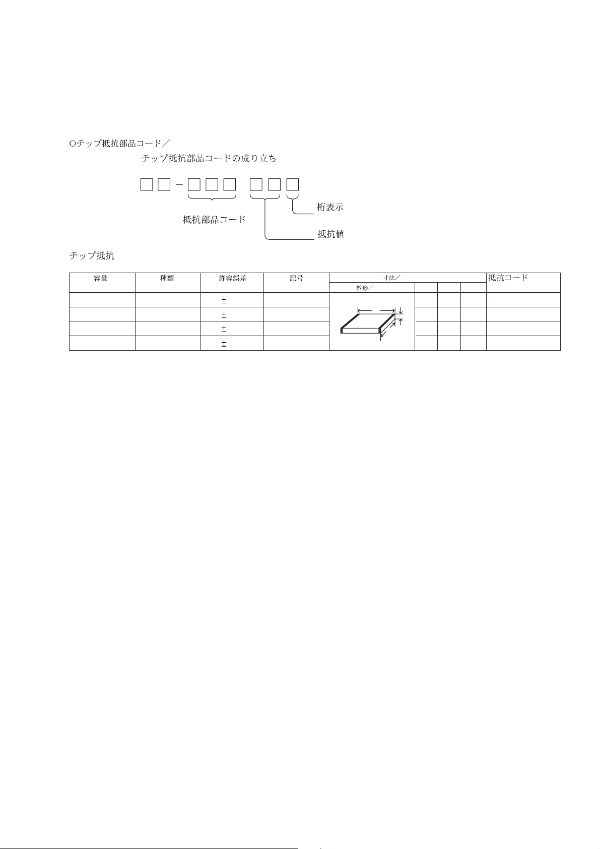
CHIP RESISTOR PART CODE
Chip Resistor Part Coding
88
A
Resistor Code
Chip resistor
Wattage Type Tolerance
1/16W 1005 5% CJ
1/16W
1/10W
1/8W
1608
2125
3216
5%
5%
5%
Symbol
CJ
CJ
CJ
Figure
Value of resistor
Form
L
Dimensions (mm)
t
W
0.55
Resistor Code
108
118
128
LW t
1.0 0.5 0.35 104
1.6 0.8 0.45
2 1.25 0.45
3.2
1.6
: A
: A
9
Page 10
TRANSISTOR ILLUSTRATION
E C B
E C B
B C E
S G D
C
E
B
2SA933
2SC1740
DTA144EK
DTA114TS
DTC114YS
DTC124XS
2SA1015
2SA1296
2SA1318
2SC1815
2SC1923
2SC2001
2SC2878
2SB1370
2SJ103
DTC114EK
10
Page 11

IC BLOCK DIAGRAM
IC, LA1828
IC, TA8227P
IC, MM1434XF
IC, BA6898S
1211
Page 12

WIRING-1 (MAIN)
1
234567
8
9
10
11 12 13
14
KEY L C.B (INSERTED PARTS) KEY R C.B (INSERTED PARTS)
A
S606,D642
CD
S607,D641
RADIO
B
C
D
S001
BAND
FM AM
L3
AM ANTENNA
S608
TAPE
EH
RPH
LR
1
PN410
SW420
REC
SW
4
1
4
5
8
1
2
2
1
1
510
20
24
1
2
S611
3 - MODE
EQUALIZER
TO/FROM
CD C. B CN540
12
15
13
S621
VOL
S620
VOL
S301
Q SOUND
OFF
ON
1346
1
8
5
10
9
16
7 9 10 12
E
F
G
H
S410
FM MODE/OSC
STEREO
MONO
U MODEL
ANT - FM
BATT C.B
24 20 15 13
1 5 10 12
U MODEL
BATTERY
R14 x 8
DC12V
1
4
8
5
MAIN C.B (INSERTED PARTS)
POWER C.B
1 5 10 15
TO/FROM CD C. B
CN640
EXCEPT HR, HC MODEL
PT901
U MODEL
HR, HC MODEL
2
1
3
J601
AC
HR, HC MODEL
M1
DECK
MOTOR
1 PN220
M
4
3
2
1
4
S1
DECK
SW
J301
1PN3204
SP1
L CH
SP2
R CH
I
PT901
J
U MODEL
EXCEPT U MODEL
HR, HC MODEL
SW 901
2
1
3
AV VOLTAGE
AC110V - 120V AC220V
120V AC240V
J601
AC
1413
Page 13

14
13 12 11 10 9 8
KEY R C.B (CHIP PARTS) KEY L C.B (CHIP PARTS)
7
6
5
432
1
A
B
C
D
U MODEL:L310
EXCEPT
U MODEL:JW330
U MODEL
E
U MODEL
F
G
MAIN C.B (CHIP PARTS)
H
I
J
1615
Page 14

SCHEMATIC DIAGRAM-1 (MAIN 1/2)
TO/FROM CD C. B (2/2) CN640
SW420
REC
SW
CN420
KEY L C. B
KEY R
C. B
RADIO
CD
R
3-MODE
EQJALIZER
V
V
10k
Q420, 421
PB SWITCH
R
LED DRIVELED DRIVE
CD
RADIO
TAPE B + SWITCH
PB AMP
D490
1N4148
Q409, 410
TAPE B + SWITCH
(1/2)
MAIN C. B (1/2)
TO/FROM MAIN C.B (2/2)
Q207, 206
TU B + SWITCH
1N4148
TO/FROM CD C.B (1/2) CN540
S301
QSOUND
ON
OFF
IC302
Q-SOUND
EQ AMP
U
4.7k
4.7k
IC301
AUDIO SELECT/AMP
U
J301
PN320
(L)
(R)
MUTE
MUTE
IC303
AF
POWER
AMP
R
L
RPH
AZIMU TH
ADJ.
EH
R486
Q430,431,432,433
BIAS SWITCH
PN410
R485
10k
R999
C445
BIAS OSC
10k
0.047µF
6.8k
4.7k
IC260
5.3V REG
Q222,223
AC IN DETECT
7.8V
5.5V REG
5.5V
REG
7.8V
REG
Q226
R
LED
DRIVER
5.6
SWITCH
2SD1370
8:
81
82
83
84
87
REG
U HR, HC
2.2k
HZ7A3L
MOUNT
NO MOUNT
NO MOUNT
R
4.7k
HZ7B3L
NO MOUNT
MOUNT
4.7/50V
M1
DECK
MOTOR
R
Q270,271
MOTOR
DRIVE/SWITCH
TAPE MECHA BLOCK
10k
DECK
SW
S1
87
R
PN220
Q210,211
201
B + SWITCH
U
EXCEPT U
POWER
C. B
4
10V
REG
BATT
R14 x 8
BATT C. B
AC VOL TAGE
HR, HC MODEL
AC120V 60Hz
AC~
AC~
AC~
SIGNAL
: FM / PB
: AM / REC
C490
100P
D492
D493
1N4148
2SA933S
D491
1N4148
C491
100P
R491
5.6k
R492
CN410
22k
4.7k
D420
IN4148
D421
S410
FM MODE/OSC
STEREO
MONO
IN4148
56
56
5.6k
(1/2)
(1/2)
PB AMP
REC AMP
REC AMP
Q406,407,408
REC SWITCH
(2/2)
(2/2)
(2/2)
L401,C404
AC BIAS
ADJ.
Q402,403 BIAS LEVEL SWITCH
1817
Page 15

SCHEMATIC DIAGRAM-2 (MAIN 2/2)
PVC001A
MAIN C.B (2/2)
CT1C
CT1D
8
75P
Q 2.3
SWITCH
R
R
FM IF ADJ
BAND
FM AM
S410
FM MODE/OSC
FM IF ADJ.
AM IF ADJ.
FM FREQ.
RANGE ADJ.
AM FREQ. RANGE.
ADJ
STEREO
MONO
(2/2)
TO/FROM
MAIN C.B (1/2)
IF AMP
L6,CT1B
CT1B
CT1A
L3
L5, CT1D
FM TRACKING ADJ.
L4, CT1C
TUNING
PVC 1
AM TRACKING ADJ.
L3, CT1A
PVC1A - 1D
CT1A - 1D
AM/FM FRONTEND
SIGNAL
: FM / PB
: AM / REC
HC, HR U
C024/C025
L005
R004
R091
C098
C097
PVC001
8 : 8 :
0.01uF
5 1/2T 3.3MM
10
NM
NM
NM
140P
6800P
6 1/2T 3.0MM
(WITH SHIELD
CASE)
22
4.7k
0.01uF
0.01uF
160P
HC, HR U
L002
NM
2 1/2T 5.0MM
7P
C005
0.01uF
C002
33P
C003
22P
C092
1000P
C038
47P
C091
D003
SVC251SPA
2019
Page 16

WIRING-2 (CD)
FRONT C. B
CD C. B (INSERTED PARTS)
E
TO/FROM MAIN C. B CN230
15
10 15
D
48
64 1
33
33
32
U MODEL
16
17
49
48
C
B
MOTOR C.B
TO/ FROM MAIN C. B
CN330
1
3
16 10 5 1
17 20 25 30 32
A
1
1
234567
234567
CD C. B (CHIP PARTS)
49
32
64
1
17
16
1
48
PICK UP ASSY
SF-P101 NR
8
8
37
16
15
2
1
36
9
9
12
13
25
24
2
1
1
PN630
2
SW630
DOOR
10
SW
10
11 12 13
11 12 13
(INSERTED PARTS)
15
1016
125
S601
REPEAT
S603
D601
CD TRACK
D611
OP/BATT
D614
REPEAT
S602
STOP/
MEMORY
S605
PLAY/
PAUSE
FRONT C. B
(CHIP PARTS)
S604
14
14
A
B
C
D
E
2221
Page 17

SCHEMATIC DIAGRAM-3 (CD 1/2)
CD C.B (1/2)
CD MECHANISM
DA-11T3C
OPTICAL PICK UP
BLOCK SF-P101 NR
1N4148
LED
DRIVER
C544 0.33/50
C543 M0.047
TO/FROM CD C.B (2/2)
CN1
CN520
120k
120k
120k
120k
150k
150k
3.9k
0.01
4.7k
22P
1k
3P
C535
JW
4700P
47k
F.B
100uH
47k
D510
1N4148
D511
1N4148
Q501,502
B + SWITCH
IC502
LC78622ED
10uH
8
TO/FROM CD C.B (2/2)
MOTOR C.B
M1
M2
SW1
PIN3
CN510
IC503
SPINDOLE/
SLED
MOTOR
DRIVER
REG
8:
C570 0.01uH NM
8
U
TO/FROM MAIN CD C.B (1/2) CN330
R
EXCEPT U
SIGNAL
: FM / PB
: AM / REC
2423
Page 18

SCHEMATIC DIAGRAM-4 (CD 2/2)
TO/FROM CD C.B (1/2)
FRONT C. B
REPEAT
LED DEIVER
1.5k
RR
SEGMENT
DRIVER
1.5k
1.5k
1.5k
1.5k
OP/BATT
CD C.B (2/2)
1000P
1000P
1000P
1000P
1000P
1000P
1000P
1000P
P
TO/FROM MAIN CD C.B (1/2) CN230
SYSTEM CONTROL
SW630
(DOOR SW)
CN640
CD TRACK
S605 S604 S603 S602 S601
PLAY/
PAUSE
STOP/
MEMORY
REPEAT
CLOCK SHIFT SWITCH
R
Q690
L651
Q603,604,602
RESET
TO/FROM MAIN CD C.B (1/2) CN230
R
2625
Page 19

ELECTRICAL ADJUSTMENT
MAIN C.B
2
1
2
5
L3
L401
CT1A
L4
L8
CT1C
L6
CT1B
CT1D
L5
L7
L9
6364 7
8
< RADIO SECTION >
1. AM Frequency Range Adjustment
L6 ...................................................................... 517±3kHz
CT1B .............................................................. 1750±10kHz
2. AM Tracking Adjustment
L3 .......................................................................... 600kHz
CT1A.................................................................... 1400kHz
3. AM IF Adjustment
L7 .......................................................................... 455kHz
4. FM Frequency Range Adjustment
L5 ................................................................... 87±0.3MHz
CT1D............................................................. 109±0.3MHz
5. FM Tracking Adjustment
L4 ...........................................................................88MHz
CT1C .....................................................................108MHz
6. FM IF Adjustment
L8, L9 ...................................................................10.7MHz
< TAPE RECORDER SECTION >
7. Bias Adjustment
L401 ......................................................................... 60kHz
8. Azimuth Adjustment
Condition: • Test tape: TTA-320
• Test point: PHONES JACK
• Adjustment location:Azimuth adjustment
screw
Method: Play back the test tape and adjust so that the
output is maximum.
27
Page 20

PRACTICAL SERVICE FIGURE
< FM SECTION >
IHF Sensitivity: Less than 20dB
(THD 3%)
Signal to noise ratio: More than 55dB
(Input 54dB) (at 98.0MHz)
Distortion: Less than 2.0% (at 98.0MHz)
(Input 54dB) Less than 5.0% (at 98.0MHz)
Stereo separation: More than 18dB (at 98.0MHz)
Intermediate frequency: 10.7±0.1MHz
< AM SECTION >
Sensitivity:
(S/N 10dB) Less than 45dB
Signal to noise ratio: More than 34dB
(Input 74dB)
Distortion: Less than 1.5%
(Input 74dB) (at 1000kHz)
Intermediate frequency: 455kHz
< DECK SECTION >
Tape speed: 3000Hz±2%
Distortion: Less than 2.0% (PB)
Less than 2.5% (REC)
Signal to noise ratio: More than 44dB (AC)
More than 50dB (DC)
Erasing ratio: More than 45dB
28
Page 21

IC DESCRIPTION
IC, LC865508A
Pin No. Pin Name I/O Description
1
2
3
O-SEG E
______________
O-SEG F
_______________
O-SEG G
O
O
O
SEG E control.
SEG F control.
SEG G control.
10
11
12
13
14
15
16
17
18
19
20
21
22
4
5
6
7
8
9
—
I-RST
XT1 (IN)
NC
XT2 (OUT)
VSS
CF1 (IN)
CF2 (OUT)
VDD
I-KEY0
I-KEY1
I-DECK
____________
I-CD SW
O-CLK SFT
NC
O-BASS LED
O-Qsound LED
O-SFT LED
I-DRF
—
—
—
—
—
Not used.
I
Microprocessor reset input.
I
Connected to an external 32.768 kHz crystal oscillator.
Not used.
O
Connected to an external 32.768 kHz crystal oscillator.
GND.
I
Connected to an external 5.76 MHz ceramic filter.
O
Connected to an external 5.76 MHz ceramic filter.
Microprocessor power supply (+5 V).
I
Key AD input. (AD)
I
Key AD input. (AD)
I
Deck status input. (AD)
I
CD door switch status input.
O
Main clock shift output.
Not used.
O
BASS LED ON/OFF control output.
O
Q sound LED ON/OFF control output.
O
Clock shift A standby input.
I
CD RF level detection input.
23
24
25
26
27
28
29
30
31
32
33
34
35
36
37
38
39
40
I-WRQ
NC
I-REMO
O-CD ON
O-TU ON
O-P.CONT
NC
O-Qsound CONT
O-MUTE
O-DIGIT
O-RP LED
O-COIN
I-SQOUT
O-CQCK
O-RWC
O-DATA
O-CD FUNC LED
O-TU FUNC LED
—
—
I
CD subcode Q standby input.
Not used.
I
Remote control input.
O
CD power control output.
O
TU power control output.
O
The main power supply control output.
Not used.
O
Q sound ON/OFF control output.
O
Main mute output.
O
7-segment LED power supply control output.
O
REPEAT LED ON/OFF control output.
O
CD command output.
I
CD subcode Q input.
O
CD command/CLK for subcode.
O
CD read/write control output.
O
Data output to M62439FP.
O
LED ON/OFF control output for the CD function
O
LED ON/OFF control output for the TU function
41
O-TA FUNC LED
O
LED ON/OFF control output for the TA function
29
Page 22

Pin No. Pin Name I/O Description
42
43
44
NC
O-SEG DP
O-SEG A
—
O
O
Not used.
SEG DP control.
SEG A control.
45
46
47
48
O-SEG B
O-SEG C
O-SEG D
NC
—
O
O
O
SEG B control.
SEG C control.
SEG D control.
Not used.
30
Page 23

IC, LA9241ML
Pin No. Pin Name I/O Description
1
2
FIN2
FIN1
Pin to which external pickup photo diode is connected. RF signal is created by adding
I
with the FIN1 pin signal. FE signal is created by subtracting from the FIN1 pin signal.
I
Pin to which external pickup photo diode is connected.
10
11
12
13
14
15
16
17
3
4
5
6
7
8
9
E
F
TB
TE–
TE
TESI
SCI
TH
TA
TD–
TD
JP
TO
FD
FD–
Pin to which external pickup photo diode is connected. TE signal is created by
I
subtracting from the F pin signal.
I
Pin to which external pickup photo diode is connected.
I
DC component of the TE signal is input.
I
Pin to which external resistor setting the TE signal gain is connected between the TE pin.
O
TE signal output pin.
TES “Track Error Sense” comparator input pin. TE signal is passed through a band-
I
pass filter then input.
I
Shock detection signal input pin.
I
Tracking gain time constant setting pin.
O
TA amplifier output pin.
Pin to which external tracking phase compensation constants are connected between
I
the TD and VR pins.
I
Tracking phase compensation setting pin.
I
Tracking jump signal (kick pulse) amplitude setting pin.
O
Tracking control signal output pin.
O
Focusing control signal output pin.
Pin to which external focusing phase compensation constants are connected between
I
the FD and FA pins.
18
19
20
21
22
23
24
25
26
27
28
29
30, 31
32, 33
34
FA
FA–
FE
FE–
AGND
NC
SP
SPG
SP–
SPD
SLEQ
SLD
SL–, SL+
JP–, JP+
TGL
—
—
Pin to which external focusing phase compensation constants are connected between
I
the FD– and FA– pins.
Pin to which external focusing phase compensation constants are connected between
I
the FA and FE pins.
O
FE signal output pin.
I
Pin to which external FE signal gain setting resistor is connected between the FE pin.
Analog signal GND.
No connection.
O
Single ended output of the CV+ and CV– pin input signal.
I
Pin to which external spindle gain setting resistor in 12 cm mode is connected.
Pin to which external spindle phase compensation constants are connected together
I
with SPD pin.
O
Spindle control signal output pin.
I
Pin to which external sled phase compensation constants are connected.
O
Sled control signal output pin.
I
Sled advance signal input pin from microprocessor.
I
Tracking jump signal input pin from DSP.
I
Tracking gain control signal input from DSP. Low gain when TGL = H.
35
TOFF
I
Tracking off control signal input pin from DSP. Off when TOFF = H.
31
Page 24

Pin No. Pin Name I/O Description
36
TES
O
Pin from which TES signal is output to DSP.
37
38
39, 40
41
42
43
44
45
46
47
48
49
50
51
52
53
54
55
HFL
SLOF
CV–, CV+
RFSM
RFS–
SLC
SLI
DGND
FSC
TBC
NC
DEF
CLK
CL
DAT
CE
DRF
FSS
—
—
“High Frequency Level” is used to judge whether the main beam position is on top of
O
bit or on top of mirror.
I
Sled servo off control input pin.
I
CLV error signal input pin from DSP.
O
RF output pin.
RF gain setting and EFM signal 3T compensation constant setting pin together with
I
RFSM pin.
“Slice Level Control” is the output pin which controls the RF signal data slice level by
O
DSP.
I
Input pin which control the data slice level by the DSP.
Digital system GND.
O
Output pin to which external focus search smoothing capacitor is connected.
I
“Tracking Balance Control” EF balance variable range setting pin.
No connection.
O
Disc defect detector output pin.
I
Reference clock input pin. 4.23 MHz of the DSP is input.
I
Microprocessor command clock input pin.
I
Microprocessor command data input pin.
I
Microprocessor command chip enable input pin.
O
“Detect RF” RF level detector output.
I
“Focus Search Select” focus search mode (± search/+ search) select pin.
56
57
58
59
60
61
62
63
64
VCC2
REFI
VR
LF2
PH1
BH1
LDD
LDS
VCC1
—
—
—
Servo system and digital system Vcc pin.
Pin to which external bypass capacitor for reference voltage is connected.
O
Reference voltage output pin.
I
Disc defect detector time constant setting pin.
I
Pin to which external capacitor for RF signal peak holding is connected.
I
Pin to which external capacitor for RF signal bottom holding is connected.
O
APC circuit output pin.
I
APC circuit input pin.
RF system Vcc pin.
32
Page 25

IC, LC78622ED
Pin No. Pin Name I/O Description
1
2
3
4
DEFI
TAI
PDO
VVSS
I
Defect sense signal (DEF) input pin. (Connect to 0V when not used).
I
O
—
Test signal input pin with built-in pull-down resistor. Be sure to connect to 0V.
Phase comparator output pin to control external VCO.
GND pin for built-in VCO. Be sure to connect to 0V.
For PLL.
5
6
7
8
9
ISET
VVDD
FR
VSS
EFMO
I
—
I
—
Digital system GND. Be sure to connect to 0V.
O
Pin to which external resistor adjusting the PD0 output current.
Power supply pin for built-in VCO.
Pin for VCO frequency range adjustment.
EFM signal output pin.
For slice level control.
10
11
12, 13
14
EFMIN
TEST2
CLV+, CLV–
___
V/P
I
I
Test signal input pin with built-in pull-down resistor. Be sure to connect to 0V.
O
Disc motor control output. Three level output is possible using command.
Rough servo or phase control automatic selection monitoring output pin. Rough servo
O
EFM signal input pin.
at H. Phase servo at L.
15
16
17
18
19, 20
21
22
HFL
TES
TOFF
TGL
JP+, JP–
PCK
FSEQ
I
Track detect signal input pin. Schmidt input.
I
Tracking error signal input pin. Schmidt input.
O
Tracking OFF output pin.
O
Tracking gain selection output pin. Gain boost at L.
O
Track jump control signal output pin. Three level output is possible using command.
O
EFM data playback clock monitoring pin 4.3218 MHz when phase is locked in.
Sync signal detection output pin. H when the sync signal which is detected from EFM
O
signal and thesync signal which is internally generated agree.
23
VDD
—
Digital system power supply pin.
The pin is controlled by the serial data
command from microprocessor. When
24-28
SL+ - PUIN
I/O
General purpose input/output pin 1 to 5.
the pin is not used, set the pin to the input
terminal and connect to 0V, or alternately
set the pin to output terminal and leave
the pin open.
29
EMPH
O
De-emphasis monitor output pin. De-emphasis disc is being played back at H.
Pin No. Pin Name I/O Description
43
44
45
46
47
48
49
50
XVDD
XOUT
XIN
XVSS
SBSY
EFLG
PW
SFSY
—
Crystal oscillator power supply pin.
O
Pin to which external 16.9344 MHz crystal oscillator is connected.
I
—
Crystal oscillator GND pin. Be sure to connect to 0V.
O
Subcode block sync signal output pin.
O
C1, C2, single and dual correction monitoring pin.
O
Subcode P, Q, R, S, T, U and W output pin.
O
Subcode frame sync signal output pin. Falls down when subcode enters standby.
Subcode read clock input pin. Schmidt input. (Be sure to connected to 0V when not
51
SBCK
I
in use.)
52
FSX
Pin outputting the 7.35 kHz sync signal which is generated by dividing frequency of
O
crystal oscillator.
53
54
55
56
57
58
59
60
61
62
63
WRQ
RWC
SQOUT
COIN
___________
CQCK
________
RES
TST11
16M
4.2M
TEST5
______
CS
O
Subcode Q output standby output pin.
I
Read/write control input pin. Schmidt input.
O
Subcode Q output pin.
I
Command input pin from microprocessor.
I
Command input read clock or subcode read input clock from SQOUT pin
I
LC78622 reset input pin. Set this pin to L once when the main power is turned on.
O
Test signal output pin. Use this pin as open (normally L output).
O
16.9344 MHz output pin.
O
4.2336 MHz output pin.
I
Test signal input pin with built-in pull-down resistor. Be sure to connect to 0V.
Chip select signal input pin with built-in pull-down resistor. Be sure to connect to 0V
I
while it is not controlling.
64
TEST1
I
Test signal input pin without built-in pull-down resistor. Be sure to connect to 0V.
Note: The same potential must be applied to the respective power supply terminals. (VDD, VVDD, LVDD, RVDD, XVDD)
30
31
32, 33
34
35
36
37
38
39
40
41
42
C2F
DOUT
TEST3, TEST4
N.C.
MUTEL
LVDD
LCHO
LVSS
RVSS
RCHO
RVDD
MUTER
O
C2 flag output pin.
O
DIGITAL OUT output pin. (EIAJ format).
I
Test signal input pin with built-in pull-down resistor. Be sure to connect to 0V.
—
Not used. Set the pin to open.
O
—
L-channel 1-bit DAC.
O
—
—
O
L-channel mute output pin.
L-channel power supply pin.
L-channel output pin.
L-channel GND. Be sure to connect to 0V.
R-channel GND. Be sure to connect to 0V.
R-channel output pin.
R-channel 1-bit DAC.
—
O
R-channel power supply pin.
R-channel mute output pin.
3433
Page 26

MECHANICAL EXPLODED VIEW 1/1
40
A
A
38
G
A
43
C
48
P.C.B
E
46
44
G
41
A
65
66
A
A
C
A
49
P.C.B
WIRE ASSY,FM-ANT
42
HLDR,BAR ANT
63
A
50
62
47
51
A
C
A
C
52
53
54
56
B
60
61
55
57
58
59
34
33
22
23
24
25
26
D
1
4
2
3
6
69
32
35
12
16
13
64
F
F
A
17
18
19
20
A
21
A
A
31
A
30
29
14
37
45
15
28
27
A
5
P.C.B
A
A
7
D
68
A
A
DA11T3C
67
TN-21ZVC1812
A
36
15
39
70
PLATE,COVER
PT
P.C.B
A
67
A
13
10
8
9
11
12
P.C.B
A
3635
Page 27

MECHANICAL PARTS LIST 1/1
REF. NO PART NO. KANRI DESCRIPTION
1 84-CD8-083-010 BADGE,AIWA 30.5-5.2 2.5LEAD
2 8Z-CDB-004-010 WINDOW,LED(EX)<HR,HC>
2 8Z-CDB-046-010 WINDOW,LED(U)<U>
3 8Z-CDB-042-010 PANEL,FRONT(U)
4 8Z-CDB-026-010 KEY,CD A
5 8Z-CDB-027-010 KEY,CD B
6 8Z-CDB-625-010 FF-CABLE, 16P 1.25 240MM FRONT
7 8Z-CDB-012-010 GRILLE,SPKR L<U>
7 8Z-CDB-095-010 GRILLE,SPKR R (GRAY)<HR,HC>
8 8Z-CDB-006-010 LID,CASS
9 8Z-CDB-210-010 SPR-T,LID CASS
10 8Z-CDB-008-010 WINDOW,CASS
11 8Z-CDB-094-010 GRILLE,SPKR L (GRAY)<HR,HC>
11 8Z-CDB-013-010 GRILLE,SPKR R<U>
12 84-CD5-216-010 BRACKET
13 84-CD5-215-010 GEAR
14 8Z-CDB-001-010 CABI,FRONT
15 88-CD8-622-010 SPKR,F 77 7OHM 3W
16 8Z-CDB-019-010 KEY,CASS PAUSE
17 8Z-CDB-021-010 KEY,CASS STOP
18 8Z-CDB-022-010 KEY,CASS FF
19 8Z-CDB-023-010 KEY,CASS REW
20 8Z-CDB-020-010 KEY,CASS PLAY
21 8Z-CDB-018-010 KEY,CASS REC
22 84-CT5-209-010 PLATE,MAGNET
23 87-036-368-010 MAGNET
24 8Z-CDB-215-010 HLDR,LID CD
25 8Z-CDB-170-010 BASE,CHUCK
26 88-CD9-211-010 RING,CHUCK
27 87-CD7-207-010 HLDR,LOCKER
28 82-CD8-212-010 SPR-T,CAM CD
29 87-CD7-206-010 DOOR,CD LOCKER
30 8Z-CDB-025-010 KEY,EQ
31 8Z-CDB-016-010 KEY,VOL
32 8Z-CDB-047-010 CHAS,CD(U)
33 8Z-CDB-009-010 WINDOW,CD
34 8Z-CDB-005-010 LID,CD
35 8Z-CDB-211-010 SPR-T,LID CD
36 81-590-677-010 SWITCH LEAF
37 8Z-CDB-037-010 LENS,LED
38 8Z-CDB-014-010 ARM,MAIN HANDL
39 8Z-CDB-015-010 COVER, HANDLE
!
40 8Z-CDB-622-010 PT,H<HR,HC>
!
40 8Z-CDB-620-010 PT,U<U>
41 87-A90-147-010 COVER,AC SEL SW<HR,HC>
NO.
!
43 88-CD9-207-010 COVER, AC SOCKET
!
!
45 88-CT6-206-010 CUSHION,CD
46 88-CD8-209-010 SPR-C,BATT
47 8Z-CDB-041-010 CABI,REAR(U)<U>
48 8Z-CDB-024-010 KEY,Q-SOUND
49 8Z-CDB-028-010 KNOB,SL BAND
50 8Z-CDB-056-010 WINDOW,TU(HR)<HR,HC>
50 8Z-CDB-045-010 WINDOW,TU(U)<U>
51 87-043-116-010 ANT,WHIP
52 8Z-CDB-007-010 LID,BATT
53 8Z-CDB-029-010 KNOB,SL ST/MN
54 8Z-CDB-218-010 W, TUNING
55 8Z-CDB-035-010 POINTER,TUNNING
56 8Z-CDB-222-010 PLATE,FM
57 8Z-CDB-209-010 HLDR,BAND
58 8Z-CDB-030-010 KNOB,RTRY TU
59 8Z-CDB-206-010 HLDR,PVC
60 8Z-CDB-220-010 GEAR,TUNING
61 8Z-CDB-623-010 FF-CABLE, 16P 1.0 140MM CD-RF
62 8Z-CDB-205-010 GEAR,PVC
63 8Z-CSA-202-010 HLDR,PCB
64 8Z-CDB-169-010 PANEL,CD SANYO
65 8Z-CDB-048-010 KEY,FUNCT(U)
66 8Z-CDB-204-010 HLDR,KEY FUNC
67 8Z-CDB-208-010 HLDR,SPKR
68 88-CD8-222-010 SPR-P,DAMP CD
69 8Z-CDB-207-010 HLDR,LED
70 8Z-CDB-227-010 HLDR,PT
A 87-261-096-410 SCREW,V+3-10 GLD
B 87-751-034-410 SCREW VT2+2-5
C 87-745-094-410 UT2+3-6
D 87-651-035-410 VT1 2-6 GLD
E 87-661-096-410 SCREW,VFT1+3-10
F 87-741-096-410 UT2+3-10
G 87-741-074-410 UT2+2.6-8
REF. NO PART NO. KANRI DESCRIPTION
NO.
42 87-A90-146-010 SW,SL 1-1-2<HR,HC>
44 87-A60-178-010 JACK,AC E W/SW<HR,HC>
44 87-A60-177-010 JACK,AC U W/SW<U>
COLOR NAME TABLE
Basic color symbol Color Basic color symbol Color Basic color symbol Color
B Black C Cream D Orange
G Green H Gray L Blue
LT Transparent Blue N Gold P Pink
R Red S Silver ST Titan Silver
T Brown V Violet W White
WT Transparent White Y Yellow YT Transparent Yellow
LM Metallic Blue LL Light Blue GT Transparent Green
LD Dark Blue DT Transparent Orange
37
Page 28

TAPE MECHANISM EXPLODED VIEW 1/1
F
G
1
E
2
R
3
8
10
J
L
N
14
b
18
19
36
46
47
55
9
53
20
21
22
23
24
B3 LUG PLATE
52
4
5
11
a
12
15
16
17
13
49
M
6
7
30
31
32
51
26
27
28
29
56
34
35
48
b
a
c
C
D
D
K
41
6
O
54
C
37
38
39
42
43
33
A
25
P
B
B
40
H
50
I
45
44
38
Page 29

TAPE MECHANISM PARTS LIST 1/1
REF. NO PART NO. KANRI DESCRIPTION
NO.
1 S1-921-030-4A0 HEAD BASE
2 S1-821-030-070 AZIMUTH SPRING
3 S1-921-030-090 PANEL P SPRING
4 S1-921-260-050 GEAR PLATE SPRING
5 S1-921-265-020 GEAR PLATE ASSY
6 S1-921-140-370 P ARM COLLER
7 S1-921-140-340 P ARM
8 S1-921-030-110 HEAD PANEL
9 S1-921-143-160 BASE ASSY
10 S1-921-141-8A0 M CONTROL SPRING
11 S1-921-260-4A0 SENSING LEVER
12 S1-921-043-100 PINCH ROLLER ARM ASSY
13 S1-921-130-010 EJECT SLIDE LEVER
14 S1-921-141-3A0 P CONTROL SPRING
15 S1-921-140-550 PAUSE LEVER(E)
16 S1-921-140-120 PAUSE LEVER SPRING
17 S1-921-140-110 PAUSE STOPPER
18 S1-921-140-150 BUTTON LEVER SPRING(B)
19 S1-821-011-590 E KICK LEVER
20 S1-921-140-140 BUTTON LEVER SPRING(A)
21 S1-921-140-200 PR STOPPER
22 S1-921-140-090 SWITCH ACTUATOR
23 S1-921-140-080 PUSH BUTTON ACTUATOR
24 S1-921-140-190 PLAY BUTTON LEVER
25 S6-401-010-380 LEAF SWITCH MSW-1275
26 S1-921-140-040 REW BUTTON LEVER
27 S1-921-140-050 FF,BUTTON LEVER
28 S1-921-140-060 STOP BUTTON LEVER
29 S1-921-140-600 PAUSE BUTTON LEVER
30 S1-821-100-700 FF GEAR
31 S1-921-050-060 SENSOR
32 S1-921-053-030 TAKE UP REEL ASSY
33 S1-829-100-010 PACK SPRING
34 S1-921-053-040 SUPPLY REEL ASSY
35 S1-821-100-990 BACK TENSION SPRING
36 S1-921-140-030 REC BUTTON LEVER
37 S1-921-140-170 P.S.LEVER SPRING
38 S1-921-073-040 RF CLUTCH ASSY
39 S1-921-070-030 RF BELT
40 S1-921-260-020 CAM GEAR
REF. NO PART NO. KANRI DESCRIPTION
NO.
41 S1-921-140-160 E ACTUATOR SPRING
42 S1-921-093-030 FLYWHEEL ASSY
43 S1-921-090-040 MAIN BELT
44 S1-921-120-010 MOTOR PULLEY
45 S6-002-030-220 MOTOR EG530AD-2B
46 S6-209-100-100 E HEAD PH-K380-MS1
47 S1-921-030-050 MG ARM
48 S1-921-140-210 REC BUTTON LEVER SPRING
49 S1-821-100-690 RECORD SAFETY LEVER
50 S1-821-128-9A0 MOTOR BRACKET
51 S1-821-010-500 PLAY BUTTON LEVER SPRING
52 S6-201-011-110 HEAD,RP7442ES-0951
53 S6-401-011-520 LEAF SW MSW-1541F
54 S1-921-015-010 CHASSIS ASSY
55 S1-921-030-100 MG ARM SPRING
56 S1-921-020-010 REC ARM
A S9-P04-200-310 C TAPPING SCREW 2-3
B S1-921-120-020 MOTOR COLLER SCREW
C S9-B10-200-510 P TAPPING BIND SCREW M2-5
D S9-C07-204-510 SCREW,TAPPING(CAMERA)M2-4.5
E S9-P01-200-610 SCREW,M2-6
F S9-P01-200-310 SCREW,M2-3
G S9-F08-200-710 AZIMUTH SCREW M2-7
H S1-921-120-030 MB SCREW
I S9-W02-300-100 P WASHER CUT 1.2-3.8-0.3
J S9-W02-500-100 P WASHER CUT 1.45-3.8-0.5
K S9-W01-400-100 P WASHER 2-3.5-0.4
L S9-W01-130-200 P WASHER 2.1-4-0.13
M S9-P08-203-010 PS TAPPING SCREW M2-3
N S9-P05-200-810 SCREW,S TAP 2-8
O S9-P04-200-410 C TAPPING SCREW M2-4
P S9-P04-200-510 C TAPPING SCREW M2-5
R S9-W13-000-100 Y WASHER PB 0.1T
39
Page 30

CD MECHANISM EXPLODED VIEW 1/1
SHAFT,SLIDE
B
SF-P101NR
CHASSIS
B
1
2
A
A
3
SPINDLE
MOTOR(M1)
CD MECHANISM PARTS LIST 1/1
REF. NO PART NO. KANRI DESCRIPTION
NO.
1 S2-121-A28-400 COVER GEAR
2 S2-511-A21-000 GEAR MIDDLE
3 S2-511-A21-100 GEAR,DRIVE
A S1-PN2-03R-OSE SCR PAN PCS 2-3
B 87-261-073-410 SCR S-TPG FLT 2.6-6
MOTOR C,B
40
Page 31

ACCESSORIES/PACKAGE LIST
REF. NO PART NO. KANRI DESCRIPTION
!
1 87-A80-081-010 AC CORD SET ASSY,EZ BLK<HRJS>
!
1 87-A80-089-010 AC CORD SET,HC<HCS>
!
1 87-A80-109-010 AC CORD,HK7281 BLK U<U2S>
2 8Z-CDB-937-010 IB,H(EC-K)B<HCS>
2 8Z-CDB-917-010 IB,H(ECA)B<HRJS>
2 8Z-CDB-915-010 IB,U(ESF)B<U2S>
!
3 87-099-789-010 PLUG,ADPTR IR44<HRJS>
NO.
41
Page 32

2–11, IKENOHATA 1–CHOME, TAITO-KU, TOKYO 110-8710, JAPAN TEL:03 (3827) 3111
737004
Printed in Singapore
 Loading...