

Page 1
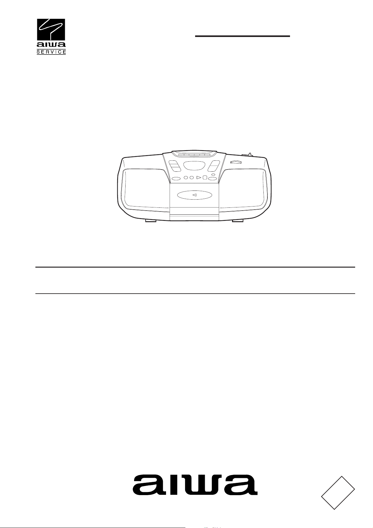
CSD-A240
LH
SERVICE MANUAL
COMPACT DISC STEREO
RADIO CASSETTE RECORDER
BASIC TAPE MECHANISM: ZZM-1 R5NC
BASIC CD MECHANISM: DA11T3C
S/M Code No. 09-013-442-8N1
DATA
Page 2

SPECIFICATIONS
<Tuner section>
Frequency range FM:
87.5 MHz to 108.0 MHz
Antenna: Rod antenna
AM:
530 kHz to 1,710 kHz
Antenna: Ferrite bar antenna
<Deck section>
Track format 4 tracks, 2 channels
Frequency range Normal tape: 50 - 12,500 Hz (EIAJ)
Recording system AC bias
Erasing system Magnet erase
Heads Recording/playback head (1),
Erasure head (1)
<CD player section>
Disc Compact disc
Scanning method Non-contact optical scanner
(semiconductor laser)
<General>
Speaker 100 mm cone type (2)
Output Headphones jack (stereo mini-jack)
Power output 2.5 W + 2.5 W
(EIAJ 7 ohms, T.H.D. 10 % DC),
1.9 W + 1.9 W
(DIN 1% Rated Power)
Power requirements DC 12 V using eight size C (R14)
batteries,
AC 110 - 120 V / 220 - 240 V
switchable, 50/60 Hz
Power consumption 17 W
Dimensions (W x H x D) 414 x 183 x 235 mm
Weight 3.2 kg (excluding batteries)
• Design and specifications are subject to change without
notice.
ACCESSORIES / PACKAGE LIST
PART NO.
1 8B-CDA-902-010 IB,LH(ESP)FM
!
2 87-A80-036-010 AC CORD SET ASSY,E W/FLTR V
!
3 87-A91-017-010 PLUG,CONVERSION JT-0476
NO.
DESCRIPTIONREF. NO. KANRI
– 2 –
Page 3
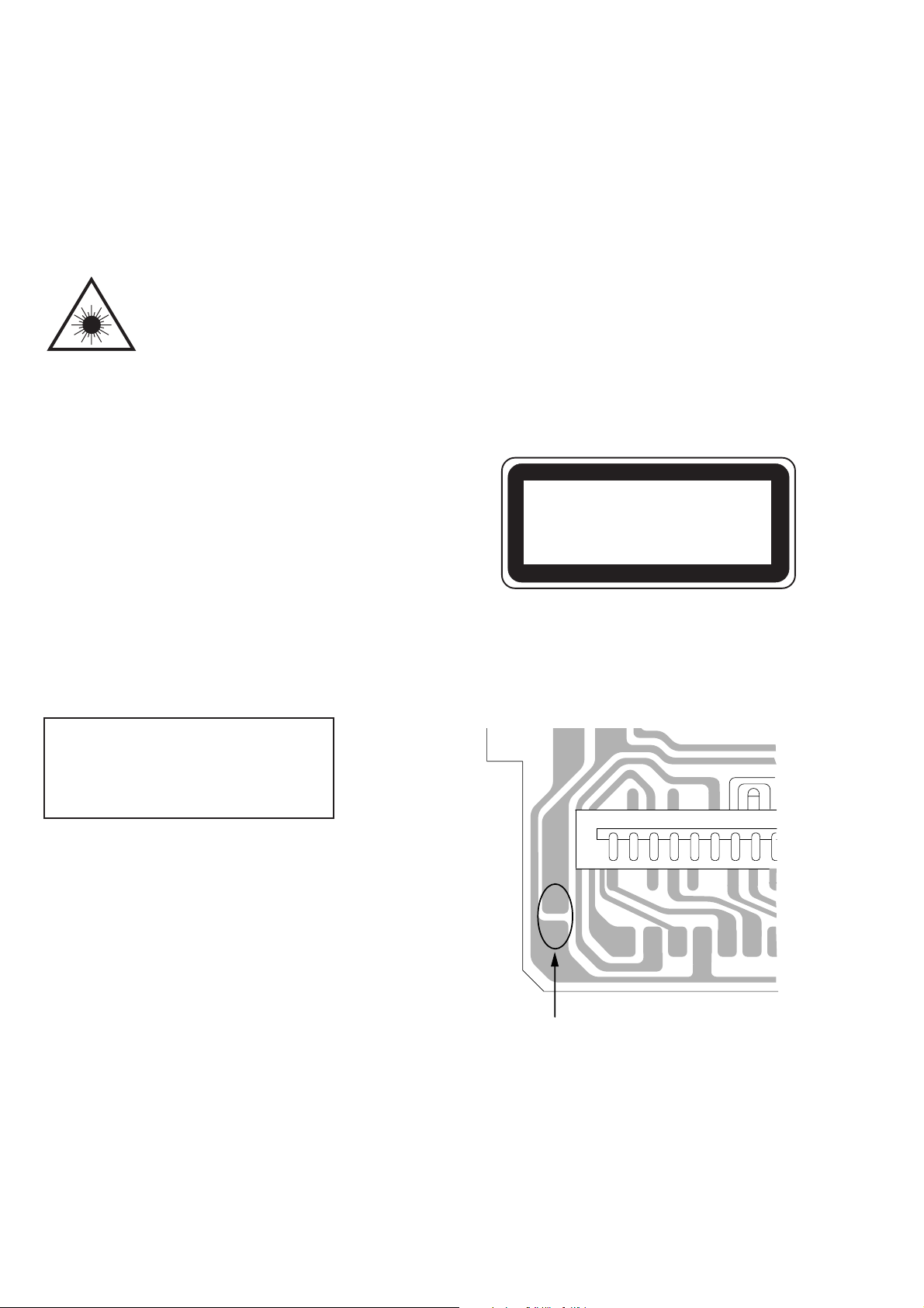
PROTECTION OF EYES FROM LASER BEAM DURING SERVICING
This set employs laser. Therefore, be sure to follow carefully
the instructions below when servicing.
WARNING!!
WHEN SERVICING, DO NOT APPROACH THE LASER
EXIT WITH THE EYE TOO CLOSELY. IN CASE IT IS
NECESSARY TO CONFIRM LASER BEAM EMISSION.
BE SURE TO OBSERVE FROM A DISTANCE OF MORE
THAN 30cm FROM THE SURFACE OF THE OBJECTIVE LENS ON THE OPTICAL PICK-UP BLOCK.
s Caution: Invisible laser radiation when
open and interlocks defeated avoid
exposure to beam.
s Advarsel: Usynlig laserståling ved åbning,
når sikkerhedsafbrydere er ude af funktion.
Undgå udsættelse for stråling.
VAROITUS!
Laiteen Käyttäminen muulla kuin tässä käyttöohjeessa
mainitulla tavalla saataa altistaa käyt-täjän
turvallisuusluokan 1 ylittävälle näkymättömälle
lasersäteilylle.
VARNING!
Om apparaten används på annat sätt än vad som
specificeras i denna bruksanvising, kan användaren
utsättas för osynling laserstrålning, som överskrider
gränsen för laserklass 1.
CAUTION
Use of controls or adjustments or performance of procedures other than those specified herin may result in
hazardous radiation exposure.
ATTENTION
L’utillisation de commandes, réglages ou procédures
autres que ceux spécifiés peut entraîner une dangereuse
exposition aux radiations.
ADVARSEL
Usynlig laserståling ved åbning, når sikkerhedsafbrydereer
ude af funktion. Undgå udsættelse for stråling.
This Compact Disc player is classified as a CLASS 1
LASER product.
The CLASS 1 LASER PRODUCT label is located on the
rear exterior.
CLASS 1 LASER PRODUCT
KLASSE 1 LASER PRODUKT
LUOKAN 1 LASER LAITE
KLASS 1 LASER APPARAT
Precaution to replace Optical block
(SF-P101NR)
Body or clothes electrostatic potential could
ruin laser diode in the optical block. Be sure
ground body and workbench, and use care the
clothes do not touch the diode.
1) After the connection, remove solder shown in
right figure.
PICK-UP Assy PWB
Solder
– 3 –
Page 4

ELECTRICAL MAIN PARTS LIST
REF. NO. DESCRIPTIONPART NO. KANRI
IC
87-A20-955-010 IC,LA1828
87-A21-193-010 IC,TA8227P
87-A21-443-040 C-IC,M62495AFP
87-A20-446-010 C-IC,LA9241ML
87-A21-319-010 C-IC,LC78622NE
87-A21-891-010 C-IC,MM1469XH
8B-CDL-600-010 C-IC,LC865516A-5T66
87-A21-607-010 IC,NJM14558LD
TRANSISTOR
89-327-143-080 C-TR,2SC2714O
87-026-447-080 TR,2SC1740SR
87-026-463-080 TR,2SA933SRS
87-A30-288-040 C-TR,DTC114YKA
89-318-154-080 TR,2SC1815Y
89-112-965-080 TR,2SA1296GR
87-026-291-080 TR,DTC124XS
87-A30-476-010 TR,KTA1046Y
87-026-462-080 TR,2SC1740SRS
89-109-332-380 TR,2SA933RS
87-A30-515-080 TR,2SA1979O/Y
87-A30-287-040 C-TR,DTC114TKA
87-A30-076-080 C-TR,2SC3052F
87-A30-431-040 C-TR,DTC124TKA
87-026-464-080 TR,DTC114TS
DIODE
87-A40-650-080 ZENER,MTZJ6.8A
87-070-345-080 DIODE,IN4148
87-A40-648-080 ZENER,MTZJ8.2A
87-A40-234-080 ZENER,MTZJ5.6A
87-017-978-080 DIODE,1N4003
87-017-932-080 ZENER,MTZJ6.2B
87-020-465-080 DIODE,1SS133
87-A40-465-010 DIODE,FR202
MAIN C.B
C211 87-A11-177-080 C-CAP,S 0.15-16 K B
C212 87-A11-177-080 C-CAP,S 0.15-16 K B
C215 87-016-460-080 C-CAP,S 0.22-16 B
C216 87-016-460-080 C-CAP,S 0.22-16 B
C231 87-010-213-080 C-CAP,S 0.015-50 B
C232 87-010-213-080 C-CAP,S 0.015-50 B
C233 87-A10-201-080 C-CAP,S0.33-16 KB
C234 87-A10-201-080 C-CAP,S0.33-16 KB
C235 87-016-669-080 C-CAP,S 0.1-25 K B
C236 87-016-669-080 C-CAP,S 0.1-25 K B
C237 87-010-371-080 CAP, ELECT 470-6.3V
C239 87-010-805-080 C-CAP,S 1-16 ZF
C240 87-010-805-080 C-CAP,S 1-16 ZF
C247 87-010-401-080 CAP, ELECT 1-50V
C248 87-010-401-080 CAP, ELECT 1-50V
C310 87-010-248-080 CAP, ELECT 220-10V
C316 87-010-263-080 CAP, ELECT 100-10V
C317 87-015-819-080 CAPACITOR,0.01
C801 87-010-248-080 CAP, ELECT 220-10V
C805 87-012-365-080 C-CAP,S 0.027-25VBK
C806 87-012-365-080 C-CAP,S 0.027-25VBK
C807 87-010-406-080 CAP, ELECT 22-50V
C808 87-010-406-080 CAP, ELECT 22-50V
C809 87-010-401-080 CAP, ELECT 1-50V
C810 87-010-401-080 CAP, ELECT 1-50V
C811 87-010-178-080 CHIP CAP 1000P
C812 87-010-178-080 CHIP CAP 1000P
C816 87-010-180-080 C-CER 1500P
C817 87-010-180-080 C-CER 1500P
KANRI
NO.
REF. NO. DESCRIPTIONPART NO.
C821 87-010-401-080 CAP, ELECT 1-50V
C822 87-010-401-080 CAP, ELECT 1-50V
C823 87-010-178-080 CHIP CAP 1000P
C824 87-010-178-080 CHIP CAP 1000P
C829 87-010-178-080 CHIP CAP 1000P
C830 87-010-178-080 CHIP CAP 1000P
C834 87-010-248-080 CAP, ELECT 220-10V
C843 87-A11-132-080 CAP, TC U 0.01-50 KB
C844 87-018-124-080 CAP, CER 270P-50V
C845 87-010-178-080 CHIP CAP 1000P
C846 87-010-263-080 CAP, ELECT 100-10V
C851 87-A11-128-080 CAP,TC U 4700P-50
C852 87-018-131-080 CAP, TC U 1000P
C853 87-A11-132-080 CAP,TC U 0.01-50 K B
CN201 87-099-018-010 CONN,16P
CN801 87-A60-110-010 CONN,4P V S2M-4W
CNA302 8B-CDA-629-010 CONN ASSY,6P MA-TU
CNA801 8B-CDA-630-010 CONN ASSY,4P RPH
JW108 87-003-097-080 COIL,1.0UH K LAL02
JW132 87-003-097-080 COIL,1.0UH K LAL02
JW133 87-003-097-080 COIL,1.0UH K LAL02
L801 87-007-342-010 COIL,OSC 85K BIAS
SW801 8Z-CD9-609-010 SW,SL 1-6-2 PS62D01
FRONT C.B
C601 87-018-150-080 CAP,TC-U 18P-50 CH
C602 87-018-111-080 CAP, CERA-SOL SS 27P
C603 87-018-116-080 CAP, CER 56P-50V
C604 87-018-149-080 CAP,TC-U 15P-50 CH
C605 87-018-114-080 CAP, CERA-SOL SS 39P
C606 87-010-197-010 CAP, S 0.01-25
C609 87-010-197-010 CAP, S 0.01-25
C610 87-A10-189-040 CAP,E 220-10
C611 87-010-196-010 C-CAP,S 0.1-25 F
C613 87-010-196-010 C-CAP,S 0.1-25 F
C614 87-010-264-040 CAP,E 100-10 5L
C615 87-010-197-010 CAP, S 0.01-25
C617 87-010-494-080 CAP ELECT GAS 1/50
C619 87-010-197-010 CAP, S 0.01-25
C621 87-010-494-080 CAP ELECT GAS 1/50
C622 87-010-493-080 CAP,E 0.47-50 GAS
C630 87-010-178-080 CAP, S 1000P-50
C631 87-010-178-080 CAP, S 1000P-50
C632 87-010-166-080 CAP, S 100P-50
C633 87-010-166-080 CAP, S 100P-50
CN601 87-099-033-010 16P 6216 H
CN602 87-099-201-010 CONN,8P 6216 H
FFC601 8B-CDA-620-010 FF-CABLE,16P FR-MAIN
L602 87-003-097-080 COIL,1.0UH K LAL02
L604 87-003-246-080 C-COIL,2125 33UH K
L608 87-003-231-080 C-COIL,2125 1UH K MLF2012
LED601 8A-CDA-645-010 LED,6224-10ID RED
LED602 8A-CDA-645-010 LED,6224-10ID RED
LED603 8A-CDA-645-010 LED,6224-10ID RED
LED604 8A-CDA-646-010 LED,6224-10GD GRN
LED606 8A-CDA-645-010 LED,6224-10ID RED
LED611 87-A41-066-010 LED,FR-12037G RED
S601 87-A91-704-080 SW,TACT EVQ 214 05R
S602 87-A91-704-080 SW,TACT EVQ 214 05R
S603 87-A91-704-080 SW,TACT EVQ 214 05R
S604 87-A91-704-080 SW,TACT EVQ 214 05R
S605 87-A91-704-080 SW,TACT EVQ 214 05R
S606 87-A91-704-080 SW,TACT EVQ 214 05R
S607 87-A91-704-080 SW,TACT EVQ 214 05R
S608 87-A91-704-080 SW,TACT EVQ 214 05R
S609 87-A91-704-080 SW,TACT EVQ 214 05R
S610 87-A91-704-080 SW,TACT EVQ 214 05R
S611 87-A91-704-080 SW,TACT EVQ 214 05R
S612 87-A91-704-080 SW,TACT EVQ 214 05R
NO.
– 4 –
Page 5

REF. NO. DESCRIPTIONPART NO.
NO.
X601 87-030-273-010 VIB,XTAL 32.768K5PPM
X602 87-030-376-080 VIB,CER CSA5.76MG200
CD C.B
C30 87-010-260-080 CAP, ELECT 47-25V
C251 87-010-405-080 CAP, ELECT 10-50V
C263 87-010-178-080 CHIP CAP 1000P
C264 87-010-178-080 CHIP CAP 1000P
C265 87-010-263-080 CAP, ELECT 100-10V
C266 87-010-263-080 CAP, ELECT 100-10V
C267 87-010-385-080 CAP, ELECT 220-25V
C268 87-010-385-080 CAP, ELECT 220-25V
C271 87-010-221-080 CAP, ELECT 470-10V
C272 87-010-221-080 CAP, ELECT 470-10V
C278 87-010-385-080 CAP, ELECT 220-25V
C279 87-010-235-080 CAP, ELECT 470-16V
C301 87-016-495-000 CAP,E 3300-25 M SMG
C306 87-010-404-080 CAP, ELECT 4.7-50V
C307 87-010-401-080 CAP, ELECT 1-50V
C308 87-010-221-080 CAP, ELECT 470-10V
C311 87-010-404-080 CAP,ELECT 4.7-50V
C312 87-010-385-080 CAP, ELECT 220-25V
C321 87-010-197-080 CAP, CHIP 0.01 DM
C322 87-010-263-080 CAP, ELECT 100-10V
C324 87-010-260-080 CAP, ELECT 47-25V
C325 87-010-405-080 CAP, ELECT 10-50V
C401 87-010-403-080 CAP, ELECT 3.3-50V
C402 87-010-197-080 CAP, CHIP 0.01 DM
C403 87-010-263-080 CAP, ELECT 100-10V
C404 87-010-248-080 CAP, ELECT 220-10V
C405 87-010-197-080 CAP, CHIP 0.01 DM
C406 87-010-374-080 CAP, ELECT 47-10V
C407 87-018-131-080 CAP,TC U 1000P-50
C408 87-010-198-080 CAP, CHIP 0.022
C409 87-010-248-080 CAP, ELECT 220-10V
C410 87-010-263-080 CAP, ELECT 100-10V
C411 87-A11-177-080 C-CAP,S 0.15-16 K B
C412 87-010-401-080 CAP, ELECT 1-50V
C413 87-016-369-080 C-CAP,S 0.033-25 B K
C414 87-010-405-080 CAP, ELECT 10-50V
C416 87-010-545-080 CAP, ELECT 0.22-50V
C417 87-012-157-080 C-CAP,S 330P-50 CH
C418 87-010-213-080 C-CAP,S 0.015-50 B
C419 87-A11-608-080 C-CAP,S 0.33-25 K B
C420 87-016-369-080 C-CAP,S 0.033-25 B K
C421 87-A11-177-080 C-CAP,S 0.15-16 K B
C422 87-010-184-080 CHIP CAPACITOR 3300P(K)
C423 87-010-992-080 C-CAP,S 0.047-25 B
C424 87-016-460-080 C-CAP,S 0.22-16 K B
C425 87-018-129-080 CAP,TC U 680P-50 K B
C426 87-A11-608-080 C-CAP,S 0.33-25 K B
C428 87-010-197-080 CAP, CHIP 0.01 DM
C429 87-010-186-080 CAP,CHIP 4700P
C430 87-012-156-080 C-CAP,S 220P-50 CH
C431 87-010-545-080 CAP, ELECT 0.22-50V
C432 87-010-374-080 CAP, ELECT 47-10V
C433 87-010-401-080 CAP, ELECT 1-50V
C434 87-010-184-080 CHIP CAPACITOR 3300P(K)
C435 87-010-197-080 CAP, CHIP 0.01 DM
C436 87-010-374-080 CAP, ELECT 47-10V
C437 87-010-404-080 CAP, ELECT 4.7-50V
C438 87-016-669-080 C-CAP,S 0.1-25 K B
C439 87-010-178-080 CHIP CAP 1000P
C440 87-018-139-080 CAP,TC U 1P-50 CH
C441 87-010-197-080 CAP, CHIP 0.01 DM
C442 87-018-109-080 CAP, TC U 22P-50 SL
C445 87-012-368-080 C-CAP,S 0.1-50 F
C446 87-012-368-080 C-CAP,S 0.1-50 F
C447 87-012-368-080 C-CAP,S 0.1-50 F
REF. NO. DESCRIPTIONPART NO.KANRI
C448 87-010-315-080 C-CAP,S 27P-50 CH
C451 87-012-156-080 C-CAP,S 220P-50 CH
C455 87-010-247-080 CAP, ELECT 100-50V
C457 87-010-312-080 C-CAP,S 15P-50 CH
C458 87-010-312-080 C-CAP,S 15P-50 CH
C459 87-010-263-080 CAP, ELECT 100-10V
C460 87-015-819-080 CAPACITOR,0.01
C461 87-010-197-080 CAP, CHIP 0.01 DM
C462 87-010-248-080 CAP, ELECT 220-10V
C463 87-A11-132-080 CAP, TC U 0.01-50 KB
C465 87-010-404-080 CAP, ELECT 4.7-50V
C466 87-012-368-080 C-CAP,S 0.1-50 F
C467 87-010-263-080 CAP, ELECT 100-10V
C469 87-012-154-080 C-CAP,S 150P-50 CH
C470 87-018-209-080 CAP, TC U 0.1-50 ZF
C471 87-018-209-080 CAP, TC U 0.1-50 ZF
C472 87-015-785-080 CHIP CAPACITOR, 0.1FZ-25Z
C473 87-015-785-080 CHIP CAPACITOR, 0.1FZ-25Z
C474 87-015-785-080 CHIP CAPACITOR, 0.1FZ-25Z
C475 87-A11-132-080 CAP, TC U 0.01-50 K B
C476 87-010-236-080 CAP,E 1000-10 SME
C477 87-010-197-080 CAP, CHIP 0.01 DM
C478 87-010-263-080 CAP, ELECT 100-10V
C479 87-010-197-080 CAP, CHIP 0.01 DM
C480 87-010-221-080 CAP, ELECT 470-10V
C481 87-010-405-080 CAP, ELECT 10-50V
C482 87-010-405-080 CAP, ELECT 10-50V
C489 87-012-368-080 C-CAP,S 0.1-50 F
C490 87-012-368-080 C-CAP,S 0.1-50 F
C491 87-A11-132-080 CAP, TC U 0.01-50KB
C492 87-010-221-080 CAP, ELECT 470-10V
C493 87-010-180-080 C-CER 1500P
C501 87-012-368-080 C-CAP,S 0.1-50 F
C502 87-010-322-080 C-CAP,S 100P-50 CH
C503 87-018-119-080 CAP,TC U 100P-50 KB
C504 87-010-322-080 C-CAP,S 100P-50 CH
C505 87-010-322-080 C-CAP,S 100P-50 CH
C506 87-010-322-080 C-CAP,S 100P-50 CH
C510 87-016-669-080 C-CAP,S 0.1-25 K B
C831 87-010-198-080 CAP, CHIP 0.022
CN202 8A-CH4-687-010 CONN,4P V 2.5
CN205 87-A60-109-010 CONN,2P V S2M-2W
CN301 8A-CH4-689-010 CONN,3P V 2.5
CN401 87-A60-424-010 CONN,16P V TOC-B
CN403 87-099-201-010 CONN,8P 6216 H
CN802 8A-CH4-687-010 CONN,4P V 2.5
CNA202 8B-CDA-633-010 CONN ASSY,4P SP
CNA205 8B-CDA-626-010 CONN ASSY,2P DOOR
CNA402 8B-CDA-625-010 CONN ASSY,6P CD-ME
CNA802 8B-CDA-631-010 CONN ASSY,4P TA-ME
FFC401 8B-CDA-621-010 FF-CABLE,16P CD-RF
FFC403 8B-CDA-622-010 FF-CABLE,8P CD-FR
J201 87-A60-420-010 JACK,3.5 ST (MSC)
L401 87-003-102-080 COIL, 10UH
L404 87-003-152-080 COIL, 100UH
R840 87-029-124-010 RES,FUSE 2.2-1/4
SFR430 87-024-437-080 SFR,100K RH063MC
X401 8Z-CD5-633-010 VIB, CER16.93MHZ FCR16.93M2
TUNER C.B
C1 87-010-314-080 C-CAP,S 22P-50V
C2 87-010-316-080 C-CAP,S 33P-50 CH
C3 87-010-314-080 C-CAP,S 22P-50V
C4 87-010-148-080 CAP, CHIP S 4P-50 CH
C5 87-010-378-080 CAP, ELECT 10-16V
C7 87-012-156-080 C-CAP,S 220P-50 CH
C8 87-010-197-080 CAP, CHIP 0.01 DM
C9 87-010-311-080 CAP 12P
C10 87-010-197-080 CAP, CHIP 0.01 DM
KANRI
NO.
– 5 –
Page 6
REF. NO. DESCRIPTIONPART NO. KANRI
C11 87-010-331-080 C-CAP,S 8P-50 UJ
C12 87-010-314-080 C-CAP,S 22P-50V
C13 87-010-322-080 C-CAP,S 100P-50 CH
C14 87-010-148-080 CAP, CHIP S 4P-50 CH
C15 87-016-669-080 C-CAP,S 0.1-25 K B
C16 87-010-178-080 CHIP CAP 1000P
C17 87-016-669-080 C-CAP,S 0.1-25 K B
C18 87-010-198-080 CAP, CHIP 0.022
C19 87-016-669-080 C-CAP,S 0.1-25 K B
C20 87-010-400-080 CAP, ELECT 0.47-50V
C21 87-010-403-080 CAP, ELECT 3.3-50V
C22 87-010-197-080 CAP, CHIP 0.01 DM
C24 87-010-197-080 CAP, CHIP 0.01 DM
C25 87-010-197-080 CAP, CHIP 0.01 DM
C26 87-012-358-080 C-CAP,S 0.47-10 F Z
C27 87-012-358-080 C-CAP,S 0.47-10 F Z
C28 87-010-992-080 C-CAP,S 0.047-25 B
C29 87-010-992-080 C-CAP,S 0.047-25 B
C30 87-010-248-080 CAP, ELECT 220-10V
C31 87-010-379-080 CAP, ELECT 22-16V
C32 87-010-197-080 CAP, CHIP 0.01 DM
C33 87-010-197-080 CAP, CHIP 0.01 DM
C34 87-010-197-080 CAP, CHIP 0.01 DM
C35 87-010-197-080 CAP, CHIP 0.01 DM
C36 87-010-263-080 CAP, ELECT 100-10V
C37 87-010-197-080 CAP, CHIP 0.01 DM
C38 87-010-197-080 CAP, CHIP 0.01 DM
C51 87-010-197-080 CAP, CHIP 0.01 DM
C56 87-010-327-080 C-CAP,S 4P-50 UJ
CF1 87-A90-128-010 FLTR,AM IF CFAL-455
CF2 87-008-261-010 FILTER, SFE10.7MA5-A
CF3 87-008-261-010 FILTER, SFE10.7MA5-A
CN2 87-A60-116-010 CONN,6P H S2M-6WR
D13 87-A40-916-040 C-VARI-CAP,HVC202A
L2 87-A50-560-010 COIL,FM BPF(ACD)
L3 8A-CD9-660-010 BAR-ANT,MW 2B-ACD(COI)
L4 87-A50-562-010 COIL,FM RF EX(ACD)
L5 87-A50-564-010 COIL,FM OSC EX(ACD)
L6 87-A50-337-010 COIL,AM OSC (TOKO)
L7 87-A50-579-010 COIL,AM IFT(ACD)
KANRI
NO.
REF. NO. DESCRIPTIONPART NO.
L8 87-A50-335-010 COIL,FM IFT (TOKO)
L9 87-A50-577-010 COIL,FM DET(ACD)
L10 87-005-849-080 COIL,10UH(CECS)
PVC1 87-A91-167-010 TUN-CAP,20P-160P FA-22125 N000
S1 87-A91-548-010 SW,SL-2-3 SK23E01G06
POWER C.B
C901 87-010-192-080 C-CAP,S 0.022-50 F
C902 87-010-192-080 C-CAP,S 0.022-50 F
C903 87-010-192-080 C-CAP,S 0.022-50 F
C904 87-010-192-080 C-CAP,S 0.022-50 F
CNA901 8B-CDA-627-010 CONN ASSY,3P PWR
!
J901 87-A60-178-010 JACK,AC E W/SW
!
PR901 87-A91-940-080 PROTECTOR,2.5A 20P 60V
!
PT901 8A-CDA-613-010 PT,H 2.5W
SP901 8A-CDA-214-010 SPR-C,BATT
SP902 8A-CDA-214-010 SPR-C,BATT
BATT C.B
SP903 8A-CDA-214-010 SPR-C,BATT
SP904 8A-CDA-214-010 SPR-C,BATT
VOLTAGE SEL C.B
!
SW901 87-A91-369-010 SW,AC SL 2-2-2 SDKGA41700
CD MOTOR C.B
M2 S0-M10-A09-700 MOTOR SLED ASSY
PN402 S2-369-750-000 PLUG,6P
SW1 S4-S13-A01-600 SW,LEAF
NO.
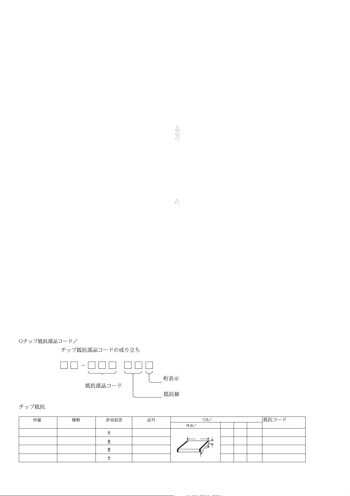
CHIP RESISTOR PART CODE
Chip Resistor Part Coding
88
A
Resistor Code
Chip resistor
Wattage Type Tolerance
1/16W 1005 5% CJ
1/16W
1/10W
1/8W
1608
2125
3216
5%
5%
5%
Symbol
CJ
CJ
CJ
Figure
Value of resistor
Form
L
– 6 –
Dimensions (mm)
t
W
0.55
Resistor Code
108
118
128
LW t
1.0 0.5 0.35 104
1.6 0.8 0.45
2 1.25 0.45
3.2
1.6
: A
: A
Page 7
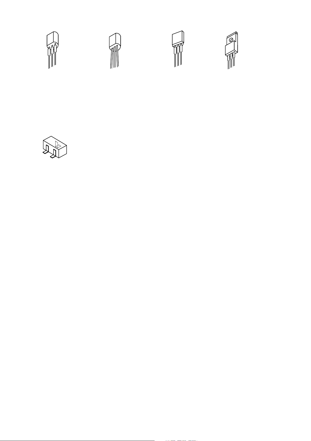
TRANSISTOR ILLUSTRATION
E C B
2SA1296GR
2SC1815Y
C
B
E
2SC2714O
2SC3052F
DTC114YKA
DTC114TKA
DTC124TKA
E C B
2SA1979O/Y
E C B
2SA933RS
2SA933SRS
2SC1740SR
2SC1740SRS
DTC124XS
DTC114TS
B C E
KTA1046Y
– 7 –
Page 8
WIRING 1 (MAIN 1 CD)
32 31 30 29 28 27 26 25 24 23 22 21 20 19 18 17 16 15 14 13 12 11 10 9 8 7 6 5 4 3 2 1
A
B
C
D
E
F
G
H
I
J
K
L
M
N
O
P
Q
8
R
S
T
U
Page 9
SCHEMATIC DIAGRAM – 1 (MAIN / CD : 1 / 2)
– 9 –
Page 10
SCHEMATIC DIAGRAM – 2 (CD : 2 / 2)
P101NR
PN402
– 10 –
Page 11
WIRING 2 (FRONT)
32 31 30 29 28 27 26 25 24 23 22 21 20 19 18 17 16 15 14 13 12 11 10 9 8 7 6 5 4 3 2 1
A
B
C
D
E
F
G
H
I
J
K
L
M
N
O
P
Q
11
R
S
T
U
Page 12
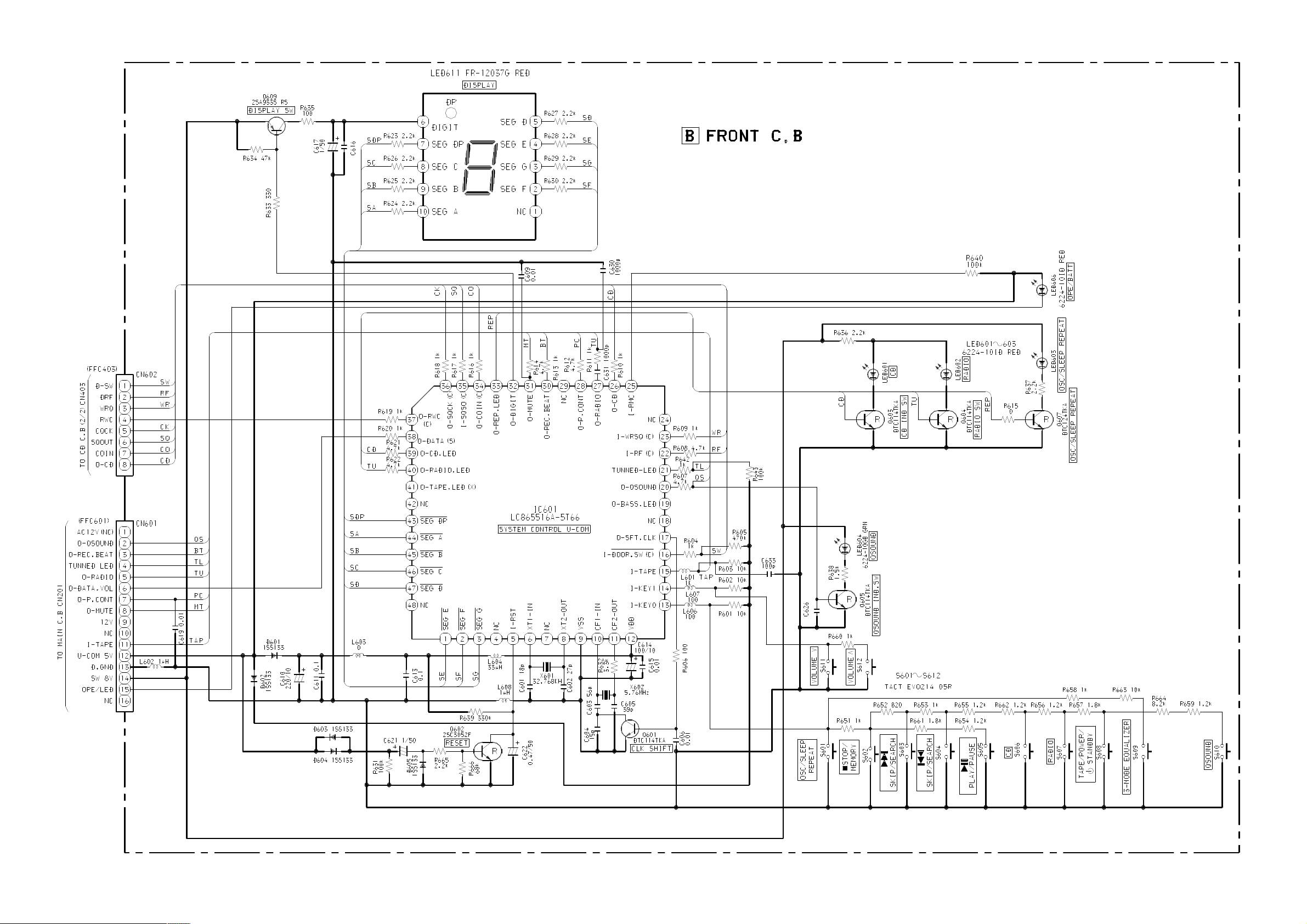
SCHEMATIC DIAGRAM – 3 (FRONT)
– 12 –
Page 13

WIRING 3 (TUNER)
151413121110987654321
A
B
C
D
E
F
G
H
I
J
K
L
M
N
O
P
Q
13
R
S
T
U
Page 14

SCHEMATIC DIAGRAM – 4 (TUNER)
– 14 –
Page 15

WIRING 4 (POWER / BATT / VOLTAGE SEL)
32 31 30 29 28 27 26 25 24 23 22 21 20 19 18 17 16 15 14 13 12 11 10 9 8 7 6 5 4 3 2 1
A
B
C
D
E
F
G
H
I
J
K
L
M
N
O
P
Q
15
R
S
T
U
Page 16

SCHEMATIC DIAGRAM – 5 (POWER / BATT / VOLTAGE SEL)
– 16 –
Page 17

WIRING – 5 (CD MOTOR)
H CD MOTOR C.B
M2
123456789101112131415
A
B
CNA402
TO CD C.B
+
_
6
5
3
PN402
1
M2
(SLED MOTOR)
SW1
(INSIDE LIMIT SW)
SW1
_
M1
M1
(SPINDLE MOTOR)
+
C
D
E
F
G
H
I
J
K
CD PICK UP ASSY
SF-P101NR
16
1
FFC401
L
M
N
O
P
Q
R
S
T
– 17 –
U
TO CD C.B
CN401
Page 18

IC BLOCK DIAGRAM
– 18 –
Page 19

EYE PATTERN
must be CLEAR and MAX
MAX
VOLT / DIV: 200mV
TIME / DIV: 0.5µs
0V
ADJUSTMENT <RADIO / TAPE / CD>
< RADIO SECTION >
1. AM Frequency Range Adjustment
• Test Point: TP5 (LCH), TP6 (RCH)
• Adjustment location:
L006 ....................................................................... 517kHz
TC003 ................................................................... 1750kHz
2. AM Tracking Adjustment
• Test Point: TP5 (LCH), TP6 (RCH)
• Adjustment location:
L003 ....................................................................... 600kHz
TC004 ................................................................... 1400kHz
3. AM IF Adjustment
• Test Point: TP5 (LCH), TP6 (RCH)
• Adjustment location:
L007 ....................................................................... 455kHz
4. FM Frequency Range Adjustment
• Test Point: TP5 (LCH), TP6 (RCH)
• Adjustment location:
L005 ........................................................................ 87MHz
TC001 .................................................................... 109MHz
5. FM Tracking Adjustment
• Test Point: TP5 (LCH), TP6 (RCH)
• Adjustment location:
L004 ........................................................................ 88MHz
TC002 .................................................................... 108MHz
< CD SECTION >
1. Focus Bias Adjustment
Make the focus bias adjustment when replacing and repairing
the optical block.
Oscilloscope
(DC range)
TP3 (RF)
TP4 (VREF)
1) Connect an oscilloscope to the test point TP3 (RF) and TP4
(VREF).
2) Turn on the power switch.
3) Insert test disc TCD-782 (YEDS-18) and play back the second
composition.
4) Adjust SFR430 so that the RF signal at the test point TP3 (RF)
is MAX and CLEAREST.
+
-
6. FM IF Adjustment
• Test Point: TP5 (LCH), TP6 (RCH)
• Adjustment location:
L008, L009 ...........................................................10.7MHz
< TAPE RECORDER SECTION >
1. Bias Adjustment
Settings: • Test tape: TTA-630
• Test point: TP2
• Adjustment location:
L801 ........................................... 85kHz±2kHz
2. Azimuth Adjustment
Settings: • Test tape: TTA-320
• Test point: PHONE JACK (J201)
• Adjustment location: Azimuth adjustment
screw
Method: Play back the test tape and adjust the screw so that the
output is maximum.
– 19 –
Page 20

IC DESCRIPTION
IC, LC78622NE
Pin No.
1 DEFI I Defect detection signal (DEF) input. ("L" is applied when not used.)
2 TAI I For PLL/Test input. (Connected to 0V)
3 PDO O Phase comparison output to control the external VCO.
4 VVSS – Ground of the built-in VCO. Normally 0V.
5 ISET I For the connection of a resistor which adjusts the PDO output current.
6 VVDD – Power supply of the built-in VCO.
7 FR I Adjusts the VCO frequency range.
8 VSS – Ground of digital circuits. Normally 0V.
9 EFMO O For slice level control/EFM signal output.
10 EFMIN I EFM signal input.
11 T2 I Test input. A pull-down resistor is incorporated. (Connected to 0V)
12 CLV+
13 CLV-
14 V/P O
15 HFL I Track detection signal input. Schmitt trigger input.
16 TES I Track error signal input. Schmitt trigger input.
17 TOFF O Tracking off output.
Pin Name I/O
O Disc motor control tri-state output.
Output to monitor the automatic switching between the rough servo control and phase servo
control. "H" : Rough servo, "L": Phase servo.
Description
18 TGL O Tracking gain switching output. "L" raises the gain.
19 JP+
20 JP-
21 PCK O
22 FSEQ O
23 VDD – Power supply of digital circuits.
24 SL+ O Controlled by serial data command issued by the microprocessor.
25 SL– O Controlled by serial data command issued by the microprocessor.
26 NC – Not connected.
27 PU IN I CD pickup inside limit switch.
28 RW O CD-RW disc select control.
29 EMPH O Deemphasis monitor. "H": when playing a deemphasis disc. (Not used)
30 C2F O C2 flag output. (Not used)
31 DOUT O Output a digital OUT signal. (EIAJ format) (Not used)
32 T3
33 T4
O Track jump control tri-state output.
Monitors the clock signal for EFM data playback. 4.3218MHz when the phase is locked.
(Not used)
Sync signal detection output. Goes "H" when the sync signal detected from the EFM
signal matches the sync signal generated internally. (Not used)
I Test input. (Connected to 0V)
34 NC – Not connected.
35 MUTEL O Lch 1-bit DAC/Lch muting output. (Not used)
36 LVDD – Lch power supply.
37 LCHO O Lch output.
38 LVSS – Lch ground. Normally 0V.
– 20 –
Page 21

Pin No.
39 RVSS – Rch 1-bit DAC/Rch ground. Normally 0V.
40 RCHO O Rch output.
41 RVDD – Rch power supply.
42 MUTER O Rch muting output. (Not used)
43 XVDD – Power supply of crystal oscillator.
44 XOUT O
45 XIN I
46 XVSS – Ground of crystal oscillator. Normally 0V.
47 SBSY O Subcode block sync signal output. (Not used)
48 EFLG O C1, C2, single, duplex correction monitor. (Not used)
49 PW O Output of subcodes P, Q, R, S, T, U and W. (Not used)
50 SFSY O Subcode frame sync signal output. Falls when the subcode is set to the standby state. (No used)
Pin Name
I/O Description
For the connection of a 16.93MHz crystal oscillator.
51 SBCK I
52 FSX O 7.35kHz sync signal output obtained by dividing the oscillator frequency. (Not used)
53 WRQ O Subcode Q standby output.
54 RWC I Read/write control input. Schmitt trigger input.
55 SQOUT O Subcode Q output.
56 COIN I Command input from the microprocessor.
57 CQCK I
58 RES I LC78622NE reset input.
59 T11 O Test output. Set to open (normally "L" output.) (Not used)
60 16M O 16.9344MHz output. (Not used)
61 4.2M O 4.236MHz output.
62 T5 I Test input. A pull-down resistor is incorporated. (Connected to 0V)
63 CS I Chip select input. (Connected to 0V)
64 T1 I Test input with no pull-down resistor. (Connected to 0V)
Subcode read-out clock input. Schmitt trigger input. ("L" is applied when not used.)
(Connected to 0V)
Command input retrieval clock or subcode retrieval clock input from SQOUT. Schmitt trigger
input.
– 21 –
Page 22

IC, LA9241ML
Pin No.
1 FIN2 I
2 FIN1 I For the connection of the pickup photodiode.
3EI
4 F I For the connection of the pickup photodiode.
5 TB I Inputs the DC components in the TE signal.
6 TE– I
7 TE O TE signal output.
8 TESI I TES (track error sense) comparator input. The TE signal is passed through a BPF.
9 SCI I Shock detection input.
10 TH I Sets the time constant for the tracking gain.
11 TA O TA amp output.
12 TD– I Composes the tracking phase compensation constant between the TD and VR pins.
13 TD O Sets the tracking phase compensation.
14 JP I Sets the amplitude of the tracking jump signal (kick pulses).
Pin Name I/O
For the connection of the pickup photodiode. Addition to the FIN1 pin creates an RF
signal and subtraction from it create an EF signal.
For the connection of the pickup photodiode. Subtraction from the F pin creates a TE
signal.
For the connection of a resistor which sets the gain of the TE signal between this pin
and the TE pin.
Description
15 TO O Tracking control signal output.
16 FD O Focusing control signal output.
17 FD– I Composes the focusing phase compensation constant between the FD and FA pins.
18 FA O Composes the focusing phase compensation constant between the FD- and FA- pins.
19 FA– I Composes the focusing phase compensation constant between the FA and FE pins.
20 FE O FE signal output.
21 FE– I
22 A-GND – Ground of analog signals.
23 SP O Single-ended output of the signals input to the CV+ and CV- pins.
24 SPI I Spindle amp input.
25 SPG I For the connection of a resistor which sets the gain in the spindle 12cm mode. (Not used)
26 SP– I For the connection of the spindle phase compensation constant with the SPD pin.
27 SPD O Spindle control signal output.
28 SLEQ I For the connection of sled phase compensation constant.
29 SLD O Sled control signal output.
30 SL–
31 SL+
For the connection of a resistor whichs sets the gain of the FE signal between this pin
and the TE pin.
I Sled feed signal input from the microprocessor.
32 JP–
33 JP+
34 TGL I Tracking gain control signal input from the DSP. Low gain when TGL is "H".
35 TOFF I Tracking off control signal input from the DSP. Off when TOFF is "H".
36 TES O Outputs the TES signal to the DSP.
I Tracking signal input from the DSP.
– 22 –
Page 23

Pin No.
37 HFL O
38 SLOF I Sled servo off control input.
I/O DescriptionPin Name
The HFL (high frequency level) signal is used to judge whether the main beam is positioned on
the pit or on the mirror.
39 CV–
40 CV+
41 RFSM O RF output.
42 RFS– O Sets the RF gain and the EFM signal's 3T compensation constant together with the RFSM pin.
43 SLC O
44 SLI I Input to control the DSP's data slice level.
45 D-GND – Ground of digital signals.
46 FSC O Output for the focus search smoothing capacitor.
47 TBC I The TBC (tracking balance control) signal sets the EF balance variation range.
48 NC – Not connected.
49 DEF O Disc defect detection output.
50 CLK I Reference clock input. 4.23MHz is input from the DSP.
51 CL I Microprocessor command clock input.
52 DAT I Microprocessor command data input.
53 CE I Microprocessor chip enable input.
54 DRF O DRF (detect RF) is an output to detect the RF level.
55 FSS I
I CLV error signal input from the DSP.
The SLC (slice level control) signal is output to control the DSP's data slice level of the RF
waveform.
The FSS (focus search select) signal switches the focus search modes (+/-search / +search with
respect to the reference voltage). (Not used)
56 VCC2 – VCC of servo and digital circuits.
57 REFI – For the connection of bypass capacitor for the reference voltage.
58 VR O Reference voltage output.
59 LF2 – Sets the time constant for disc defect detection.
60 PH1 – For the connection of a capacitor to hold the RF signal peak.
61 BH1 – For the connection of a capacitor to hold the RF signal bottom.
62 LDD O APC circuit output.
63 LDS I APC circuit input.
64 VCC1 – VCC of RF signal circuits.
– 23 –
Page 24

IC, LC865516A-5T66
Pin No. Pin Name I/O Description
1
SEG E
O
SEG E control.
10
11
12
13
14
15
16
17
18
2
3
4
5
6
7
8
9
SEG F
SEG G
NC
I-RST
XT1-IN
NC
XT2-OUT
VSS
CF1-IN
CF2-OUT
VDD
I-KEY0
I-KEY1
I-TAPE
I-DOOR SW (C)
O-SFT.CLK
NC
O
SEG F control.
O
SEG G control.
-
Not connected.
I
Microprocessor reset input.
I
Connected to an external 32.768 kHz crystal oscillator.
-
Not connected.
O
Connected to an external 32.768 kHz crystal oscillator.
-
GND.
I
Connected to an external 5.76 MHz ceramic filter.
O
Connected to an external 5.76 MHz ceramic filter.
-
Microprocessor power supply (+5 V).
I
Key AD input. (AD)
I
Key AD input. (AD)
I
Deck status input. (AD)
I
CD door switch status input.
O
Main clock shift output.
-
Not connected.
19
20
21
22
23
24
25
26
27
28
29
30
31
32
33
34
35
O-BASS.LED
O-QSOUND
TUNNED-LED
I-RF(C)
I-WRSQ(C)
NC
I-RMC
O-CD
O-RADIO
O-P.CONT
NC
O-REC.BEAT
O-MUTE
O-DIGIT
O-REP.LED
O-COIN(C)
I-SQSO(C)
O
BASS LED ON/OFF control output. (Not used)
O
QSOUND LED ON/OFF control output.
O
TUN LED ON/OFF control output.
I
CD RF level detection input.
I
CD subcode Q standby input.
-
Not connected.
I
Remote control input.
O
CD power control output.
O
RADIO power control output.
O
The main power supply control output.
-
Not connected.
O
Beat switch control output.
O
Main mute output.
O
7-segment LED power supply control output.
O
REPEAT LED ON/OFF control output.
O
CD command output.
I
CD subcode Q input.
36
37
38
39
40
41
O-SQCK(C)
O-RWC(C)
O-DATA(S)
O-CD.LED
O-RADIO.LED
O-TAPE.LED(X)
O
CD command/CLK for subcode.
O
CD read/write control output.
O
Data output to M62495AFP.
O
LED ON/OFF control output for the CD function.
O
LED ON/OFF control output for the RADIO function.
O
LED ON/OFF control output for the TAPE function. (Not used)
– 24 –
Page 25

Pin No. Pin Name I/O Description
42
NC
- Not connected.
43
44
45
46
47
48
SEG DP
SEG A
SEG B
SEG C
SEG D
NC
O SEG DP control.
O SEG A control.
O SEG B control.
O SEG C control.
O SEG D control.
- Not connected.
– 25 –
Page 26

VOLTAGE CHART
IC001, LA1828
IC401, LA9241ML
PIN NO. FM AM
1 0.93 0
200
3 4.73 4.88
4 4.73 4.88
5 4.68 4.88
600
7 1.24 1.24
8 1.35 1.36
900
10 4.22 0
11 0.01 3.2
12 4.8 4.88
13 0.59 0.3
14 1.27 1.25
15 1.27 1.25
16 0 0
17 0 0
18 4.8 4.88
19 0.01 0
20 4.8 4.88
21 4.8 4.88
PIN NO. ACTIVE STATIC
1 2.67 2.53
2 2.65 2.53
3 2.67 2.53
4 2.67 2.56
5 2.67 2.53
6 2.66 2.55
7,8 2.67 2.55
9 2.65 2.54
10 2.66 2.52
11 2.67 2.55
12 2.7 2.54
13 2.67 2.55
14 2.7 2.54
15 2.72 2.54
16 2.69 2.54
17 2.67 2.55
18 2.69 2.55
19 2.73 2.54
20 2.69 2.54
21 0 2.54
22 2.67 0
PIN NO. ACTIVE STATIC
45 0 0
46 2.64 2.54
47 2.65 2.55
48 0 0
49 0 0
50 2.54 2.44
51 4.77 4.71
52 4.86 4.71
53 0 0.07
54 5.11 0.03
55 0.16 0.14
56 5.2 5.01
57 2.64 2.54
58 2.64 2.56
59 2.59 0.98
60 2.57 0.99
61 2.3 2.24
62 3.86 4.35
63 0.19 0
64 5.18 5.02
22 4.8 4.88
23 0 0
24 0.33 1.26
IC202, TA8227P
PIN NO. ACTIVE STATIC
1 12.31 11.5
2 6.57 6.1
3 12 1.5
400
5 0.56 0.56
600
700
8 0.56 0.56
9 6.65 6.41
10 12 1.42
11 6.46 6.2
12 13.1 12.5
23 2.67 2.53
24 2.65 2.54
25 2.69 2.56
26 2.75 2.56
27 2.75 2.5
28 2.68 2.55
29 2.75 2.55
30 2.45 2.33
31 2.45 2.34
32,33 0 0
34 5.22 5.01
35 0 5.01
36 1.4 0.04
37 0 0.01
38 0 5
39 0 0
40 0.25 0
41 2.45 1.61
42 2.54 2.45
43 2.54 2.41
44 2.63 2.53
– 26 –
Page 27

IC402, LC78622NE
PIN NO. ACTIVE STATIC
100
200
3 1.8 0.01
400
5 2.1 1.85
6 5.6 4.98
7 0.4 0.07
800
9 2.8 2.52
10 2.7 2.41
11 0 0
12 0.3 0
13 0 0
14 0 5
15 0 0.01
16 1.5 0.04
17 0 5.01
18 5.6 5.01
19,20 0 0
21 2.7 2.48
22 5.6 0
23 5.6 5.02
24,25 0 0
26 0 5
27 5.6 5
28,29 0 0
30 0 4.95
31 2.8 2.48
32~34 0 0
35 0 5.02
36 5.3 4.77
37 2.15 1.94
38,39 0 5
40 2.15 1.95
41 5.3 4.77
42 0 5
43 5.5 5.02
44 2.3 2.08
45 2.3 2.06
46 2.3 0
47 0.1 0.08
PIN NO. ACTIVE STATIC
48 0 2.27
49 0.1 0
50 2.77 2.5
51 0 0
52 2.77 2.5
53 0.9 0
54 0 0.07
55 0 0
56 5.16 4.71
57 5 4.71
58 5.5 5
59 0 0
60 2.25 2.02
61 2.66 2.41
62~64 0 0
IC404, MM1469XH
PIN NO. ACTIVE STATIC
1 4.2 3.61
2 4.2 3.62
3,4 2.95 2.54
5 8.2 7.24
6,7 5.8 5.02
800
9 2.95 2.55
10 3 2.55
11 4.27 3.61
12 4.01 3.63
13 0 0
14 8.4 7.39
15 1.45 0.78
16 1.45 0.8
17 4.1 3.63
18 4.1 3.62
19 2.9 2.54
20 2.9 2.55
21,22 8.9 7.96
23,24 2.9 2.55
25 2.9 2.54
26 4.5 3.61
27 3.71 3.62
28 0 0
IC801, NJM14558LD
PIN NO. TAPE REC
1 3.37 3.38
2 3.37 3.39
3 3.34 3.35
400
5 3.34 3.35
6 3.37 3.39
7 3.37 3.38
8 6.83 6.82
– 27 –
Page 28

IC203, M62495AFP
PIN NO. CD TAPE TUNER
1 2.54 2.55 2.56
2 2.55 2.55 2.56
3 2.55 2.55 2.56
4 0.7 0.8 2.56
5 2.54 2.55 2.57
6 2.56 2.56 2.57
7 2.55 2.55 2.57
8 2.55 2.56 2.57
9 2.55 2.55 2.56
10 2.55 2.55 2.57
11 2.56 2.56 2.57
12 5.08 5.09 5.11
13 2.82 2.83 2.83
14 0 0 0
15 2.55 2.55 2.56
16 2.55 2.55 2.56
17 2.55 2.56 2.57
18 2.55 2.55 2.56
19 2.57 2.57 2.58
20 2.54 2.55 2.57
21 0.7 0.58 0.69
22 2.54 2.06 2.56
23 2.55 2.56 2.56
24 2.54 2.55 2.56
PIN NO. TAPE TUNER CD
16 0 0 4.84
17 0.03 0.02 0
18 1.2 0 0
19 4.8 4.9 4.76
20 0.03 0.03 0.01
21 5.23 5.34 5.2
22 0 0 0.01
23 0.04 0.05 0.01
24 0 0 0
25 4.77 4.86 4.74
26 0.06 0.05 4.75
27 0.06 4.9 0.04
28 4.76 4.87 4.71
29 0 0.06 0
30 0.06 0.06 0.04
31 0.06 0.06 0.04
32 0.26 0.16 0.24
33 0.07 0.06 0.04
34 0.05 0.05 4.75
35 0.08 0.09 1.94
36 0.05 0.05 4.75
37 0.05 0.05 0.03
38 0.06 0.06 0.04
39 0.05 0.05 4.72
40 0.05 4.86 0.03
IC601, LC865516A-5T66
PIN NO. TAPE TUNER CD
1 0.12 0.12 0.1
2 0.12 0.11 0.09
3 0.12 0.11 8.53
4 0.07 0.03 0.26
5 4.65 4.7 4.61
6 1.59 1.64 1.58
7 00 0
8 2.52 2.58 2.49
9 0 0.02 0
10 2.11 4.4 2.09
11 2.25 4.9 2.23
12 4.8 4.9 4.76
13 4.99 5.1 5.06
14 4.99 5.1 5.06
15 0.9 5.1 5.07
41 4.79 0.05 0.03
42 0.34 2.82 2.39
43 9.54 9.44 6.11
44 0.12 0.12 0.1
45 9.55 9.11 0.11
46 0.12 0.12 0.1
47 0.12 0.12 0.1
48 2.3 2.3 2.2
– 28 –
Page 29

Q001
Q302
Q401
PIN FM AM
E 2.22 2.21
C 4.07 4.06
B 2.95 2.95
Q002
PIN FM AM
E 4.82 4.9
C88
B 5.52 5.58
Q003
PIN FM AM
E 5.53 5.59
C 5.52 5.59
B 4.85 4.9
Q004
PIN ACTIVE STATIC
E 11.5 11.99
C 11.4 12
B 10.9 11.32
Q303
PIN ACTIVE STATIC
E00
C00
B 4.57 4.57
Q304
PIN ACTIVE STATIC
E 11.38 11.97
C 7.94 7.98
B 10.75 11.34
Q305
PIN ACTIVE STATIC
E 4.46 4.99
C 2.11 1.56
B 3.76 4.35
Q402
PIN ACTIVE STATIC
E 7.87 7.97
C 5.3 5.15
B 7.17 7.28
Q403
PIN ACTIVE STATIC
E 2.56 2.56
C 2.56 2.56
B00
Q406
PIN FM AM
E00
C 4.06 4.12
B 2.98 3.03
Q243
PIN ACTIVE STATIC
E00
C00
B 0.12 0.64
Q244
PIN ACTIVE STATIC
E00
C00
B 0.12 0.64
Q301
PIN ACTIVE STATIC
E 7.23 7.26
C 10.56 11.23
B 7.85 7.87
Q306
PIN ACTIVE STATIC
E 5.08 5.09
C 7.94 7.98
B 10.75 5.81
Q310
PIN ACTIVE STATIC
E 5.55 5.56
C 10.45 10.83
B 6.25 6.26
Q321
PIN ACTIVE STATIC
E00
C 4.6 4.6
B00
Q407
PIN ACTIVE STATIC
E 4.6 4.58
C 2.57 2.55
B 2.56 2.55
Q408
PIN ACTIVE STATIC
E 4.6 4.58
C 2.57 0.55
B 2.56 2.55
Q491
PIN ACTIVE STATIC
E 12.2 12.66
C 11.4 12
B 11.5 11.99
PIN ACTIVE STATIC
E00
C 0.01 0.02
B 0.6 0.7
– 29 –
PIN ACTIVE STATIC
E 7.91 7.98
C 7.88 7.97
B 7.15 7.23
Page 30

Q492
PIN ACTIVE STATIC
E00
C 0.14 0.14
B 4.41 4.41
Q801
PIN TAPE REC
E 0 1.64
C 0 5.9
B 0 2.31
Q810
PIN TAPE REC
E 3.36 3.38
C 0.05 13.85
B 0.13 0.13
Q841
PIN TAPE REC
E00
C 0.72 0.01
B 0 5.73
– 30 –
Page 31

MECHANICAL EXPLODED VIEW 1 / 1
39
49
ZZM-1
R5NC
11
12
33
28
13
14
15
16
17
18
19
A
F
A
47
A
A
A
5
7
20
8
A
21
29
30
31
32
34
36
52
B
37
B
9
6
PWB
48
C
35
37
C
PWB
58
41
G
E
38
53
A
54
40
42
43
A
A
D
J
A
45
H
D
46
51
D
G
44
PWB
55
56
PWB
PLATE,ANT
59
57
25
A
26
A
I
27
11
10
24
22
A
A
23
A
4
2
1
38
3
A
PWB
A
50
CSD-A240 LHWC,LHSC,LHDC,LHGC,LHPC,LHLC
(FileName:EXP.EPS)
13/2/8 BCD-A
– 31 –
Page 32

MECHANICAL PARTS LIST 1 / 1
PART NO. DESCRIPTIONREF. NO. KANRI
NO.
1 8B-CDA-009-010 WINDOW,CASS<[W],[S]>
1 8B-CDA-086-010 WINDOW,CASS (D)<[D]>
1 8B-CDA-093-010 WINDOW,CASS (G)<[G]>
1 8B-CDA-154-010 WINDOW,CASS (P)<[P]>
1 8B-CDA-073-010 WINDOW,CASS (L)<[L]>
2 8B-CDA-132-010 LID,CASS U (W)<[W]>
2 8B-CDA-003-010 LID,CASS<EXCEPT [W]>
3 8B-CDA-208-010 SPR-T,CASS
4 8B-CDA-089-010 WINDOW,DISP LH<[W],[S]>
4 8B-CDA-127-010 WINDOW,DISP LH (D)<[D]>
4 8B-CDA-125-010 WINDOW,DISP LH (G)<[G]>
4 8B-CDA-126-010 WINDOW,DISP LH (P)<[P]>
4 8B-CDA-124-010 WINDOW,DISP LH (L)<[L]>
5 8B-CDA-058-010 CABI ASSY,FRONT LH (W)<[W]>
5 8B-CDA-161-010 CABI ASSY,FRONT LH<[S]>
5 8B-CDA-056-010 CABI ASSY,FRONT LH (D)<[D]>
5 8B-CDA-066-010 CABI ASSY,FRONT LH (G)<[G]>
5 8B-CDA-067-010 CABI ASSY,FRONT LH (P)<[P]>
5 8B-CDA-059-010 CABI ASSY,FRONT LH (L)<[L]>
6 8B-CDA-087-010 WINDOW,TU LH<EXCEPT [L]>
6 8B-CDA-088-010 WINDOW,TU LH (L)<[L]>
7 8B-CDA-017-010 KEY,FUNC C
8 8B-CDA-014-010 KEY,CD
9 8B-CDA-016-010 KEY,FUNC B
10 8B-CDA-011-010 KNOB,RTRY TU
11 8B-CDA-615-010 SPKR,10 7OHM
12 8B-CDA-019-010 KEY,PAUSE<[W],[S]>
12 8B-CDA-149-010 KEY,PAUSE (D)<[D]>
12 8B-CDA-095-010 KEY,PAUSE (G)<[G]>
12 8B-CDA-160-010 KEY,PAUSE (P)<[P]>
12 8B-CDA-076-010 KEY,PAUSE (L)<[L]>
13 8B-CDA-020-010 KEY,STOP<[W],[S]>
13 8B-CDA-148-010 KEY,STOP (D)<[D]>
13 8B-CDA-096-010 KEY,STOP (G)<[G]>
13 8B-CDA-159-010 KEY,STOP (P)<[P]>
13 8B-CDA-077-010 KEY,STOP (L)<[L]>
14 8B-CDA-021-010 KEY,FF<[W],[S]>
14 8B-CDA-147-010 KEY,FF (D)<[D]>
14 8B-CDA-097-010 KEY,FF (G)<[G]>
14 8B-CDA-158-010 KEY,FF (P)<[P]>
14 8B-CDA-078-010 KEY,FF (L)<[L]>
15 8B-CDA-022-010 KEY,REW<[W],[S]>
15 8B-CDA-146-010 KEY,REW (D)<[D]>
15 8B-CDA-098-010 KEY,REW (G)<[G]>
15 8B-CDA-157-010 KEY,REW (P)<[P]>
15 8B-CDA-079-010 KEY,REW (L)<[L]>
16 8B-CDA-023-010 KEY,PLAY<[W],[S]>
16 8B-CDA-145-010 KEY,PLAY (D)<[D]>
16 8B-CDA-099-010 KEY,PLAY (G)<[G]>
16 8B-CDA-156-010 KEY,PLAY (P)<[P]>
16 8B-CDA-080-010 KEY,PLAY (L)<[L]>
17 8B-CDA-024-010 KEY,REC<[W],[S]>
17 8B-CDA-144-010 KEY,REC (D)<[D]>
17 8B-CDA-100-010 KEY,REC (G)<[G]>
17 8B-CDA-155-010 KEY,REC (P)<[P]>
17 8B-CDA-081-010 KEY,REC (L)<[L]>
18 8A-CDA-221-010 SPR-P,REC
19 8A-CDA-220-010 PLATE,REC
20 8B-CDA-008-010 PANEL,TOP<[W],[S]>
20 8B-CDA-085-010 PANEL,TOP (D)<[D]>
20 8B-CDA-106-010 PANEL,TOP G<[G]>
20 8B-CDA-133-010 PANEL,TOP (P)<[P]>
20 8B-CDA-136-010 PANEL,TOP U (L)<[L]>
21 8B-CDA-201-010 HLDR,LED
22 8B-CDA-040-010 POINTER,TU
DESCRIPTIONREF. NO. KANRI
PART NO.
23 8B-CDA-202-010 HLDR,TU
24 8A-CDA-216-110 GEAR,TU B
25 8A-CDA-203-110 GUIDE,GEAR
26 8A-CDA-202-110 GEAR,RELAY
27 8A-CDA-215-010 DRUM,TU
28 86-CT9-217-110 HLDR,CHUCK A(S)
29 86-CT9-222-010 PLATE,MAGNET
30 87-036-368-010 MAGNET
31 8Z-CT6-213-110 BASE,CHUCK
32 8Z-CT6-214-110 RING,CHUCK
33 8B-CDA-006-010 LID,CD<[W],[S]>
33 8B-CDA-084-010 LID,CD (D)<[D]>
33 8B-CDA-104-010 LID,CD G<[G]>
33 8B-CDA-129-010 LID,CD (P)<[P]>
33 8B-CDA-135-010 LID,CD U (L)<[L]>
34 8B-CDA-063-010 CHAS,CD (W)<[W]>
34 8B-CDA-005-010 CHAS,CD<EXCEPT [W]>
35 8B-CDA-206-010 SPR-T,CD
36 8Z-CDB-169-010 PANEL,CD SANYO
37 88-CH6-220-010 CUSHION,CD A
38 87-063-165-010 OIL-DMPR 150
39 8B-CHA-021-010 HANDL,ARM W<[W]>
39 8B-CDA-007-010 HANDL,ARM<EXCEPT [W]>
40 8B-CHA-022-010 LID,HANDL W<[W]>
40 8B-CDA-010-010 LID,HANDL<EXCEPT [W]>
!
41 8Z-CD5-634-010 COVER,AC SOCKET
!
42 87-A60-178-010 JACK,AC E W/SW
43 8A-CDA-613-010 PT,H 2.5W
!
44 8B-CDA-069-010 CABI,REAR LH (W)<[W]>
44 8B-CDA-030-010 CABI,REAR LH<EXCEPT [W]>
45 8B-CDA-018-010 KNOB,SL BAND
46 8B-CHA-020-010 LID,BATT W<[W]>
46 8B-CDA-004-010 LID,BATT<EXCEPT [W]>
47 87-064-185-010 HLDR,WIRE
48 87-036-389-010 SW,PUSH LOCK
49 87-A91-857-010 ANT,ROD 5SEC709
50 88-CD6-661-010 HLDR,BAR ANT.
!
51 87-A91-369-010 SW,AC SL 2 2 2 SDKGA41700
52 M8-ZZK-E90-070 DA11T3C
53 8B-CDA-621-010 FF-CABLE,16P CD-RF
54 8B-CDA-626-010 CONN ASSY,2P DOOR
55 8B-CDA-622-010 FF-CABLE,8P CD-FR
56 8B-CDA-633-010 CONN ASSY,4P SP
57 8B-CDA-630-010 CONN ASSY,4P RPH
58 8B-CDA-620-010 FF-CABLE,16P FR-MAIN
59 8B-CDA-631-010 CONN ASSY,4P TA-ME
A 87-751-096-410 VT2+3-10 GLD
B 87-721-096-410 QT2+3-10 GLD
C 8A-CK4-223-010 S-SCREW,CD
D 87-751-104-410 VT2+3-30
E 87-254-097-410 U+3-12 CR
F 8A-CDA-222-010 S-SCREW,CASS+2.6-4
G 87-751-076-410 SCREW 2.6-12
H 87-B10-183-010 VT2+3-20 W/O SOLT
I 87-261-073-410 V+2.6-6
J 87-721-074-410 QT2+2.6-8 W/O SLOT
NO.
– 32 –
Page 33

COLOR NAME TABLE
Basic color symbol Color Basic color symbol Color Basic color symbol Color
B Black C Cream D Orange
G Green H Gray L Blue
LT Transparent Blue N Gold P Pink
R Red S Silver ST Titan Silver
T Brown V Violet W White
WT Transparent White Y Yellow YT Transparent Yellow
LM Metallic Blue LL Light Blue GT Transparent Green
LD Dark Blue DT Transparent Orange GM Metallic Green
YM Metallic Yellow DM Metallic Orange PT Transparent Pink
LA Aqua Blue GL Light Green HT Transparent Gray
– 33 –
Page 34

TAPE MECHANISM EXPLODED VIEW 1 / 1
12
11
TERMINAL,LB1
A
2
10
9
4
3
1
8
14
7
55
42
6
5
13
53
B
19
17
16
21
20
22
27
24
23
15
18
28
26
25
C
54
29
31
30
48
50
51
52
49
47
46
45
44
43
41
36
40
37
32
39
33
34
1
35
38
– 34 –
Page 35

TAPE MECHANISM PARTS LIST 1 / 1
PART NO. DESCRIPTIONREF. NO. KANRI
NO.
1 8Z-ZM1-254-310 SPR-C,REEL R
2 8Z-ZM1-225-110 GEAR,REEL R
3 8Z-ZM1-253-210 SPR-C,AUTO SENSOR
4 8Z-ZM1-217-110 LEVER,AUTO SENSOR
5 8Z-ZM1-212-110 LEVER,T-UP
6 8Z-ZM1-245-310 SPR-T,AUTO
7 8Z-ZM1-236-010 CLR,SLIP FF/REW
8 8Z-ZM1-252-110 SPR-C,FF/REW
9 8Z-ZM1-230-010 GEAR,SLIP FF/REW A
10 8Z-ZM1-269-010 FELT,FF/REW 2
11 8Z-ZM1-238-110 GEAR,SLIP FF/REW B 2
12 8Z-ZM1-237-110 LEVER,FF/REW 2
13 8Z-ZM1-283-010 LEVER,PAUSE 2
14 8Z-ZM1-222-010 LEVER,E-LOCK M
15 8Z-ZM1-219-010 LEVER,E-OPEN
16 8Z-ZM1-244-110 SPR-T,T-UP
17 8Z-ZM1-247-310 SPR-T,PINCH
18 8Z-ZM1-261-110 ROLLER ASSY,PINCH
19 8Z-ZM1-221-210 LEVER,PINCH
20 8Z-ZM1-205-310 LEVER,PLAY
21 8Z-ZM1-248-210 SPR-T,BRG
22 87-A92-207-010 HEAD,AP-4211T4
23 84-ZM2-227-310 SPR-C,AZIMUTH
24 8Z-ZM1-216-110 LEVER,AUTO
25 8Z-ZM1-246-110 SPR-T,AUTO 2
26 8Z-ZM1-233-110 GEAR,IDL REW
27 8Z-ZM1-208-010 LEVER,STOP
28 8Z-ZM1-207-010 LEVER,FF
29 8Z-ZM1-206-010 LEVER,REW
30 8Z-ZM1-211-210 LEVER,REC 2
DESCRIPTIONREF. NO. KANRI
PART NO.
NO.
31 87-A91-819-010 HEAD,EH 2NSS-2200
32 8Z-ZM1-215-010 LEVER,REC LOCK
33 87-A91-492-010 SW,LEAF MSW18560
34 8Z-ZM1-226-010 GEAR,REEL L
35 8Z-ZM1-241-210 SPR-T,PLAY
36 8Z-ZM1-220-110 LEVER,REC SENSOR
37 8Z-ZM1-249-210 SPR-T,FR
38 8Z-ZM1-242-310 SPR-T,FF/REW
39 8Z-ZM3-244-010 GEAR,CAM TD20
40 8Z-ZM1-232-010 GEAR,IDL FF/REW
41 82-ZM1-290-010 FLY-WHL ASSY,ZZM1
42 8Z-ZM1-275-010 W-L,1.47-4-0.25
43 8Z-ZM1-228-010 GEAR,SLIP T-UP B
44 8Z-ZM1-265-010 FELT,T-UP
45 8Z-ZM1-227-010 GEAR,SLIP T-UP A
46 8Z-ZM1-251-210 SPR-C,T-UP SLIP
47 8Z-ZM1-243-310 SPR-T,STOP/PAUSE
48 87-A91-825-010 MOT,M09Y/Z
49 8Z-ZM1-271-010 PULLEY,MOT ZZM-1
50 8Z-ZM1-264-010 BELT,MAIN S
51 8Z-ZM1-260-010 SPR-P,CASETTE
52 8Z-ZM1-201-910 CHAS ASSY,ZZM-1
53 8Z-ZM1-255-310 SPR-T,E-LOCK
54 8Z-ZM1-214-210 LEVER,LOCK
55 8Z-ZM1-257-110 SPR-C,F/R
A 84-ZM2-242-010 S-SCREW,AZ1-2-6.4
B 8Z-ZM1-270-110 V+2.6 ZZM-1
C 87-B10-301-010 W-L,1.63-3.2-0.5 SLIT
– 35 –
Page 36

CD MECHANISM EXPLODED VIEW 1 / 1
1
SW1
M1
A
2
3
4
CD MOTOR C.B
CD MECHANISM PARTS LIST 1 / 1
PART NO.
1 M8-ZZK-E90-070 DA11T3C
2 S2-121-A28-400 COVER GEAR
3 S2-511-A21-000 GEAR MIDDLE
4 S2-511-A21-100 GEAR,DRIVE
A S1-PN2-03R-OSE SCR PAN PCS 2-3
NO.
DESCRIPTIONREF. NO. KANRI
M2
PN402
– 36 –
Page 37

2–11, IKENOHATA 1–CHOME, TAITO-KU, TOKYO 110, JAPAN TEL:03 (3827) 3111
Printed in Singapore9301978 2000041 0251431
 Loading...