

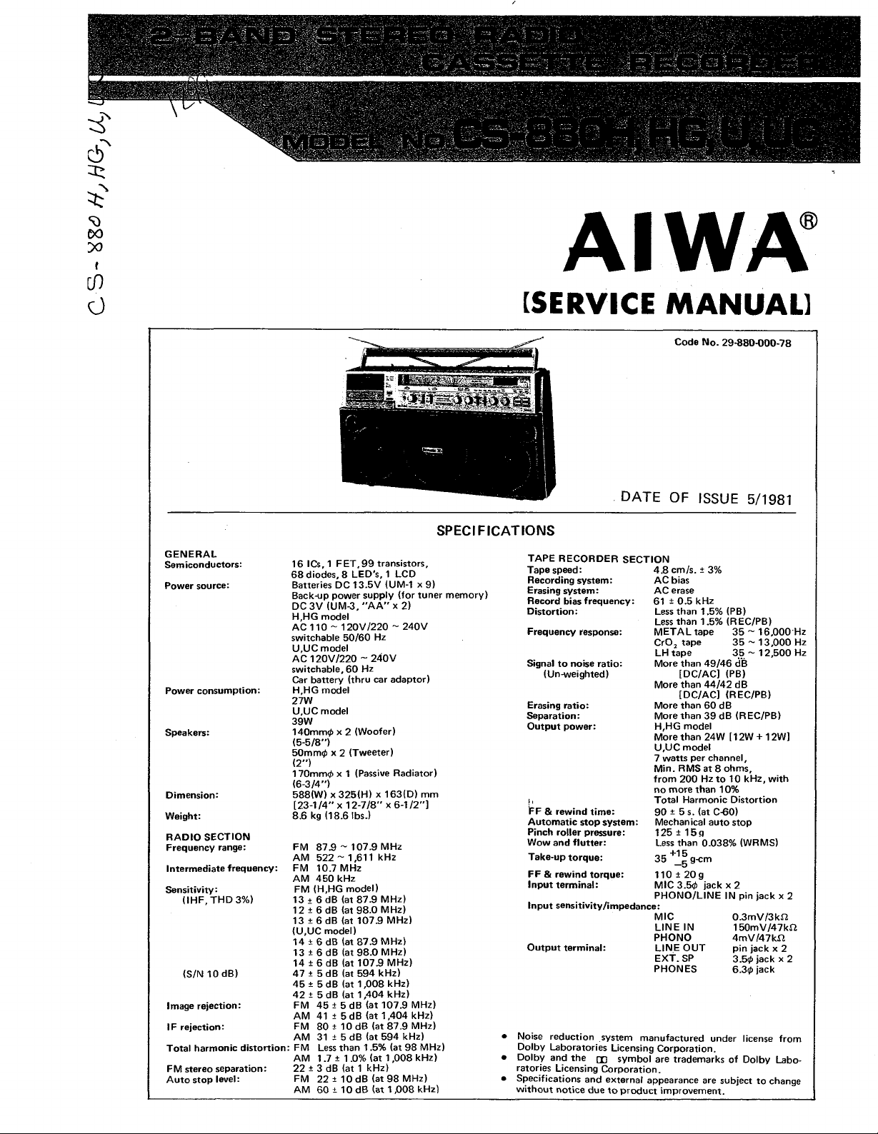
Page 1
à
's
AIWA
G S- H
[SERVICE MANUAL]
Code No. 29-880-000 -78
DATE OF ISSUE 5/1981
SPECIFICATIONS
GEN ER A L
Semiconductors:
Power source:
Power consumption:
Speakers:
Dimension:
Weight:
RAD IO SECTION
Frequency range:
Intermediate frequency:
Sen sitivity:
(IH F , THD 3%)
(S/N 10 dB) 47 ±5 dB
Image rejection: FM
IF rejection:
Total harmonic distortion:
FM stereo separation:
Auto stop level:
68 diodes, 8 LED's, 1 LCD
AC 110 ~ 120V/220 ~ 240V
switchable 50/60 Hz
switchable, 60 Hz
27W
39W
: FM
16 ICs, 1 FE T.9 9 transistors,
Batteries DC 13.5V (UM-1 x 9)
Back-up power supply (for tuner memory)
DC 3V (UM-3, "A A " x 2)
H,HG model
U,UC model
AC 120V/220 ~ 240V
Car battery (thru car adaptor)
H,HG model
U,UC model
14Omm0 x 2 (Woofer)
(5-5/8")
5Omm0 x 2 (Tweeter)
(2" )
17Omm0 x 1 (Passive Radiator)
(6-3/4” )
588(W) x 325(H) x 163(D) mm
[23-1/4" x 12-7/8" x 6-1/2")
8.6 kg (18.6 lbs.)
FM
875 ~ 107.9 MHz
AM
522 ~1,611 kHz
FM
10.7 MHz
AM
450 kHz
FM (H,HG model)
13 ± 6 dB (at 87.9 MHz)
12 ± 6 dB (at 98.0 MHz)
13 ± 6 dB (at 107.9 MHz)
(U,UC model)
14 ±6 dB
13 +
14 ±6 dB
45 ± 5 dB
42 ±
AM 41 ±
FM
AM 31 +
AM
22 ±3 dB
FM
AM
(at 87.9 MHz)
(at 98.0 MHz)
6 dB
(at 107.9 MHz)
(at 594 kHz)
(at 1,008 kHz)
(at 1,404 kHz)
5 dB
5 dB (at 107.9 MHz)
45 ±
5 dB (at 1,404 kHz)
10 dB (at 87.9 MHz)
80 ±
5 dB lat 594 kHz)
than 1.5% (at 98 MHz)
Less
1.0% (at 1,008 kHz)
1.7 ±
(at 1 kHz)
10 dB (at 98 MHz)
22 ±
10 dB (at 1,008 kHz)
60 ±
TA PE REC O RD ER SECT IO N
Tape speed: 4.8 cm/s. ± 3%
Recording system:
Erasing system:
Record bias frequency:
Distortion:
Frequency response:
Signal to noise ratio:
(Un-weighted)
Erasing ratio:
Separation:
Output power:
IFF & rewind time:
Automatic stop system:
Pinch roller pressure:
Wow and flutter:
Take-up torque:
FF & rewind torque:
Input terminal:
Input sensitivity /impedance:
Output terminal: LIN E O UT pin jack x 2
Noise reduction system manufactured under license from
Dolby Laboratories Licensing Corporation.
Dolby and the [Xj symbol are trademarks of Dolby Labo
ratories Licensing Corporation.
Specifications and external appearance are subject to change
without notice due to product improvement.
AC bias
AC erase
61 ± 0.5 kHz
Less than 1.5% (PB)
Less than 1.5% (R EC/PB)
METALtape 3 5 - 16,000 Hz
CrO j tape 35 ~ 13,000 Hz
LH tape 35 ~ 12,500 Hz
More than 49/46 dB
[DC/AC] (PB)
More than 44/42 dB
[DC/AC] (REC/PB)
More than 60 dB
More than 39 dB (REC /PB)
H,HG model
More than 24W [12W + 12W)
U,UC model
7 watts per channel,
Min. RM S at 8 ohms,
from 200 Hz to 10 kHz, with
no more than 10%
Total Harmonic Distortion
90 ±5 s. (atC-60)
Mechanical auto stop
125 ± 15q
Less than 0.038% (WRM S)
, , +15
35 c g-c m
-5
110 ± 2 0g
MIC 3.50 jack x 2
PHON O/LINE IN pin jack x 2
MIC 0.3mV/3kfi
LIN E IN 150mV/47kn
PHONO 4mV/47kii
EX T. SP 3.50 jack x 2
PHONES 6.30 jack
Page 2
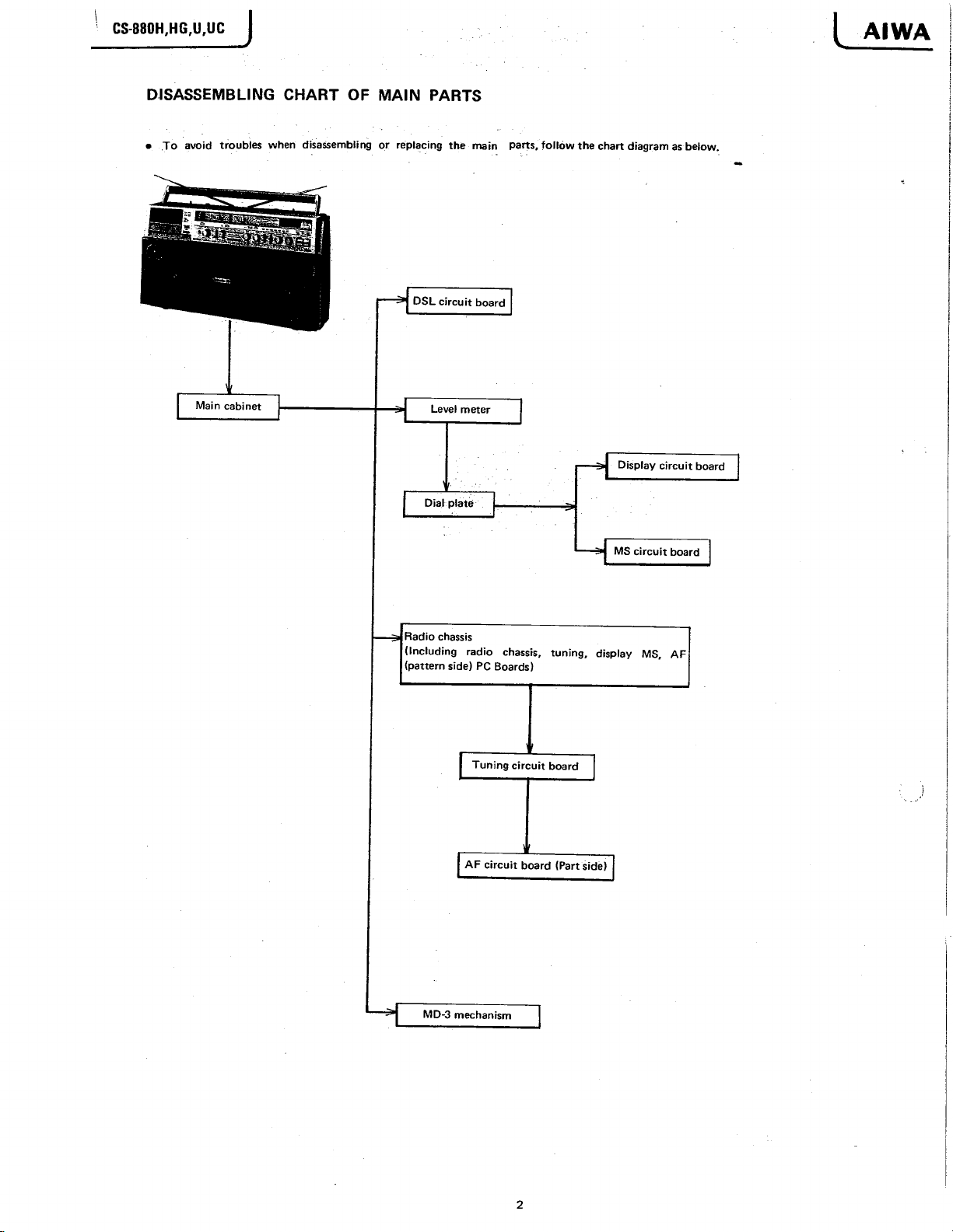
CS-880H
,HG,U,UC
DISASSEMBLING CHART OF MAIN PARTS
To avoid troubles when disassembling or replacing the main parts, follow the chart diagram as below.
L AIWA
Radio chassis
(Including radio chassis, tuning, display MS, A f |
{pattern side) PC Boards)
Tuning circuit board
A F circuit board (Part side) i
MD-3 mechanism
2
Page 3
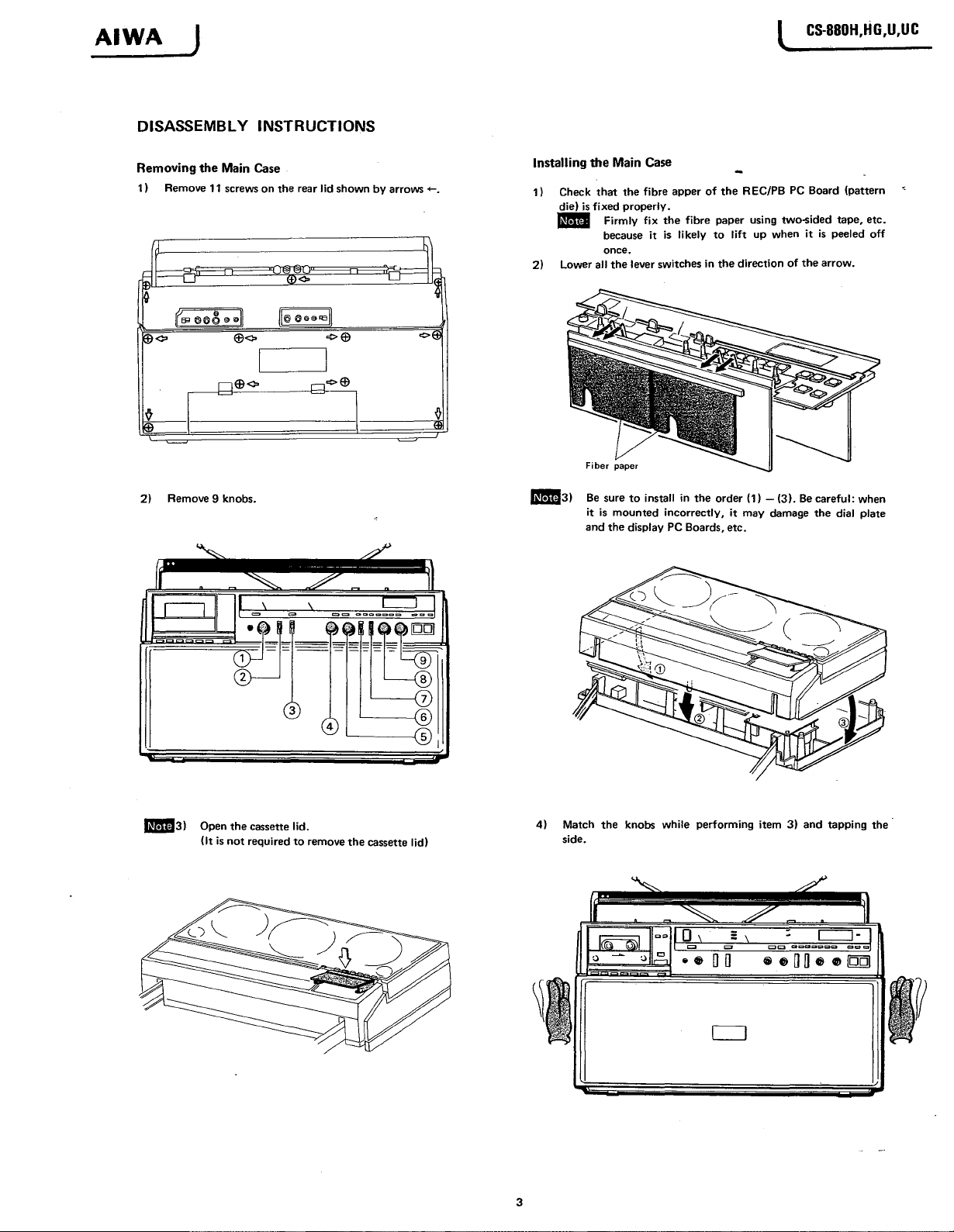
AIWA J
DISASSEMBLY INSTRUCTIONS
CS-880H,HG,U,UC
Removing the Main Case
1) Remove 11 screws on the rear lid shown by arrows <
-----
— Ö 1-
© o
- Q
2) Remove 9 knobs.
-
rO§"©On
________
-
©<= ”
j—
-
°v=Cj -
-
“□
Installing the Main Case
1) Check that the fibre apper o f the REC/PB PC Board (pattern
die) is fixed properly.
Firmly fix the fibre paper using two-sided tape, etc.
because it is likely to lift up when it is peeled off
once.
2) Lower all the lever switches in the direction of the arrow.
5 0 3 ) Be sure to install in the order (1) — (3). Be careful: when
it is mounted incorrectly, it may damage the dial plate
and the display PC Boards, etc.
S g 3 ) Open the cassette lid.
(It is not required to remove the cassette lid)
4) Match the knobs while performing item 3) and tapping the
side.
3
Page 4
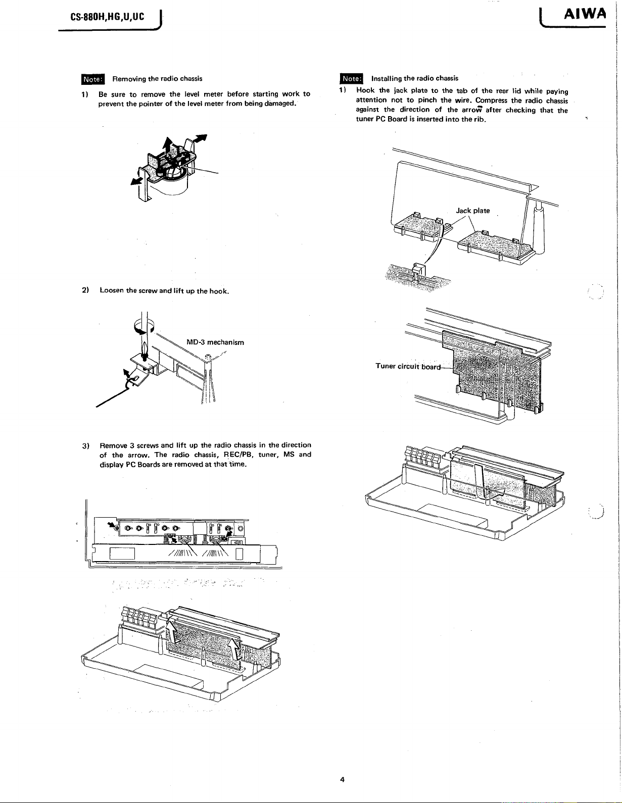
CS-880H,HG,U,UC
J
AIWA
L
Removing the radio chassis
1) Be sure to remove the level meter before starting work to
prevent the pointer of the level meter from being damaged.
Installing the radio chassis
1) Hook the jack plate to the tab of the rear lid while paying
attention not to pinch the wire. Compress the radio chassis
against the direction of the arrow after checking that the
tuner PC Board is inserted into the rib.
4
Page 5
AIWA I
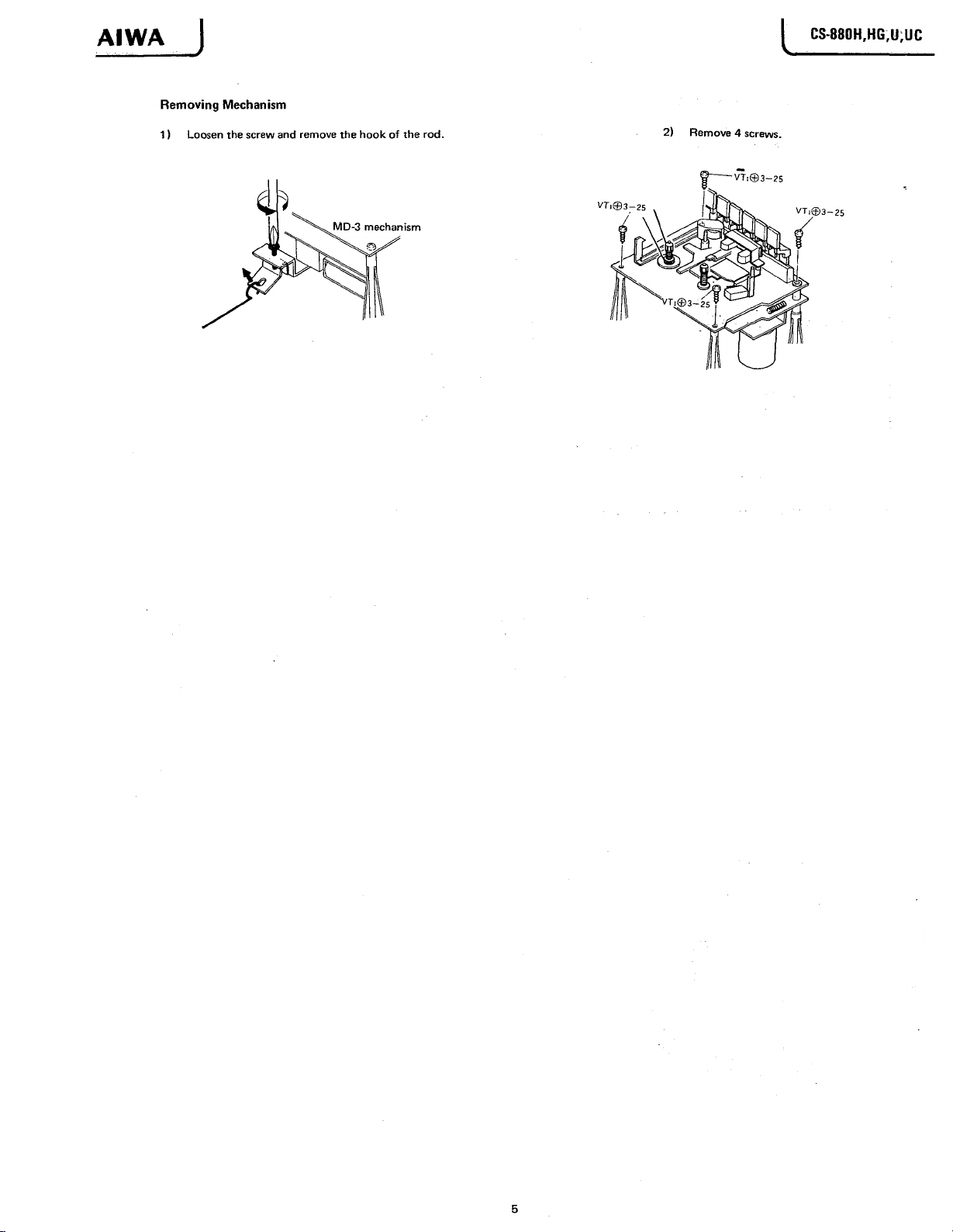
Removing Mechanism
CS-880H,HG,U;UC
1) Loosen the screw and remove the hook of the rod.
2) Remove 4 screws.
5
Page 6
CS-880H,HG,U,UC
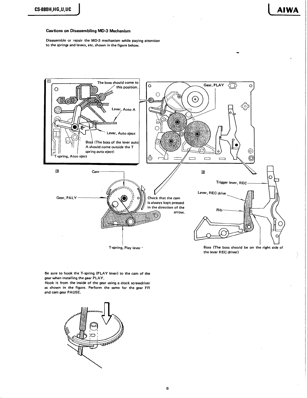
Cautions on Disassembling MD-3 Mechanism
Disassemble or repair the MD-3 mechanism while paying attention
to the springs and levers, etc. shown in the figure below.
1 AIWA
Be sure to hook the T-spring (P LA Y lever) to the cam of the
gear when installing the gear P LA Y .
Hook it from the inside of the gear using a clock screwdriver
as shown in the figure. Perform the same for the gear FR
and cam gear P AU SE .
the lever RE C driver)
6
Page 7
AIWA
J
DESCRIPTION OF THE MD-3 MECHANISM
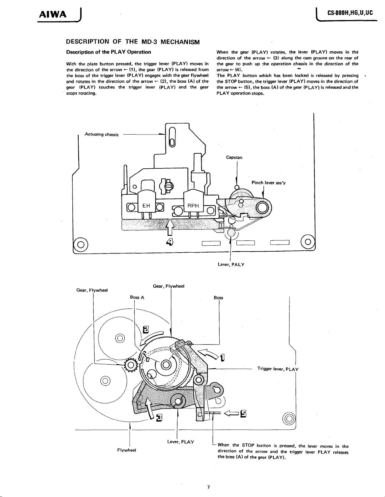
Description of the PLAY Operation
With the plate button pressed, the trigger lever (P LAY) moves in
the direction of the arrow «- (1), the gear (P LA Y ) is released from
the boss of the trigger lever (P LA Y ) engages w ith the gear flywheel
and rotates in the direction of the arrow ■*- (2), the boss (A) of the
gear (P L A Y ) touches the trigger lever (P LA Y ) and the gear
stops rotating.
CS-880H,HG,U,UC
When the gear (P L A Y ) rotates, the lever (P L A Y ) moves in the
direction of the arrow •*- (3) along the cam groove on the rear of
the gear to push up the operation chassis in the direction of the
arrow <-(4). **
The P LA Y button which has been locked is released by pressing
the STOP button, the trigger lever (P LAY) moves in the direction of
the arrow *- (5), the boss (A ) of the gear (P LA Ÿ ) is released and the
PL A Y operation stops.
the boss (A ) of the gear (PLA Y ).
Page 8
CS-880H,HG,U,UC
J
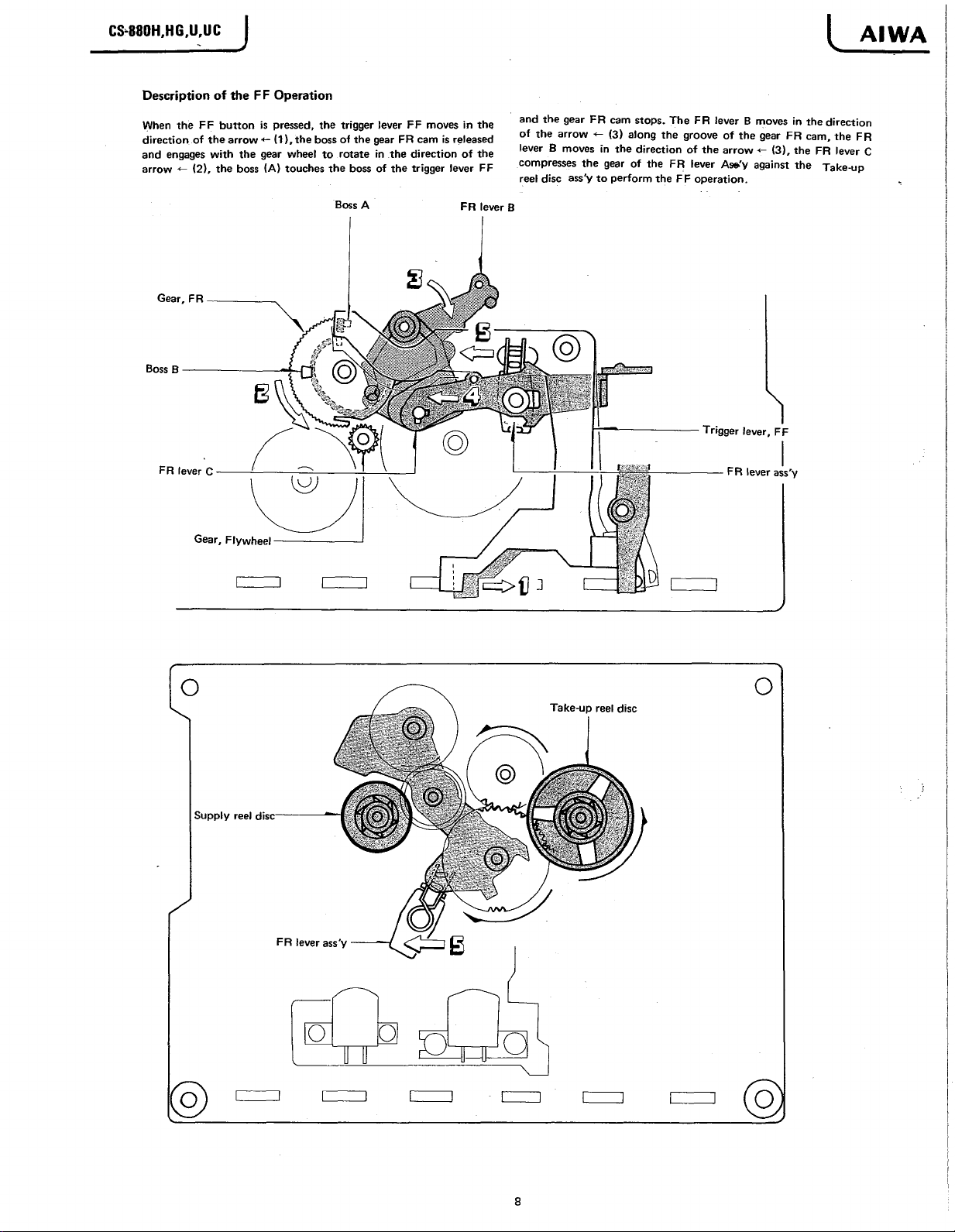
Description of the FF Operation
When the FF button is pressed, the trigger lever F F moves in the
direction of the arrow *- (1 ), the boss of the gear FR cam is released
and engages with the gear wheel to rotate in the direction of the
arrow < - (2), the boss (A ) touches the boss of the trigger lever FF
AIWA
and the gear F R cam stops. The F R lever B moves in the direction
of the arrow < - (3) along the groove of the gear FR cam, the FR
lever B moves in the direction of the arrow «- (3 ), the F R lever C
compresses the gear of the F R lever A » 'y against the Take-up
reel disc ass'y to perform the FF operation.
Boss A
FR lever B
8
Page 9
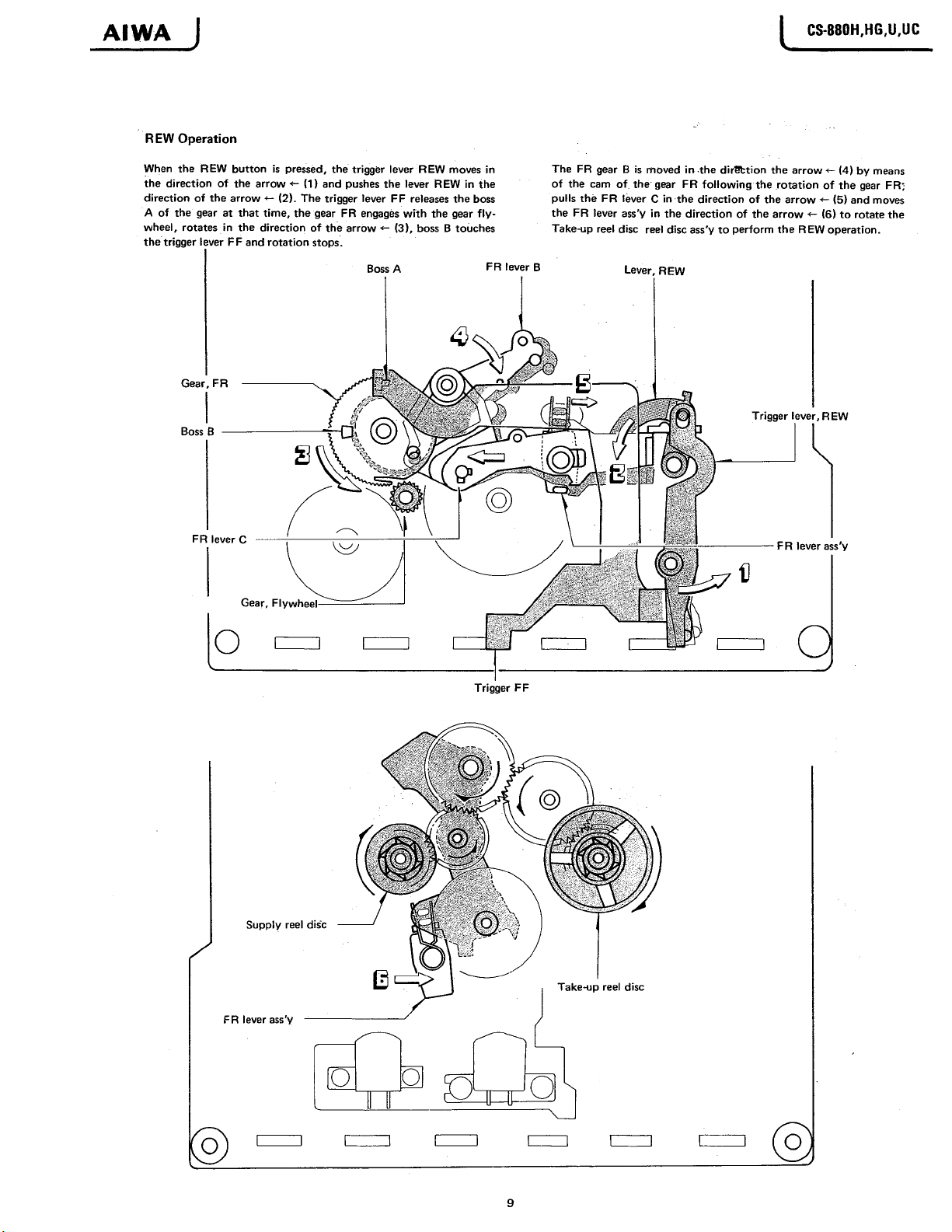
AIWA
REW Operation
J
[ CS-880H.HG.il.UC
When the RE W button is pressed, the trigger lever REW moves in
the direction of the arrow < - (1) and pushes the lever REW in the
direction of the arrow < - (2). The trigger lever F F releases the boss
A of the gear at that time, the gear FR engages w ith the gear fly
wheel, rotates in the direction of the arrow <- (3), boss B touches
the trigger lever FF and rotation stops.
The FR gear B is moved in the dirSfction the arrow < - (4) by means
of the cam of the gear F R following the rotation of the gear F R;
pulls thè F R lever C in the direction of the arrow < - (5) and moves
the FR lever ass’y in the direction of the arrow ■*- (6) to rotate the
Take-up reel disc reel disc ass'y to perform the REW operation.
9
Page 10
CS-880H,H6,U,UC
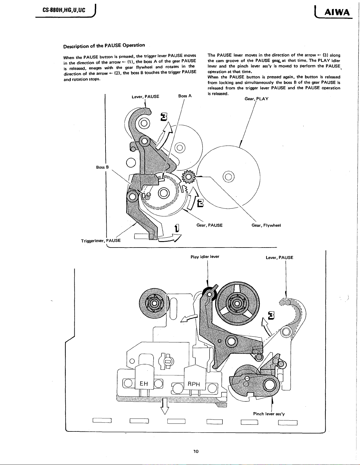
Description of the PAUSE Operation
When the P AUS E button is pressed, the trigger lever PA U SE moves
in the direction of the arrow +- (1), the boss A of the gear PA USE
is released, enages with the gear flywheel and rotates in the
direction of the arrow - (2), the boss B touches the trigger P AUSE
and rotation stops.
J I AIWA
The PAUSE lever moves in the direction of the arrow *- (3) along
the cam groove of the PAUSE g e ^ a t that tim e. The P LA Y idler
lever and the pinch lever ass'y is moved to perform the P AUSE
operation at that tim e.
When the P AUS E button is pressed again, the button is released
from locking and simultaneously the boss B of the gear PA U SE is
released from the trigger lever P AUS E and the PA US E operation
Play idler lever Lever, PA U SE
10
Page 11
AIWA
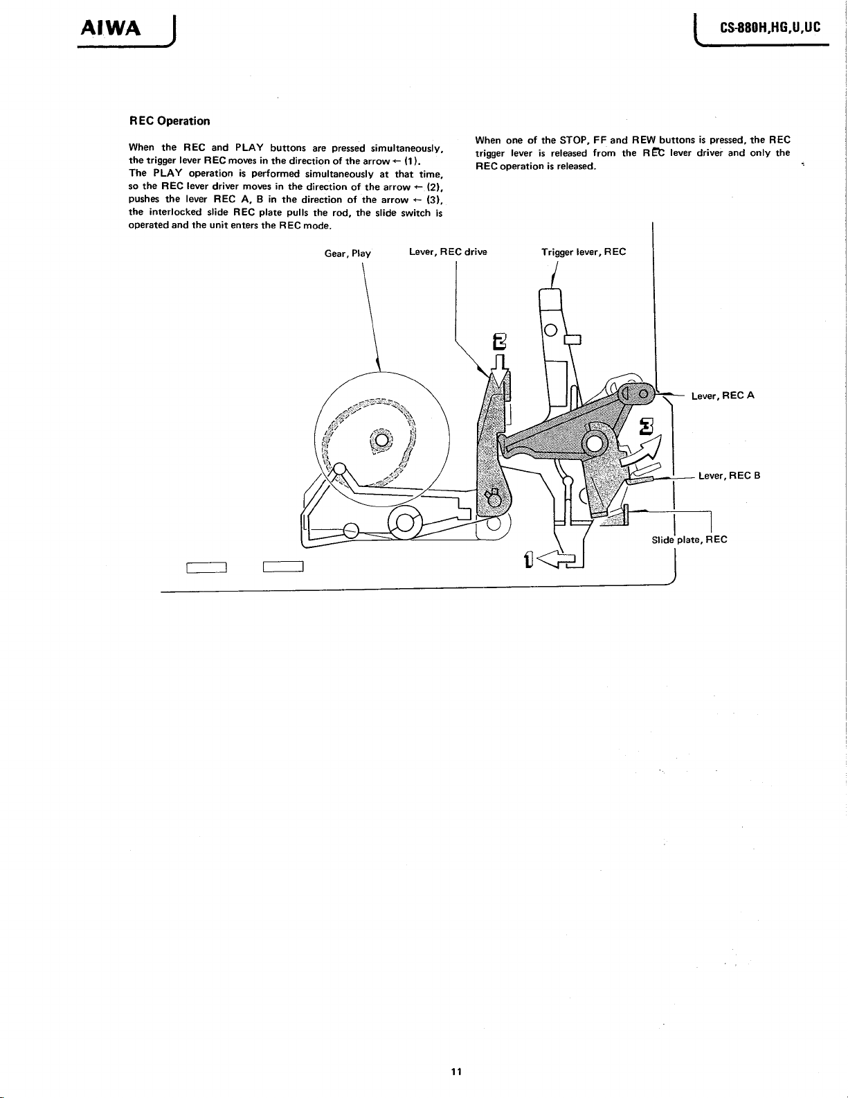
R EC Operation
When the REC and PL A Y buttons are pressed simultaneously. trjgger |ever js re|eased from the R Ê t ,ever driver and on|y the
the trigger lever RE C moves in the direction of the arrow - (1 ). REC operation is released.
The PL A Y operation is performed simultaneously at that time,
so the R EC lever driver moves in the direction of the arrow <-.(2),
pushes the lever REC A , B in the direction of the arrow (3),
the interlocked slide RE C plate pulls the rod, the slide switch is
J
CS-880H,HG,U,UC
When one of the STOP, FF and R E W buttons is pressed, the REC
11
Page 12
CS-880H,HG,U,UC
J
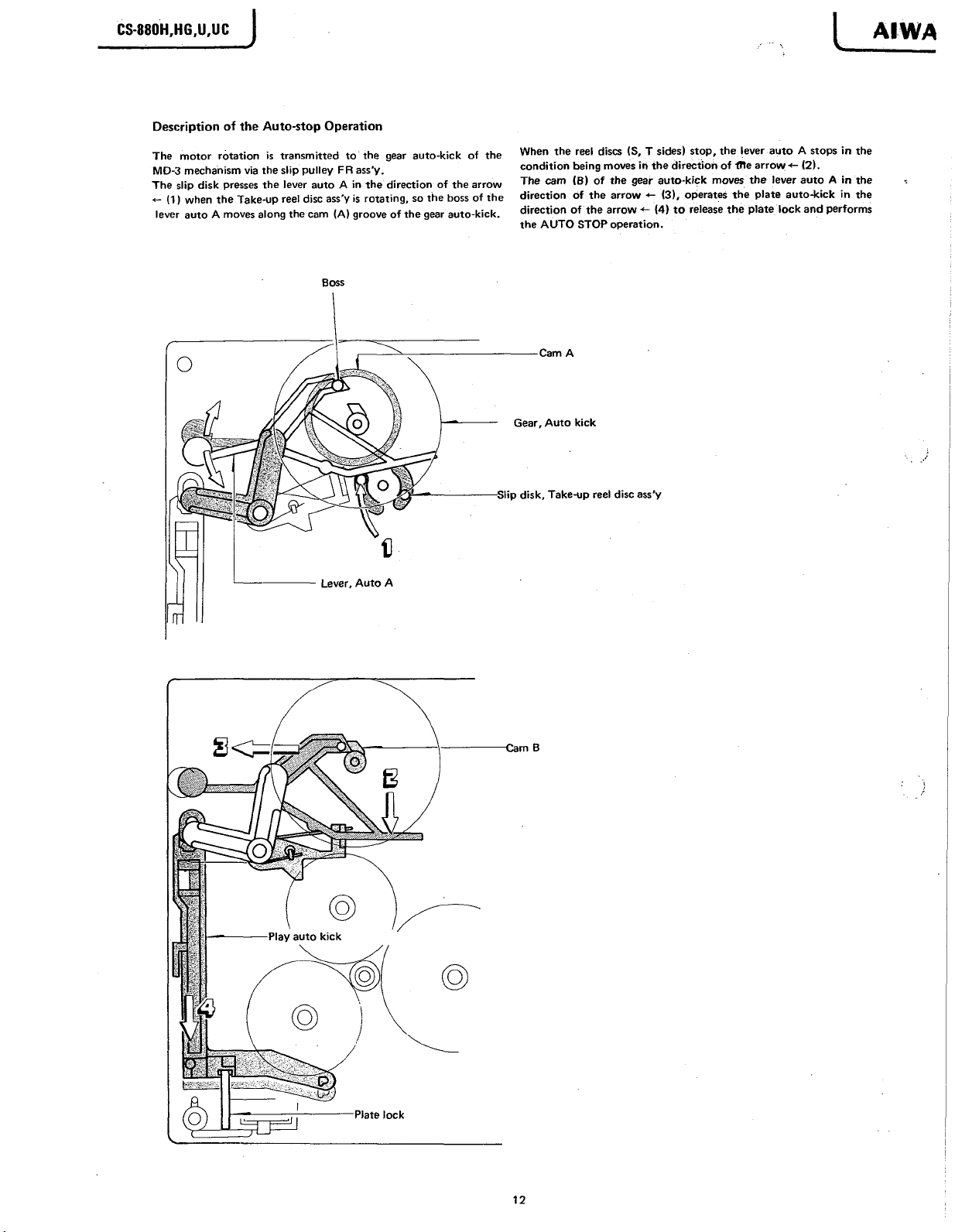
Description of the Auto-stop Operation
The motor rotation is transmitted to the gear auto-kick of the
MD-3 mechanism via the slip pulley FR ass’y.
The slip disk presses the lever auto A in the direction of the arrow
<- (1) when the Take-up reel disc ass'y is rotating, so the boss of the
lever auto A moves along the cam (A ) groove of the gear auto-kick.
Boss
I
When the reel discs (S, T sides) stop, the lever auto A stops in the
condition being moves in the direction of flle arrow (2).
The cam (B ) of the gear auto-kick moves the lever auto A in the
direction of the arrow <- (3 ), operates the plate auto-kick in the
direction of the arrow <- (4) to release the plate lock and performs
the AU TO ST OP operation.
AIWA
12
Page 13

AIWA
SPRING APPLICATION POSITION
J
CS-880H,HG,U,UC
13
Page 14

CS-880H,HG,U,UC j
AIWA
EXPLODED VIEW—1
1 I 2
B
3 I 4 I 5
7
H
14
Page 15

AIWA j
MECHANICAL PARTS
Ref. No. Part No.
1 - 1 a 09-01 7-8 39 -01
1-1 b
1-2
1 - 3 82-5 87 -22 7- 01
1-4 82- 576 -2 41- 01
1- 5 8 2- 58 7-0 20 -01
1-6
1- 7 8 2- 58 7-2 18 -01
1-8 82 -58 7- 202 -0 1
1- 9a 82-58 7-0 04 -0 1
1-9 b 82- 58 7- 04 7-0 1
1-1 0
1-11
1-1 2
1- 13a 09 -01 7-8 41 -01
1- 1 3b 0 9-0 17 -84 2- 01
1- 14
1-1 5
1-1 6 82- 58 7-2 31 -0 1
1- 17 82 -58 7- 233 -0 1
1-1 8
1-1 9 82 -5 87- 208 -0 1
1-2 0
1-21
1-2 2
1- 2 3 82- 587 -0 05- 01
1-2 4
1-25 a
1-25 b
1- 2 6 82- 587 -0 17- 01
1- 2 7
1-28
1-2 9 82 -58 7- 024 -0 1
1-30 a 82-58 7- 02 9- 01
1-30b 82-5 87- 03 3- 01
1-30C
1-31 a 82-5 87 -0 25 -0 1
1-31b
1-3 1 C
1-31 d
PARTS LIST
Part No.
Changed to
Main case ass’y (Silver)
(H ,U ,U C model only)
09-0 17 -8 40 -01
82-58 7 -00 1 -0 1
82-5 8 7-04 4 -0 1
82-58 7 -23 4 -0 1
82-5 8 7-23 5 -0 1
82 -5 8 7-0 07 -0 t
82 - 5 87-0 4 5-01
82-58 7 -03 6 -0 1
82 - 5 87-0 6 0-01
82-5 8 7-00 9 -0 1
82 - 5 87-0 1 0-01
82-5 8 7-02 7 -0 1
82 -5 6 3-03 2 - 0 1
82-5 8 7-00 3 -0 1
82-5 8 7-22 1 -0 1
82 - 5 87-0 4 0-01
82-5 8 7-23 9 -0 1
87 - 3 92-0 0 3-01
87-3 2 1-09 7 -2 1
82-5 87 -63 5- 01
Main case ass'y (Blue)
Cabinet, Main (Silver)
Cabinet, Main (Blue)
Damper A , Rubber
Damper B, Rubber
Panching (Silver)
Panching (Blue)
Badge (Stiver)
Badge (Blue)
Side panel R
Sid e p a nel L
Panel, Front
Cassette plate
Window, Dial
E-spring (tact)
Label, D S L
P-spring , T act A
Nut, Speed
Q T , + 3 - 1 2
Drone cone ass'y
P-spring, Earth
E-spring, Earth CS-350
Ta c t push-key
82-5 87- 021 - 01
Push-button
T-spring, Cassette lid
Cassette box
Window, Cassette (Silver)
(H ,U ,U C model only)
Window, Cassette (Blue)
82-5 87 -01 1- 01
87-0 81 -97 9- 01
82-5 87 -21 9- 01
Decorative panel. Cassette
Decorative screw 3-12
P-spring, Cassette holder
Back cover ass'y (H ,HG model only)
Back cover ass'y (U ,U C model only)
82 - 5 87-03 8 -0 1
82-5 8 7-04 2 -0 1
82 - 5 87-23 6 -0 1
82-5 8 7-21 3 -0 1
82-5 8 7-21 4 -0 1
82-5 8 7-21 6 -0 1
82-5 8 7-21 5 -0 1
82-5 8 7-21 7 -0 1
82-5 8 7-22 6 -0 1
82-2 7 7-38 2 -0 1
81-2 3 5-21 1 -0 1
87-3 4 9-09 5 -2 1
82-5 34 -20 3- 01
82-5 87 -21 2- 01
Back co v e r as s'y (H,H G m od e l on ly)
Back cov e r as s'y (U,UC m o d el on ly )
Rubber cushion 4-6 - 4
C-spring, T erm inal A
C-spring, Terminal B
C-spring, Terminal C
Terminal plate U,
Terminal plate U3
Sheet, Faiber
Spring, Terminal
Terminal plate D
U T , + 3 - 8
Click plate spring R
Shaft, Handle
Rubber bushing 6 x10
Rubber bushing 7 x1 0
87-0 38 -03 9- 01
Wire binder
Rubber bushing 3 x5
82-5 87 -01 3- 01
82-5 87- 01 4-0 1
82-5 87 -01 2- 01
Handle L *
Handle grip
Handle R
Battery room lid
82-5 87 -23 7- 01
82-5 87- 211 -0 1
82-5 88 -22 3- 01
M cushion 14 x 35 x 5
Cushion, Battery (H,HG model only)
M cushion 7 x 281 x 7
Knob
82-5 63 -01 4- 01
82-5 87 -0 23 -0 1
Knob, TO G G LE
Knob, V OLUM E (U P)
Knob, V O LU M E (DOWN)
Name plate. Spec. (H model only)
Name plate. Spec. (HG model only)
82-5 87 -03 2- 01
Name plate. Spec. (U,UC model only)
AC jack plate (H,HG model only)
82-5 87 -0 26 -0 1
AC jack plate (U ,U C model only)
82-5 87 -03 4- 01 AC jack plate S-1 (UC model only)
82-5 87 -03 5- 01 AC jack plate S-2 (U ,U C model only)
................
Description
- ■ —
CS-880H,HG,U,UC
I
1 mark in this part list shows exclusive part.
Common
Model
*
*
* «•
•
•
* 1
•
*
•
* 1.
*
•
CS-990 1
*
•
»
*
*
•
*
*
*
*
*
*
*
*
*
■ft
*
•
*
•
*
•
*
*
*
*
*
»
* 1
*
*
CS-770 2
*
CS-990
*
*
*
*
*
*
*
*
*
Q'ty
1
1
1
1
14
1
1
1
1
1
1
1
1
1
1
1
12
1
1
1
1
1
1
1
1
1
1
1
1
1
1
1
1
1
1
1
1
1
1
1
1
1
2
4
4
1
1
1
1
1
1
1
1
1
?
Page 16

CS-880H,HG,
uj u
EXPLODED VIEW —2
1 I 2
B
H
16
Page 17

AIWA
J
CS880H;HG,U,UC
Ref. No.
2 - 1
2- 2
2- 3
2- 4 82-587 -20 5- 01
2- 5
2- 6
2- 7
2- 8
2- 9
2-10
2- 1 1
2-1 2
2-1 3
2-1 4
2-15
2-1 6a
2-1 6b
2-1 6c 82-587- 06 2- 01
2-1 7
2-18
2-19
2-20
2- 2 1
2-22
2-2 3
2-2 4
2-25
2-2 6
2-2 7
2-28
2-29
2-30
2- 3 1
Part No.
87-0 43 -0 58 -01
87-0 33 -1 66 -01
82-5 87 -2 20 -0 1
82-5 88 -2 09 -01
82-5 87 -24 2- 01
82-5 87 -2 11 -01
82-5 87 -22 5- 01
82-5 87 -2 06 -01
82-5 87 -60 8- 01
82-5 87 -2 38 -0 1
82-5 87 -2 01 -01 Chassis
82-5 87 -2 07 -01
82-1 62 -03 7- 01
82-5 88 -63 4- 01
82-5 87 -0 08 -01 Dial plate (Silver)
82-5 87 -06 1- 01
87- 06 4-0 84 -0 1
82-5 87 -01 9- 01 Push-key, R EC mute
82- 56 3- 24 7-0 1
87-0 96 -04 5- 01
87-0 78 -0 03 -01
82-5 87 -24 0- 01
82- 58 7- 22 4-0 1
87-0 40 -1 43 -01
82-5 87 -20 9- 01
82-5 87 -2 03 -01
82-5 87 -0 37 -01 Push-key, REC
82- 58 7- 01 8-0 1
82-5 88 -2 08 -01
87-0 63 -11 3- 01
82- 58 7- 04 9-0 1
Part No.
Changed to
Description
Whip antenna 2
Antenna terminal
Terminal plate. Antenna
Rod, REC
Cushion 15 x 15 x 41 CS-770 1
Sheet, Fiber A
Cushion, Battery
Rod 37.8
Rod 87.8
Shield, Front
Rubber cushion 10 x 25 x 14
Holder, Dial plate
Push-button B 2
Earth, R EC
(H,U,UC model only)
Dial plate (Blue)
(H,HG model only)
Dial plate (Blue)
(U ,U C model only)
Holder , ECM 30 2
E-spring, Air-damp
String, Dial
Air-damp unit ass'y
LED reflector
Holder, Switch
Counter
Rubber belt
Holder, Counter
Push-key, Tape recorder
Rubber cushion 33-6 - 3 CS-770 1
Cushion W A 2
Push-button, D SL
Common
Model
*
•
•
*
•
*
*
•
*
*
ÀD-R500
CS-770 1
*
*
*
*
CS-990 1
*
*
*
*
*
*
*
Q'ty
H,U,UC:4
HG:3
2
2
1
2
1
1
2
1
1
1
2
1
1
1
1
1
1
1
1
1
1
1
1
5
1
17
Page 18

CS-880H,HG,U,UC
EX PLO D E D VIE W —3
1 I 2
B
PW I.7-3.5 -0.25
J
[ AIWA
U 0 2-I2
PW I.7-3.5~0.25
H
PW I.7-3.5-0.25
18
Page 19

AIWA
J
CS-880H,H6,U,UC
Re f. N o. Part No.
3 - 1 82-58 5- 32 5-0 1
3- 2 82-5 85 -2 77 -01
3- 3
3- 4 82-585 -27 9- 01
3- 5 82-585 -25 5- 01
3- 6 82-5 85 -31 9- 01
3- 7 82-5 85 -25 4- 01
3- 8 82-585 -31 1- 01
3- 9 82-585 -29 0- 01
3-10
3- 1 1 82-5 85 -2 92 -01
3-12
3-13 8 2- 585 -2 10- 01
3-14 82 -58 5- 29 4- 01
3-15 8 2-5 85 -3 12 -0 1
3-16
3-1 7 82-58 5- 28 6- 01
3-18 82 -58 5- 25 2- 01
3-19 8 2-5 85 -2 65 -01
3-20
3- 2 1
3-22 8 2-5 85 -2 23 -01
3-2 3 82 -58 5- 313 -0 1
3-24 82 -58 5- 36 4- 01
3-25
3-26
3-27 8 2-5 85 -3 38 -01
3-28
3-29 8 2- 585 -2 08- 01
3-30
3- 3 1 82-585 -2 91 -01
3-32
3-33
3-34 82 -5 85 -2 84 -01
3-35
82-5 85 -3 37 -01
82-5 85 -2 15 -01
82-5 85 -2 72 -01
82-5 85 -25 3- 01
82-5 85 -23 1- 01
82-5 85 -23 5- 01
82-5 85 -29 6- 01
82- 58 5-3 40 -0 1
82- 58 5- 29 5-0 1
82-5 85 -20 9- 01
82-5 88 -6 28 -0 1
87-0 73 -00 5- 01
87-0 38 -0 56 -0 1 Wire binder
Part No.
Changed to
Description
Outsert chassis 1
Plate button, F R 3
Plate button, R EC 3
Lever A , Eject
REC blocking lever 1
P-spring, Cassette pressure 1
Slide plate. Eject 1
E-spring, Lid lock 1
C-spring, Back tension 1
Supply reel platform ass'y 1
C-spring, Slip disk 1
Slip disk T 1
Take-up reel platform ass'y 1
T-spring, Center shift
E-spring, Brake R
Lever, Brake R 1
Rubber cushion. Brake
Lever, Brake L 1
REV lever 1
F R lever ass'y 1
Gear A, REW 1
Play idler lever ass’y
F-spring, Play idler
Pinch lever B ass'y 1
T-spring, Pinch lever
Plate lock ass'y 1
Rubber cushion. Play lever
T-spring. Actuating
Actuating chassis
Head base 1
C-spring, RPH
Shield plate
Steel ball 20 1
P-spring, Actuating
Common
Model
CS-770
Q'ty
1
1
1
1
1
1
1
1
1
1
1
1
1
19
Page 20

CS-880H.HG,
EXPLODED VIEW—4
B
uuc I
___!
___I___
{ AIWA
L
V © 3-I2
f^ V T T ® 2 .6 -5
PW 2.1-3.5-0.25
H
20
32
Page 21

CS880H,HG,U,UC
Ref. No. Part No.
4 -1
4- 2 82-585- 28 5-0 1
4- 3 82-585- 31 7-0 1
4- 4 82-585- 30 6-0 1
4-5 82-58 5- 283 -0 1
4- 6
4- 7 82- 585 -3 27- 01
4-8 82-58 5- 268 -0 1
4- 9 82-585- 26 9-0 1
4-10 82-58 5-2 70 -01
4- 1 1 82-585 -24 8-0 1
4-12 82-58 5-2 64 -01
4-13 82-58 5-2 97 -01
4-14
4-15 82-585-29901
4-16 82-5 85- 26 2-0 1
4-17
4-18 82-5 85- 29 8-0 1
4-19 82-58 5-2 61 -01
4-20
4- 2 1 82-585 -3 03- 01
4-22 82-58 5-3 08 -01
4-23 82-58 5-3 41 -01
4-24 82-58 5-3 00 -01
4-25 82-58 5-2 17 -01
4-26 82-58 5-2 16 -01
4-27
4-28 82-58 5-2 45 -01
4-29 82-5 85- 25 6-0 1
4-30 82-5 85- 30 4-0 1
4- 3 1
4-3 2 82-585- 24 7-0 1
4-3 3 82-585- 24 9-0 1
4-34
4-35 82-5 85- 30 7-0 1
4-3 6 82-585- 26 6-0 1
4-3 7
4-38 82-5 85- 31 4-0 1
4-3 9 82-585- 25 8-0 1
4-40
4- 4 1 82-585 -3 08- 01
4-4 2 82-585- 33 1-0 1
4-43 82-58 5-2 57 -01
4-44 82-5 85- 30 1-0 1
4-45 82-5 85- 32 1-0 1
4-4 6 82-58 5-2 03- 01 Mechanism chassis B ass'y
4-4 7
4-48 82-5 85- 33 2-0 1
4-49 82-5 85- 22 9-0 1
4-50 82-5 85 -24 3-0 1
4- 5 1
4-52 82-58 5-3 36 -01
4-53 82-58 5-2 87 -01
4-54
4-55 82-58 5- 281 -0 1
4-56 82-58 5- 242 -0 1
4-5 7
4-58
4-5 9 87- 038 -0 39- 01
4-60 82-58 7-2 41 -01
4- 6 1
4-6 2 82-585 -3 35- 01
4-6 3
4-6 4
4-65
4-66 82-587- 23 2-0 1
82-5 85 -2 89 -0 1
82- 585 -2 82- 01
82-5 85 -27 1- 01
82-5 85 -26 3- 01
82-5 85 -26 0- 01
82-5 85 -24 4- 01
82-5 85 -24 6- 01
82-5 85 -25 0- 01
82-5 85 -26 7- 01
82-5 85 -25 9- 01
82-5 85- 31 5-0 1
82-5 85- 32 4-0 1
82-5 85- 32 3-0 1
82- 585 -3 26- 01
82-5 88 -20 6- 01
82-5 87- 228 -0 1
87-0 87- 029 -0 1
87-0 81- 483 -0 1
82-5 85 -3 42 -01
Part No.
Changed to
Shaft lock
C-spring lock 1
E-spring, Button lock
T-spring, Play lever
Slid e plate, FR auto
Slid e plate. Motor switch
Slide plate key ass'y
Auto A lever
Auto B lever
Plate auto kick 1
Lever, PA USE 1
FR lever D 1
T-spring, FR lever A
Auto eject lever
T-spring, Auto eject 1
F R lever B 1
F R lever C 1
T-spring, FR lever B 1
Trigger lever, REC 1
Lever, REW 1
T-spring, Trigger (R EC ) 1
E-spring, R EW lever 1
E-spring, FR lever 1
T-spring, F R cam 1
Slip pulley F R ass'y
Drive gear 1
Play cam gear
F R cam gear
Trigger lever, PA USE
T-spring, Trigger (PA U SE) 1
Gear, PA U SE 1
Gear, Auto kick 1
PL A Y lever
Lever, REC drive 1
T-spring, RE C lever 1
REC A lever 1
REC B lever
E-spring, REC
Trigger lever, PL A Y
Trigger lever, REW 1
T-spring, RE W lever 1
C-spring, R EW lever 1
FF trigger lever
E-spring, Trigger P LA Y
T-spring, Auto kick
E-spring, Slide plate 1
E-spring, REC lock 1
Flyw heel ass’y
Gear, Flywheel 1
C-spring, Flywheel 1
Rubber belt F R B
Rubber belt. Flyw heel
Holder, Pause switch 1
Holder, Motor
Motor pulley 1
Thrust bearing B
Rubber cushion, REC lever
Wire binder
E-spring, Slide plate
Slide plate R EC ass'y
T-spring, Plate lock
Rubber cushion
Motor screw, M2.6
Rubber cushion, P AU SE lock
Holder, REC switch
Description
Common
Model
-
CS-770 1
*
*
*
Q'ty
1
1
1
1
1
1
1
1
1
1
1
1
1
1
1
1
1
1
1
1
1
1
1
1
1
1
1
1
1
1
1
21
Page 22

CS-880H,HG,U,UC
- «
Description of Circuitry
1. Block Diagram of Synthesizer Tuner
ROD ANTENNA
EXT. O -lf.
ANTENNA
TERM INALS O -
[ AIWA
2. Outline of PLL Frequency Synthesizer
The P L L (phase-locked loop) requency synthesizer is a cirucit
which uses the extremely stable frequency of a crystal oscillator
as the reference signal to produce the frequencies desired. For
instance, to pick up a station broadcasting on a frequency of
100 MHz, a local oscillation frequency (fD : output frequency of
voltage-controlled oscillator) supplied to the mixer of 110.7 MHz
(100+ 10.7) is required. This particular unit adopts a prescaler
which employs a pulse swallow system to divide the frequency,
and send it to the programmable counter inside the controller
IC. The output frequency fn then enters the phase comparator.
The frequency of the extremely stable 4 5 MHz crystal oscillator
is counted down (1/180) at the same time and the reference
frequency fref of 25 kHz is sent to the phase comparator. The
phases of fn and fref are compared and the difference between
the two is detected. If there is no difference, the loop is locked;
if there is a difference, the control voltage passes through the
low-pass filter, it is fed out to the VCO and the VCO is con
trolled until fn is made equivalent to 25 kHz.
The reference frequency fref for AM reception is 9 kHz (or 10
kHz). The VCO frequency signal is sent directly to the pro
grammable counter.
CRYSTA L
OSCILLATOR 4.5MH1
V. C.O :V O L T « E CONTROLLED OSCILLATOR
Fig. 2
2-1 . Operation During FM Reception
The pulse swallow system is first outlined.
The relationship between fosc and fref is expressed as:
^osc= N ^ ^ r e f............................................................ (1)
If N is assumed to be P notation:
fosc = (ni +Pn2 + P2 n3 +
= P (n, /P + n2 + Pn3 + . . . . + Pn _ 2 nn) f ref
If, now, the part including the second digit and above is made Np:
fosc = p (ni/ p + N P) fref
This is modulated to become:
fosc = <ni + PNp + Pn, — Pnt ) fref
= [(N p — n ,) P + n, (P + 1 )] f ref
The above represents the principle of the pulse swallow system.
In order to achieve the relationship expressed in formula (2) by
physical means, this unit has a prescaler with two frequency
division ratios, 1/16and 1/17. In formula (1 ), this corresponds to
P = 16. Actual operation is as follows: when the signal produced
by dividing fosc by (P + 1 ) is counted down n, times at the first
programmable divider digit and nx becomes 0, the P-divided
signal is counted down (Np — n, ) times equivalent to the number
of the first digit subtracted from the number of the second and
higher digits of the programmable divider, and the cycle ends.
This cycle is performed with fref equal to 25 kHz.
When fs = 100 MHz is received:
f|F is 10.7 MHz and so therefore fosc = 100 + 10.7 = 110.7 MHz
From formula (1 ): N = ^ = 4428
If this figure is re-expressed in the sexadecimal notation, and
made to correspond with 114C formula (2 ):
Np = 114, n, = C
Therefore, fref x [(114 — C) x 10 + C x 11 ] = fosc
If this is re-expressed in the decimal notation:
25 kHz x [(1 62 + 161 + 4 - 12) x 16+ 12 x 17] = 110.7 MHz
What happens is that the prescaler divides the frequency by 1/17
for the first 12 counts and then by 1/16 until 264 counts, and
this switching operation is repeated. The swallow counter is
locked at 12 and the programmable counter is locked at 264.
........
25 KHz
+ Pn —1 nn) fref
.....................
Fig. 1
(2)
22
Page 23

AIWA j
CS-880H,HG,U,UC
2-2. Operation During AM Reception
When fs = 594 kHz is received:
fs = 594 kHz and f|p = 450 kHz
Therefore: fosc = 594 + 450 = 1044 kHz
Since f ref = 9 kHz lor 10 kHz), (at LW fref = 1 kHz)
4.5 MHz + 9 kHz = 500
fosc (1044 kHz) H-9 kHz = 116
Therefore, the crystal oscillator frequency division is locked at
500 and that o f the programmable counter at 116.
3. Description of ICs Used
Fig. 3 is a block diagram of the ICs in the P L L frequency synthe
sizer section and LCD indicator section.
3-1. Prescaler juPB553AC
This IC is energized during FM reception, it selects either the
1/16 or 1/17 frequency division ratio in accordance with the
command from the swallow counter inside the codntroller, and
it sends the signal to the controller's programmable divider.
3- 1- 1 . Pin Configuration
Fig. 3
3-2. Controller juPD1703C-515
Contained in this IC are the conventional programmable divider
section and control section.
3-2 - 1. Pin Configuration “
Pin no.
1,2
Name
E01 , E02
3 CE High: Normal operation
4
PSC
Charge pump output pins of phase detector;
since signals are fed out during AM/FM re
ception, one or other is connected to LPF .
Low : Memory held, operation stops
Feeds out frequency division ratio switch
ing signal to prescaler.
Function
5,6 X1,X 2 Crystal oscillator pins
7
SD
8 MUTE
9-13
D1-D5
14
V d d
15-21 Sa~Sg
22-25 K0-K3
26 FM
27
GND
28 AM
High: Auto tuning stop mode
Low : Auto tuning enable mode
Feeds out high level signal during key
operation. (Used fo r muting of signal system)
Display digit signal output pins
Only D1 and D2 are used with this unit and
are connected to LCD driver.
Power supply pin
Key matrix key return signal source pins
Key matrix key return signal input pins
Input pin for FM prescaler output
Ground
AM f osc input pin
Fig. 5
Pin no.
Name
1
2
V C c
IN
Power supply
VCO input pin
Function
3 CHK Check pin, connected to GND at all times
4
GND Ground
OUT Output pin
5
6 PSC
Frequency division ratio setting pin (frequency
division setting input from controller)
7 NC Not used
8 NC Not used
Fig. 4
3-2 - 2. Key Matrix Functions
Ko (2 5 ) K I (2 4 ) K2 (2 3 ) K3 (22)
(DOWN) S2 I
S2 0
IM41 S IM S ) S 25
s 23 ¿v
Sd U8t
--------
Se II 7 )
--------
....
* 5
* 6
(UP» S2 2
S 27 (M 6) S28
S2< * j? *
S7A/DY N *
• V
(MEMO RY)
(M 2) S 2 6
IFM> S3 0 -£ V
S I*
AUTO/MANUAL
-
j f *
s . . .
*V
(M l)
IM 5 )
(AM)
IFo
Fig. 6
23
Page 24

CS-880H,HG,U,UC
J [ AIWA
• The function in parentheses ¡s displayed by key operation based
on a momentary switch (marked oo ).
• Manual/auto selection (*1)
Manual/auto selection is performed by a fixed switch but in this
unit the key operations are carried out w ith momentary switches
which, thanks to the flip-flop circuit, have the same functions as
fixed switches.
When connected: Auto tuning
When disconnected: Manual tuning
• LCD static/dynamic selection (*2)
This determines whether the LCD display system should be
static or dynam ic. In this unit, static specifications apply and so
the diode is shorted.
• IF frequency selection (*3, *4)
Alignment is made with the FM IF frequency by IF , and IF 0
shorting and open combinations. The IF frequencies used by this
unit are 10.675 MHz, 10.700 MHz and 10.725 MHz and so the
combinations appear as follows:
1 F offset frequency
10.675 MHz (blue)
10.700 MHz (red)
10.725 MHz (orange)
Color of ceramic filter indicated in parentheses.
• Japan/U S use selection (*5)
When connected: U S specifications
When disconnected: Japan specifications
• A M frequency interval selection (*6)
The AM channel frequency intervals are selected to 10 kHz or.
9 kHz.
When connected: 10 kHz
When disconnected: 9 kHz
3-3. LCD driver (M SM 5829GS)
Indication is provided on the LCD by connecting the three
serial output data from the controller (jiPD1703C-515)
B2
C2
DP2
Dl
Q I
El
C X
CE
ex
cm
□
□si
□ E
OH
LSI
ch :
SI
FI
AI
Bl
e
Cl
DPI
FI
F2
COM
8 "
MSM 5 8 2 9 G S
IF ,
Open
Open
Shorted
DP4
CH
NC<
OP 5
C5
B5
A5
F5 3 0 ]
<55 2 Q
Shorted
Shorted
m
4TI
4Ö1
551
.^ ftl
a n
nfil
35 1
35 1
331
äU
3TI
'F 0
Open
Fig. 7
Pin no.
SEG M EN T O UT
8 ,9 ,1 0 ,4
5, 7 ,6 ,
56 ,1 ,2 ,52
53, 55, 54
31 ,3 2,33 ,2 7
28, 30, 29
47, 48, 50, 43
44,46,4 5
12,13
11.3, 51,
42, 34,
41
15
16
17
18
19
20
21,49
22 BI/RBO
23
24 R BI
25
26
14 COM
35, 36, 37
38, 39, 40
A1 ,B1 ,C 1, D1
E1, F1 .G1
A2, B2, C2, D2
E2, F2, G2
A5, B5, C5, D5
E5, F5, G5
AA , B A, CA, DA
EA , F A , G A
F1 ,F2
DP1, DP2, DP3,
DP4, DP5
CH
Vss
OSC
SER IA L OUT Not used
SE R IA L IN
CLOC K
LOAD
V d d
SELECT
RE SE T
COM This pin feeds out an output
Name
Function
LCD segment output pins
(see Fig. 8*)
Ground Pin
LCD AC drive frequency pin;
with this unit, the circuit is con
figured as beiow.
Data indicated with shift regis
ter data input pins are fed into
this pin in synchronization with
clock pulses. (Connected to pin
19 of controller IC)
Sync, input pin when data is fed
into, or fed out of shift register.
(Connected to pin 9 of control
ler IC )
Input pin for latching shift
register contents.
High: Shift register contents are
transmitted to decoder.
Low: Final contents at high
level are held (Connect
ed to pin 10 of controller
IC)
Power supply pin
Not used
This function is not used and so
pin is always at high level or, in
other words, it is connected to
V DD-
Pin for determining whether or
not leftmost display digit is to
indicate a numeral or not. In
this unit, it displays only signifi
cant figures and so it is used at
the low level, or in other words,
it is connected to Vg s (ground).
Pin for switching display to
segment or dot; since segment is
used in this unit, it is set to high
level or, in other words, it is
connected to V d d *
with the reverse phase to that of
COM. In this unit, it is not used
for direct display but for AM
and FM +B selection as men
tioned later.
This pin feeds out a signal w ith
the reverse phase to that of out
put and 7 segments for AC
drive of the LCD; it drives the
LCD common pin.
Not used
DP 2 { I m EMOI
DP4 { I FM I---
DP3 { I MW I
24
CH A 5~F5
Ic h ] £
p
P
--
FI
PIN
(PIN@>
u
AA
I
GA
LCD DISPLAY
A2
G2
\
P
u
A I
Gt
- T k h T I
X
Fig. 8
Page 25

AIWA
CS-880H,HG,U,UC
J
4. Other Circuits
4-1. FM /AM +B Power Selector Circuit
IC2 TC40I IB P
to RADIO
VOLTAGE CONST. <+B>-
Switching is performed with a 4-NAND gate IC (IC2).
Fig.9
4-2. Scan Auto Stop Circuit
► To SD PIN
Fig. 11
4-2 -1 . Operation During FM Reception
The S-curve output pin 10 and meter output pin 15 of IF 1 C
(IC2, HA12413) are used. If pin 10 has a voltage where V (B)
< V(10 ) < V (A ) with respect to the preset point A and point
B voltages (about ±0.5 V with respect to pin 10 voltage during
tuning), no output appears at point (C) and when there is an
output at pin 15, point (F ) is set to a low level and no signal
is fed out to point (C). A trigger pulse is produced at point (G)
by the above tw o AND circuits, this is applied to the SD pin
of the controller IC and the scanning is stopped.
4-2 -2 . Operation During A M Reception
The IF output from pin 12 is smoothed and point (F ) is reduced
to the low level by the output. As with FM reception, a trigger
puise is produced at point (G ) and the scanning stops. [IC3
(NJM4558D) does not work during AM reception.]
TERMINAL
NAME
FM
10 P4)
AM
IOP3)
COM
020 BASE
at FM
i_n_
n r
Ul_
HIGH LEVEL J lW le v el
at AM
J T J "
TIL
1TL
Fig. 10
When the FM band selector key is depressed, pulses with the
same phase are fed out to IC3 (MSG5829G) DP4 and COM.
As this output passe s through the NAND gate 1 C (TC4011BP),
a high level output is produced at NAND gate 1 output and this
causes Q20 to turn ON. As a result, 019 turns ON and the FM
+B is obtained. W ith AM reception, no output appears at DP4,
the NA ND gate 1 output is set to the low level and with 020
O FF, 018 turns ON and the AM +B is obtained.
5. Dynamic Super Loudness (DSL) Circuit
If the DSL circuit is compared w ith the loudness circuit, it is
seen that both function to boost the low-range (bass) and high -
range (treble) frequencies with respect to the midrange fre
quencies but there are the following major differences.
5-1. Characteristics
OUTPUT
FREQUENCY
Fig. 12
The loudness system functions to boost the midrange frequencies
too. However, the D SL system keeps this increase down to the
bare minimum.
With the loudness system, the characteristics do not change with
the strength of the signal entering the volume control for provid
ing a tape in the control {normally scale unit 5 (center posi
tio n )], and the volume control's tap position is mechanical,
25
Page 26

CS-880H,HG,U,UC
I I
AIWÄ
meaning that the characteristics change. At a scale position lower
than the volume control's tap position, the loudness characteris
tics are provided regardless of the strength of the sound level
and, in contrast, even when the sound level is low , the effect is
impaired by the control's scale position.
However, the DSL system judges the strength of the sound
level by electrical means and features a configuration which
produces dynamic super loudness characteristics.
5-2. DSL Circuit Configuration
The DSL circuit comprises the equalizer circuit which produces
the D SL characteristics, the detector circuit which judges the
strength o f the sound level and the control circuit which sup
presses the D SL characteristics when the sound is high.
I
_______
CIR CUIT
I 1
------------------------------- Fig . 1 3
5-2 - 1. Equalizer Circuit
An ordiany direct-coupled amplifier feedback circuit (T-type
bridge circuit) is provided with time constants, and its character
istics generated.
Tow T-type bridge circuits are connected in series and the time
constants are divided into the left side for bass [R361, 359,
C35 9,361 ] and right side for treble.
The characteristics of each of the twin filters connected to pins 3
and 8 of IC351 (TA7137P) are attenuated by frequency f,
determined by constants R 1, R2 and C1.
RI OUTPUT
5-2 - 2. Detector C ircuit
The level of this circuit is set by the frequency division ratio of
two resistors.
5-2 - 3. Control Circuit
This circuit is the same as an A LC circfflt used for normal record
ing although it differes in that its attack time and recovery time
are extremely short.
Because of the boosted level, the output must be not distorted.
When a signal exceeding a certain fixed level is fed out, it is
taken out by the Q49 em itter, the IC7 ALC circuit functions and
the input of pin 2 is controlled.
+ 8 IC7
Fig. 16
The DS L circuit with the above-mentioned configuration is
mixed with a main amplifier. The ICI (AN7146) input has a
differential amplifier configuration, and when a flat signal enters
transistor Q1 at one side of the differential amplifier from the
volume control, a flat signal also enters the D SL circuit simul
taneously. Q2 is basically a negative feedback pin but when the
output (signal w ith D SL characteristics) of the DSL circuit is fed
into the Q2 input, differential operation is provided by Q1 and
Q2.
The DSL block input transistor Q47 is used to invert the phase.
As a result, the phase is inverted at the D SL block input and
output sides and so the differential operation of Q 1 and Q2
becomes a mixing operation. Meanwhile, the feedback from the
output inside IC7 does not change and negative feedback opera
tion results.
When the signal level is low in Fig. 13, there is a high degree of
mixing by Q1 and 0 2 inside IC1 so that the D SL feeds out a
strong signal, and the bass nad treble are greatly boosted. How
ever, when the signal level is high, the DS L block output is
suppressed, the amount of mixing by Q1 and Q2 inside IC I is
reduced, and since the Q2 input is reduced to a fraction, almost
all of it becomes the signal fed in from Q1.
The resistor inserted across the ground and O FF side pin of the
DSL ON /OFF switch functions to compensate for the difference
in the volume when the switch is selected.
Fig. 14
Fig. 15
2 6
Page 27

AIWA
J
ACCESSOR IES/PACKAG E
Ref. No.
1
2
3
4
5 87-05 6- 62 6- 01
6a 82-5 87 -9 04 -01
6b
7 82-587- 90 7-0 1
8
9
10a 87 -05 6- 059 -0 1
10b
10c
1 1 87-056 -0 50 -01
12 87-0 56 -0 57 -01
13
14
15 87- 03 2-8 45 -0 1
16a
16b
16c
Part No.
82-5 87 -8 55 -01
82-5 87 -85 2- 21
82-5 87 -8 53 -21
87-0 51 -1 37 -11
82-5 87 -90 5- 01
87-0 51 -17 1- 11
87-0 56 -00 9- 41
87-0 56 -04 5- 01
87-0 56 -01 3- 01
87-0 56 -06 1- 01
82-9 16 -74 0- 01
87-0 34 -88 0- 01
87- 03 4- 89 3-0 1
87-0 34 -9 28 -01
Part No.
Changed to
Description
Printed indiv.. Packing
Cushion L, Printed indiv. 1
Cushion R , Printed indiv.
Poly-vinyl sack
Poly-vinyl sack 1
Instructions booklet (H.HG model only)
Instructions bookelt (U.UC model only)
Sticker, POP (U model only)
Poly-vinyl sack (for instruction)
Distributors list (H,HG,UC model only)
Guarantee card G (HG model only)
Guarantee card U (U model only)
Guarantee card C (U C model only)
Safety instruction (U model only)
Service station list (U model only)
Voltage selector instruction (U model only)
Tape cassette, DMC-164
Siemens plug (H model only)
AC power cord (H model only)
AC power cord (HG model only)
AC power cord (U,UC model only)
Common
Model
*
*
*
*
*
Q'ty
CS-880H,HG,U,UC
1
1
1
1
1
1
1
1
1
1
1
1
1
1
1
1
1
1
1
27
Page 28

81 0525(1 )-Z
i
A I W A c o . , l t d .
Page 29

AIW A
J
ELECTRICAL MAIN PART LIST
Sy m bo l No.
Part No. Description
^ T U N ER C IR C UIT B O AR D SE CT IO N>
PCB-A
CPI
® JC1
1C2
IC3
1C4
Q1
Q2
Q 3 ,4,5 ,7,
8,9 ,1 0 ,1 1 ,
13,14,1 5,1 6 ,
18 ,20,21
Q6
Q12.19
Q17
D 1 ,2
D3,4,5 ,6, 87-027-0 97-0 1
7,8 3,1 1
D10
L1,8,9
L2
L3
L4 82-755-607-01
L5,6
L10
L11
TCI 87-011-108-01
CF 1 ,2 87-008-228-01
CF2 87-0 08-235-01
CF3 87-008-22 5-01 AM ceramic filter S3
IFT1
IFT2
SFR1
SFR2 87-021 -567-01
PIN-1
R50
C1 9
C4 8 87-01 4-057-01
< R EC /P B Cl
PCB-B
PCB-B
ICI ,2
ÏC3.4
IC5,9 87-027 -539-01
Q1,2 89-322-4 05-01
03 ,4 ,5 ,6 ,
7,8 ,17,
18,1 9,2 0 ,
21,2 2,2 7 ,
28,29,30,
31,32,33,
34,35,36,
37,38,42,
44
Q 3 9,40 89-318-155-01
Q41
Q43
82 -58 7-60 9-01 Tuner circuit board
82-587-62 6-01
87 -027-752-0 1
87-027-73 4-01
87 -027-235-0 1
87 -027-430-1 1 IC, LA3361
89 -319-233-0 1
89-303-8 03-01
89-318-1 54-01 Transistor, 2SC1815 (Y)
89 -318-156-01
89-110-15 4-01
89-403-13 5-01
87 -027-753-0 1
87-027-43 1-01
87-003-05 1-01
87-008-2 27-01
82 -587-609-01
87 -005-126-0 1
87 -003-045-0 1
87 -003-064-0 1
87 -008 -22 6-0 1 AM I FT S4
87 -008 -22 3-0 1
87 -021 -56 6-0 1
87-049-04 5-01 Pin, 12P
87-025-31 7-01 47 Zl J4w Nonflammable
87 -014-048-0 1
FM front end
1C, 535 A C
1C, H A 12 4 13
IC, NJM4558D
Transistor, 2SC1923 (O)
Transistor, 2SC380 (O)
Transistor, 2SC1815 (BL)
Transistor, 2SA 1 015 (Y)
Transistor, 2SD313 (E)
Diode, K V 1236Z
Diode, 1S 1 5 55
Zener dio d e, RD6.2EB 2 J5,6,7,8 ,S33
Choke coil, 470/iH
FM coil
AM bar antenna coil
AMO SC coil
Coil, 1mH
Choke coil, 22mH
Choke coil, 0.3 9 mH
Trimmer, 8pF
Ceramic filter SFE, 10.7 MA5H
Ceramic filter 10,7
(U,UC model only)
AM IFT
Sem i-fixed resistor, 5kS>B
Semi-fixed resistor, 10kH-B S7,8 ,15 87-031-619-01
^ R esistor ^
•
resistor
< Capacitors >
430pF PP
10 0 0 p F PP
RC U IT B OAR D SE CTIO N >
82 -587-61 4-21 REC/PB circuit board
82 -587-657-0 1
87 -027-540-0 1
87 -027-754-0 1
89 -318-154-0 1 Transistor, 2S C 1 815 (Y)
89-318-464-01 Transistor, 2SC1846 (R)
89 -322-364-0 1
(H,HG m odel only}
REC/PB circuit board
(U,UC m odel o nly )
IC, AN 7 1 4 6
IC, LM 1111C
tC, LA3161
Transistor, 2SC 2240 (GR)
Transistor, 2 S C 1815 (GR)
Transistor, 2SC 2236 (Y)
Sym bol N o.r
Q45,46 :r
D1,2 ,5,6,
^ 7,8 3/1 0 ,
11,1 2 ,13,15,
17
D3,4 88-052-188-11
D14
D1 6
LI ,2
L3,4 82-487-654-01
L7,9(13,1 4) 87-003-039-01
L8 82-401-661-01
L11.1 2
CP1
LPF1
J1,2,3 ,4,
10
J5 ,6,7 ,8
J9
VR1
VR2,3 87-021-668-01
VR4
VR5 87-02 1-6 67-01
S1
S2
S5
S6
S31
SFR1,2
SF R3,7,8
SFR 4
SF R 5,6
R83,84
R153,1 5 4 ,
220,2 4 5,
24 6
R164
A R 2 02
^ R 1 6 2 , 1 63
A R 172
C49,5 0,89 , 87-014-053-01
90
C17,1 8
C13,14,75,
76
C115,116
C10 7,1 0 8 ,
117,118
C77 ,78
89 -320-011-2 1
87 -027-097-0 1
87-0 27-346-01
87-0 27-199-01
87-0 08-173-01
87-003-051-01
82-5 87-641-11 Bias OSC unit
87-0 30-070-01
82-5 87-633-01
82-5 87-632-01
82-5 87-671-01
87-0 49-043-01
87-021-671-01
87-021-669-01
87-031-621-01
82-588-622-11
87-031-631-01 Lever switch (TAPE SELECTOR)
87-0 31-620-01
82-5 63-609-01
87-031-622-01
82-431-604-01
87-021-564-01
87-021-624-01
87-021-514-01 Semi-fixed resistor, 200kii-B
82-587-634-01
82-588-634-01
87-025-209-01 3.3 kft Metal film resistor
87 -025-313-01
87 -025-316-01
87-029-108-01
87-029-090-01
87 -029-060-01 33to %w Fuse resistor
87-014-055-01
87-015-311-01
87-015-367-01
87-015-312-01
87-015-313-01
Part N o.
' ‘ Description
Transistor, 2SC2001 (K,L)
Diode, 1S1555
Diode, 1S188 (FM)
Zener diode, HZ11A2L
Zener dio d e, 05 Z-15 U
Trap coil, 10mH
Coil, 10m H
Choke c o il, 36/jlH
Choke c o il, 60 0 mH
Choke c o il, 470jiH
Low-pass filter
Jack plate ass'y (PHONO/LINE IN,
MIC-L,R, PLAYER SYNC)
Jack plate ass'y (LINE OUT,
EXT SP-L,R) (H,HG model only}
Jack plate ass'y
{LINE OUT, EXT SP-L,R
IFC) (U,UC model only )
Jack, 6.3<i> (PHONES)
Volume, 50ki2-A
(REC VOLUME)
Volume, 50kf2-A
(BASS, TREBLE)
Volum e, 100kiV W (BALANCE)
Volume, 20ki2-A (VOLUME)
Lever switch (FUNCTION)
Slide sw itch (REC/PB)
Lever switch (RECORD)
Slide sw itch (PHONO/LINE IN)
Lever switch (MODE)
Push-switch (DOLBY-NR,
POWER, DSL)
Slide sw itch (OSC)
Semi-fixed resistor, 1ki2-B
Semi-fixed resistor, 50ki2-B
Semi-fixed resistor, 100ft-B
Earth terminal
< Resistors >
4.7 i2 N onflammable
100i2 1/4w Nonflammable
1 i2 1/4w Fuse resistor
22i2 V *w Fuse resistor
< Capacitors >
680 p F PP
820 p F PP
O.ljiF 10V Aluminum solid
0.1 5mF 10V Aluminum solid
0.22/iF 10V Aluminum solid
0.33/iE 10V A luminum solid
resistor
resistor
Page 30

Sy m b ol No.
Part N o.
^ CON TR OL C IR C U IT BO A R D SEC TIO N >
PCB-C
© I C I
<$) IC2
<$ IC3
Q1,2,3 ,4
0 5
D1,2 ,3,4,
5,6 ,7,8,
9,1 0,1 1 ,12,
13,1 4 ,15,16,
17,1 8 ,19 ,20,
21,2 2 ,23 ,24,
25 ,26
D27,29
D2 8
D30
X1
S1 9 ,20 ,21 ,
22,2 3,2 4 ,
25,26,27,
28,2 9,3 0
PL1,2
82-58 7-60 4-01
87-027-74 9-01
87 -027-564-0 1
87-027-7 51-01
89 -31 8-15 4-01
89 -500-30 3-01
87 -027-09 7-01
87 -027-71 6-01 LED, GL-9PR22
87-02 7-75 8-01
82-58 7-60 3-01
87 -030-083-0 1
87 -031-498-0 1
82-587-605-01 Pilot lamp
82 -58 7-60 6-01
Control circuit board
IC, mPD1 703C 51 5
IC, T C 4011B P
IC, MSM5829GS
Transistor, 2SC 181 5 (Y)
FET, 2SK30 (0)
Diode, 1S 1 5 55
(AUTO OPERATE/FM STEREO)
LED, GL-9PG22 (DOLBY-NR)
LCD (FREQUEN CY INDICATOR)
Crystal resonator
Push-switch (TUNING, DOWN, UP,
MEMORY, 1 ,2,3 ,4,5 ,6, FM, AM)
Electric con duction rubber
< MS C IR C U IT BO A RD SEC TIO N >
PCB-D
PCB-D
($ > IC6
040 1 ,4 0 2,4 03,
404.405.411,
412,413,414,
415,416
Q40 6
040 7 ,4 0 9
Q40 8
D401
D402
D403
D404.4 0 5 ,
406,40 7 ,
408,409 ,
410.411 ,
415
D412,4 1 3 ,
414
D416
S17,18
SFR 4 0 1 ,402
C412
C407
PCB-E
IC7,8
04 7 ,4 8 ,4 9,
50,5 1 ,52 ,
73 ,74
D351
L10
PIN-4
PIN-2
PIN-3
82 -587-61 5-21
82 -587-65 9-01
87-02 7-71 3-01
89-32 7-85 4-01
89 -111-15 4-51
89 -313-83 4-01
89 -106-83 4-51
87 -027-75 6-01
87-027-365-01
87 -027-332-0 1
87 -027-097-0 1
87 -027-71 6-01
87 -027-22 8-01
87-031-496-01
87-021-624-01
87 -015-318-0 1
87-015-425-01
82-587-617-21
87 -027-17 6-01
89 -318-15 4-01
87 -027-097-0 1
82 -587-610-0 1
87 -049-038-0 1
82 -481-647-0 1
87-049-034-01
MS circuit board (H,HG model only)
MS circuit board (U,UC model only)
IC, TC9138P
Transistor, 2SC2785 (E)
Transistor, 2SA 1 1 15 (E,F)
Transistor, 2SC 1 383 (S)
Transistor, 2SA683 {RS}
LED, SL-1160L (MS PROGRAM)
Diode, S5277B
Zener diode, HZ6B1 L
Diode, 1S 1 555
LED, GL-9PR22 {PEAK 0, +3, +7)
Zener d iod e, 05 Z -7.5U
Tact switch (PROGRAM, RESET)
Semi-fixed resistor, 50 kfi-B
< Capacitors >
O.ljuF 10V Aluminum solid
1^F 25V Aluminum solid
DSL circuit board
IC, TA -7137P Stereo typ e
Transistor, 2S C 1815 (Y)
Diode, 1S15 5 5
Coil, DC-DC
Pin, 3P
Pin, 4P
Pin, 4P
Description
Sy m bol No. Part N o .
< Capacitors >
C361,362 87-0 15-3 11-0 1
C359,360 87-015-3 13-0 1
0.1pF 10V Aluminum solid
0.33juF 10 V Aluminum solid
< R EC A MP C IR C UIT B OAR D SEC T IO N >
PCB-F
023 ,2 4 ,2 5,
26
L5,6 87 -005 -088-01
SFR9,10 87-021 -672 -01
C81,82 87-01 5-31 1-01
82-588-61 7-11
89-318-15 4-01
REC amp circuit board
Transistor, 2SC181 5 (Y)
Micro inductor, 5.6m H
Semi-fixed resistor, 50kfi-B
< Capacitor >
0.1/iF 10V Aluminum solid
< MO N IT OR C IR C U IT B OAR D SECT IO N >
PCB-G
09 ,1 0
01 1 ,1 2 ,1 3 ,
14,15,16
PIN
82 -588-633-1 1
89 -322-405-0 1
89 -31 8-15 4-01
87 -032 -63 4-0 1
Monitor circuit board
Transistor, 2S C 2 240 (GR)
Transistor, 2S C 18 15 (Y)
Pin, 4P
^ R EC M U TE C IR C U IT BO A RD SEC TIO N >
PCB-H
07 2 89-110 -154-01
D1
S9 82 -587-642-0 1
PCB-I
D1
82 -587-642-2 1
87 -027-097-0 1
82 -58 7-61 9-21
87 -02 7-73 1-01
REC mute circuit board
Transistor, 2SA 1 0 1 5 (Y)
Diode, 1S1555
Push-switch (REC MUTE)
LED circuit board
LED, SR-535D (RECORD)
; LIG H T SW IT CH C IR C U IT BO A RD SECT IO N >
PCB-J
S3 2
< PO W ER
A PCB-K
/K PCB-K
D501
A .J11.12
AS16
A F1
A «
A ?2
A F2
A
R501
82 -587-648-2 1
86 -992-604-0 1
C IR C U IT B O AR D
82 -551 -67 2-2 1
82 -587 -67 0-0 1
87 -027-609-0 1
87-032-92 9-01
87-031 -466-01
87 -035 -19 2-0 1
87 -098 -02 2-0 1
87 -035-302-0 1
87 -098-045-0 1
87 -035-219-0 1
87 -098-01 3-01
87-035-29 3-01
87 -098-036-0 1
87 -03 3-14 7-01
87 -025-19 4-01
Light switch circuit board
Push-switch (LIGHT)
SEC TIO N >
Power circuit board
(H,HU model only)
Power circuit board
(U,UC; model only)
Encapsulated diode
AC-DC jack
Slide switch
(VOLTAGE SELECTOR)
Fuse, " T"4A (H,HG m odel only)
Fuse label, "T" 4A
(H,HG m odel only)
Fuse, 3 .15A (U,UC model only)
Fuse label, 3 .1 5A (U,UC model only)
Fuse, "T" 50 0m A
{H,HG model only )
Fuse label, "T" 500mA
(H,HG m odel only)
Fuse,400m A (U,UC model only)
Fuse labe, 400m A
(U,UC model onJy)
Fuse clamp
< Resistor >
22 0 i2 2w Metal film resistor
M IS C EL LA N E O U S >
& T1
A T1
RPH
82 -58 7-65 0-01
82 -587-64 9-01
87 -046-159-0 1
Power transform er
(H,HG model only)
Power transform er
(U,UC model only)
REC/PB head
Description
Symbol No.
EH
SOLI
SP 1,2
SP3,4
SP5
SP5
LM1.2
ECM1,2
M1
S1 0 .14
S11
S1 2
S13
S1 6
CON-4
CO N -3
CON-2
CON-1
C1,2
y t\ Safety com
This symbol is giver
to maintain th e safe
made to con form
Therefore, when rt
symbol, make abso
signaled part.
87-
82-
82-
82-
82-
87 -
82-’
pom
C-MOS IC handlin
The C-MOS IC's co
damage by static e
regard to following a
1. Need to be p ut c
box and to be v
tion and de posit.
2. To use solder it
power consumpi
more than 10 sec
3. Do not perform
Refer to th e circi.
4. The ICs on the
an C-MOS IC syrr
87
82
82
82
82
82
82
87
87
87-
87
87-
87-
Page 31

LIST
Description
;t io n >
¡r circuit board
ront end
35AC
1A12413
IJM4558D
.A3361
sisto r, 2SC19 23 (0 )
sistor, 2 S C 3 8 0 ( 0 )
sisto r, 2SC1815 (Y)
sisto r, 2SC1815 (BL) CPI
sistor, 2SA 1 0 1 5 (Y)
sistor, 2 S D 31 3 (E)
e, K V1236Z
e, 1 S 1 555 J5 ,6,7,8
r diode, R D 6.2EB2
ce co il, 470juH
:oil
jar antenna coil
DSC coil
1mH
ce co il, 22/iH
ce co il, 0 .39 mH
mer, 8pF
■nic filter SFE, 10.7 MA5H
mic filter 10,7
C m odel only)
:eramic filter
¡FT
FT
-fixed resistor, 5 k ii-B
-fixed resistor, 10ki2-B
12P
isistor >
1Aw Nonflam m able
resistor
pacitors >
■F PP
'pF PP
;t i o n >
/PB circuit board
G m odel only)
/PB circuit board
C m odel only )
.N7146
M1111C
A3 161
¡istor, 2SC2240 (GR)
iistor, 2 S C 1 8 15 (Y )
¡istor, 2SC 1 815 (GR)
¡istor, 2SC 1 846 (R)
iistor, 2S C 2 236 (Y)
Sym b ol N o .F Part N o.
04 5 ,4 6 ir
D1,2,5 ,6,
i 7,8 ,9,1 0 ,
11,1 2 ,13,1 5 ,
17
D3,4 88-052-188-11
D14
D16
L1,2
L3,4
L7,9(13,14)
L8
L11,12
LPF1
J1 ,2,3 ,4,
10
J5 ,6,7,8 ,S33
J9
VR1
VR 2,3
VR4
VR5
S1
S2 82-588-622-11
S3 87-031-631-01
S4 87-031-620-01
S5
S6
S7,8 ,15
S31
SF R 1.2
SFR3,7,8
SFR4
SF R 5,6
R83,84 87-025 -20 9-01
R15 3 ,154, 87 -025-31 3-0 1
220,2 4 5 ,
246
R164
A R2 0 2
/t \R 1 6 2 ,1 6 3 87-029-090 -01
^ R 1 7 2
C49,50,89,
90
C17,18
C13,14,75,
76
C115,11 6 8 7-015-367-01
C10 7 ,108,
11 7 ,118
C77,78
Description
89-3 20-011-21
87-0 27-097-01
87-027-346-01
87-027-199-01
87-008-173-01
82-487-654-01 Coil, 10m H
87-003-039-01
82-401-661-01
87-003-051 -01
82 -587-641-1 1 Bias OSC unit
87 -030-070-0 1
82-587-633-01
82 -587-632-01
82-587-671-01
87-049-043-01 Jack, 6 .30 (PHONES)
87-021-671-01
87-021-668-01
87-021-669-01
87-021-667-01
87-031-621-01
82-563-609-01
87-031-622-01
87-031-619-01
82-4 31-604-01
87 -021-564-0 1
87-0 21-624-01
87-0 21-514-01
82 -587-634-0 1
82 -588-634-0 1 Earth terminal
87-025-316-01
87-029-108-01
87 -029-060-0 1
87 -014-053-0 1
87 -014-055-0 1
87 -015-311-0 1
87 -015-312-0 1
87 -015-313-0 1 0.33/iF 10V Aluminum solid
Transistor, 2SC20 01 (K,L)
Diode, 1S1555
Diode, 1S188 (FM)
Zener diode, HZ 11A2L
Zener d iode, 0 5Z-15U
Trap c o il, 10m H
Choke c o il, 3 6/iH
Choke c o il, 600juH
Choke coil, 4 7 0 mH
Low-pass filter
Jack plate ass'y (PHONO/LINE IN,
MIC-L,R, PL AYER SYNC)
Jack plate ass'y (LINE O UT,
EXT SP-L,R) (H,HG model only)
Jack plate ass'y
(LINE OUT, EXT SP-L,R
IFC) (U,UC model only)
Volume, 50 ki2-A
(REC VOLUME)
Volume, 50 ki2-A
(BASS , TREBLE)
Volume, 100kn-W (BALANCE)
Volume, 20 k i2-A (VOLUME)
Lever switch (FUNCTION)
Slide switch (REC/PB)
Lever switch (TAPE SELECTOR)
Lever switch (RECORD)
Slide sw itch (PHONO/LINE IN)
Lever switch (MODE)
Push-switch (DOLBY-NR,
POW ER, DSL)
Slide switch (OSC)
Semi-fixed resistor, 1 kfi-B
Semi-fixed resistor, 50kft-B
Semi-fixed resistor, 2 0 0 k ii-B
Semi-fixed resistor, 100S7-B
< Resistors >
3.3ki2 Metal film resistor
4.7 D . Nonflammable
100i2 %w Nonflammable
m %w Fuse resistor
22€ l Va\n Fuse resistor
33 i2 %w Fuse resistor
< Capacitors >
68 0 p F PP
820 p F PP
O.ljuF 10V Alum inum solid
0.1 5 mF 10V Aluminum solid
0.2 2mF 10V Aluminum solid
resistor
resistor
Symbol No.
PCB-C
© ICI
<$IC2
($> IC3
01,2,3 ,4
Q5
D1,2,3 ,4,
5,6,7,8,
9,1 0,1 1 ,1 2 ,
13,1 4 ,15,16,
17,1 8 ,19,20,
21.22.2 3.2 4 ,
25,26
D27 ,29
D28
D30
X1
S1 9 ,20,2 1,
22.2 3 .24,
25,2 6 ,27,
28,29 ,30
PL1,2
Part N o.
82 -587-60 4-01
87 -02 7-74 9-01
87 -027-56 4-01
87 -027-75 1-01
89 -318-15 4-01
89 -500-30 3-01
87 -027-09 7-01
87 -027-71 6-01
87 -027-75 8-01
82 -58 7-60 3-01
87 -030-083-0 1
87 -031-498-0 1
82 -587-605-0 1
82 -587-606-0 1
Control circuit board
IC, MPD1703C 515
IC, TC4011BP
IC, MSM 5829GS
Transistor, 2 S C 1815 (Y)
FET ,2SK 3 0 (O)
Diode, 1S1555
LED, GL -9PR22
(AUTO OPERATE/FM STEREO)
LED, GL-9PG22 (DO LBY-NR)
LCD (FREQ UENCY INDICATOR)
Crystal resonator
Push-switch (TUNING, DOW N, UP,
MEMORY, 1,2 ,3,4,5 ,6, FM, AM)
Pilot lamp
Electric co nduction rubber
< M S C IR C UIT B O ARD SE C TIO N >
PCB-D
PCB-D
C£IC6
04 0 1,4 02,40 3 ,
404 .40 5 .4 1 1 ,
412,413 ,41 4 ,
415,4 16
Q406
040 7 ,4 0 9
Q408
D401
D402
D403
D4 0 4 ,405,
406,407 ,
408,4 09,
410.411 ,
415
D 4 !2 ,413 ,
414
D416
S17,18
SFR 4 0 1 ,402
C412
C407
PCB-E
IC7,8
04 7 ,4 8 ,4 9 ,
50,5 1 ,52,
73 ,74
D351
L10
PIN-4
PIN-2
PIN-3
82 -587 -61 5-2 1
82 -587-659-0 1
87-027-71 3-01
89-327-85 4-01
89 -11 1 -154-51
89-313-83 4-01
39-106-83 4-51
87-027-7 56-01
87 -027-365-01
87-027-3 32-01
87 -027-097-01
87 -027-716-01
87-027-2 28-01
87-031-4 96-01
87 -021-624-01
87 -015-318-01
87 -015-425-01
82-587-61 7-21
87 -027-176-0 1
89-318-15 4-01
87 -027-097-0 1
82 -587-610-0 1
87 -049-038-0 1
82 -481-647-0 1
87 -049-034-0 1
MS circuit board (H,HG m odel only)
MS circuit board (U,U C model only)
1C, TC 9138P
Transistor, 2S C 2 785 (E)
Transistor, 2S A 1115 (E,F)
Transistor, 2SC1383 (S)
Transistor, 2SA683 (R S)
LED, SL-1160L (MS PROGRAM)
Diode, S5277B
Zener d iode, HZ6B1 L
Diode, 1S1555
LED, GL -9P R22 (PEAK 0, + 3, +7)
Zener dio d e, 05 Z -7.5U
Tact switch (PROGRAM, RESET)
Semi-fixed resistor, 50 k fi-B
< Capacitors >
O.ljuF 10V Aluminum solid
1jiF 25V A lum inum solid
DSL circuit board
IC, TA -71 37P Stereo type
Transistor, 2SC18 1 5 (Y)
Diode, 1S 15 5 5
Coil, DC-DC
Pin, 3P
Pin, 4P
Pin, 4P
Description
Sy m b ol No. Part N o.
036 1 ,3 6 2
C 3 5936 0
87 -015-311-0 1
87 -015-313-0 1
< Capacitors >
0.1 mF 10V Aluminum solid
0.33/iF 10V Alum inum solid
Description
RE C AMP C IR C U IT BO A RD SECT ION >
PCB-F 82-588-617-1
Q 2 3 ,24,25, 89-318-154 -01
26
L5,6 87-005-0 88-01
SFR 9 ,10 8 7-021-6 72-01
C81 ,82 87-01 5-3 11-01
PCB-G
Q9,10
011 ,1 2 ,1 3,
14,15 ,16
PIN
82-5 88-633-11
89-3 22-405-01
89-3 18-154-01
87-032-634-01
REC amp circuit board
Transistor, 2SC 1 8 1 5 <Y)
Micro inductor, 5.6mH
Semi-fixed resistor, 50ki2-B
< Capacitor >
0.1mF 10V Alum inum solid
Monitor circuit board
Transistor, 2SC2240 (GRÏ
Transistor, 2SC1815 (Y)
Pin, 4P
^ R EC M U TE C IR C U IT BO A RD SECT IO N >
PCB-H
07 2
D1
S9
PCB-I
D1
82-587-642-21
89-110-154-01
87-027-097-01
82-587-642-01
82-587-619-21
87-027-731-01
REC mute circuit board
Transistor, 2 S A1015 (Y)
Diode, 1S1555
Push-switch (REC MUTE)
LED circuit board
LED, SR-535D (RECORD)
< L IG H T SW ITC H C IR C U IT B OARD SEC TIO N >
PCB-J 82-587-648-21 Light switch circuit board
S3 2 86-9 92-604-01 Push-switch (LIGHT)
< P OW ER
A PCB-K
A PCB-K
D501
A J 11 .12
A s i6
A F1
A F1
A f 2
A F2
A
R501
A T 1
RPH
C IR C U IT BO A RD
82-551-672-21
82 -587-670-0 1
87-027-609-01
87 -032-929-0 1
87-031-466-01
87-035-192-01
87-098-022-01
87 -035-302-0 1
87 -098-045-0 1
87 -035-219-0 1
87-0 98-013-01
87-0 35-293-01
87-0 98-036-01
87-033-147-01
87 -025-194-0 1
82 -587-649-01
87 -046-159-01
SEC TIO N >
Power circuit board
(H,HU m odel on ly)
Power circuit board
(U,UC model only)
Encapsulated d iode
AC-DC jack
Slide switch
(VOLTAGE SELECTOR)
Fuse, " T "4A (H,HG model on ly)
Fuse label, "T" 4 A
(H,HG model only)
Fuse, 3 .15A (U,UC m odel only)
Fuse label, 3.15A (U,UC model only)
Fuse, "T" 500m A
(H,HG model only)
Fuse label, "T" 50 0m A
(H,HG model only)
Fuse, 40 0m A (U,UC model only)
Fuse labe, 40 0 m A
(U,UC model o n ly)
Fuse clamp
< Resistor >
220ft 2w
Power transformer
(H,HG model only)
Power transform er
(U,UC model only)
REC/PB head
Metal film resistor
Sym b ol N o . Part N o.
EH
SOL1
SP 1,2 . 82-587-644 -11
SP3,4
SP5
SP5
LM1,2
ECM1,2
Ml
S10 .14
S11
S12
S13
S16
CON-4
CON-3
CON-2
CON-1
C1,2
/ f \ Safety compon ent symbol
This symbol is given to important parts which serve
to maintain the safety of the product, and which are
made to con form to special safety specificatio ns.
Therefore, when replacing a com ponen t with this
symbol, make absolu tely sure that you use a de
signated part.
87 -046-189-01
82 -585-601-2 1
82-56 3-602-0 1
82-58 7-635-1 1
82 -587-664-0 1
82-588-64 2-01
87-041 -015-01
87 -045-135-01
87 -031 -54 8-0 1
87-031-5 37-01
87-031-6 15-01
87-03 1-361-0 1
87 -031-46 6-01
82 -587-623-0 1
82 -587-622-0 1
82 -587-646-0 1
82-587-61 3-01
87 -033-166-0 1
82-981-61 0-01
Erase head
Solenoid^
Speaker (Woofer)
Speaker (Tweeter)
Passive radiator ass'y
(H,HG m odel only)
Passive radiator ass'y
(U,UC m odel only)
Level m eter
ECM, ESM-10PB
Motor DC EG
Leaf switch (MOTOR, SYNCRATE
Micro switch (PLAY)
Leaf switch (MUSIC SENSOR)
Leaf switch (PAU SE)
Slide switch
(VOLTAGE SELECTOR)
Connector ass'y , 3P
Connector ass'y, 4P
Connector ass'y, 4P
Connector ass'y, 12P
Antenna terminal (EXT-ANT)
< Capacitor >
3.3^F 5 0V E lectrolytic BP
Description
C-MOS 1C handling precaution
The C-MOS IC's construction makes this part susceptible to
damage by static electricity and so take sufficient care in
regard to following articles.
1. Need t o be pu t on conductive sheet, to be p ut in a metallic
bo x and to b e wrapped by aluminium foil for transporta
tion and deposit.
2. To use solder iron less than 40W (less than 26 0°C) of
power consumption for soldering. But do not overheat
more than 10 second.
3. Do not perform a con ductivity test with a tester, etc.
Refer to the circuit voltages o f each part.
4. The ICs on th e electrical parts which are indicated by
an C-MOS IC sy m b ol mark ( <& ).
Page 32

CS-880H,HG,U,UC J
SCHEMATIC DIAGRAM-1
^ CS-88DH,HG,U,UC CS-880H,HG.U,UC J
1 I 2
10
1 2
13
14 15
16
H D S L C.B
NO TES:
1) ■ ■ B {+) power supply
2) ^ Signal path
<=£> R ec path, AM signal path.
3) The voltage is th e reference value measured with a
tester (20 k-ohms/V DC) when there are no signals.
But { ) is w ith AM reception or recording.
An asterisk (*) indicates that the value w as measured
with a vacuum -tube voltm eter during recording.
4) Resistors with no designation have a rated power of
%W and a tolerance of ±5%.
5) Capacitors with no design ation have a dielectric
strength of less than 50WV.
6)
The only capacitor tolerances indicated are ±5% |J)
and ±10% <K>.
7)
Ceramic capacitor symbols:
For tem perature com pensation (SL)
High dielectric constant system (YY)
8)
High dielectric constant system {YW, YP, YZ)
Explanation of sym bols
^ Mylar capacitor
Alum inum solid capacitor
©
Polypropylene film capacitor
Bi-polarized capacitor
Low-leakage capacitor
©
Tantalum capacitor
©
B4 4 646 6T7 2 664 643 6*70 668
B r e c /p b C .B
Fuse resistor
- S - Nonflam mable resistor
(L N ) Low noise resistor
/ t \ Safety com ponent symbol
This sy m bol is given to important parts which serve
to maintain the safety of the product, and w hich are
mad e to conform to special safety specifications.
Therefore, when replacing a compon ent with this
sym b ol, make absolutely sure that yo u use a de
signated part.
This schem atic diagram is subject to change without
notic e in the interests of improved perform ance.
si—j~e
FUNC TION(TAPE)
S2 - M 4
REC/PB (PB )
S3-!~6 TAPE SELECTO R(LH )
S4 -l~4
RECORD (ALC )
PH0N 0/LINE (L IN E) S 16
S5 - l~ 4
S6-I.2 M O DE (S TEREO) S 17
OOLBY-NR
S7
se SL EE P (O F F )
S9
REC M UT ( O FF )
SIO MOTOR SW (O F F ) S 2 I
Sll
PL A Y SW (O FF) S 22
S 1 2
S I3
S 14
S 15-1,2 DSL SW (OFF)
s ie
si q
S20 DOWN
MS+ B SW
PU S E SW (OFF)
SYN C .(O FF)
MIX MIC SW (OFF )
PROGRAM SW (OFF)
RESE T SW (OFF )
TUNING
UP
MEMOR Y
S 23
PR E S ET CH A N N E L-4
S 24 PR ESE T
S2 5
PR E S ET
S 26
P R ES E T C HANN EL-»
S 27
P R ESE T CH A NNEL -6
S 28
PR E S E T C H A N N EL-5
S2<J
FM
S30 AM
S 3 I
osc
S32
LIGHT
S33 IFC
CHA NN E L-3
CHA N NEL-2
B5 3
0R E C /P B
C-MOS IC handling
The C-MOS IC's con
damage by static el(
regard to following ari
1. Need to be put or
bo x and to be wr
tion and d eposit.
2. To use solder ire
power consumptit
more than 10 secoi
3. Do not perform
Refer to th e circuí*
4. The ICs on the
an C-MOS IC sy m t
Page 33

^ CS-880H,H6.U,UC
CS-880H,HG,U,UC J
wvA
1 0 11
1 2
13
14
15
16
17
18
19
S D S L C.B
alue measured with a
here are n o sig n als .
n or recording.
ie value was measured
uring recording.
iave a rated power of
on have a dielectric
6) The only capacitor tolerances indicated are ±5% <J)
and ±10% (KÏ.
7) Ceramic capacitor symbols:
For tem perature com pensation (SL)
High dielectric constant system (YY)
8) Explanation o f symbols
High dielectric constant system (YW, YP, Y Z )
® Mylar capacitor
Alum inum solid capacitor
Polypropylene film capacitor
Bi- p ola riz ed c apacito r
(Cl) Low-leakage capacitor
(Î) Tantalum capacitor
844 84 6 072 B6 4 8 4 3 890 B6 8
BACK-UP BATTERY
(D R EC /PB C.B
Fuse resistor
- m h Nonflammable resistor
(L N ) L o w noise resistor
/ t \ Safety component symbol
This s y m b ol is g iven to im p o rta n t parts which serve
to maintain the safety of th e product, and which are
made to conform to special sa fety specifications.
Therefore, when replacing a c om ponen t w ith this
sym bol, make absolu tely sure that you use a de
signated part.
This sch ematic diagram is subject to change without
no tice in the interests of improved performance.
FUNC TION(TAPE)
st- i - e
S2 - M 4
REC/PB (PB)
TAPE SELEC TORfLH)
S3 -l~6
S4 - I-4
REC ORD (A LC)
PHONO/LINE (L INE)
S5 -l~ 4
MOD E (STERE O) S I7
S6H.2
DOLBY-NR
S7
se
S L E E P (O F F )
S9
REC M UT ( O FF )
MOTOR SW ( O FF) S 2 I
SIO
S!1
PL A Y S W (OFF )
S I 2 MS + B SW
S I3
PU S E SW (O FF )
SY N C . iO FF )
S
14
S 15-1,2 DS L SW (OFF)
S 16
MIX M IC SW (OFF)
PROGRAM SW(OFF)
RE SET SW (OFF )
S 1 8
S 1 <1 TUNING
S2 0
DOWN S 3 !
UP S32
S2 2
MEMOR Y
S 24
S2 5 P R ES E T
S 26 P R E S E T CH ANN EL-1
S 27
S 28 P R ESE T C HA NN E L -5
S2 Q FM
S3 0 AM
S33 IFC
CHANNEL - 3
CH A N N EL- 2
P R E SE T C H A N N EL- 6
O SC
LIGHT
CH A NN E L -4
PR E S ET
S2 3
PR E S E T
85 3
0 R E C / PB C.B HLA M P SWITCH C.B
C-MOS 1C handling precaution
The C-MOS IC's construction makes this part susceptible to
dam age by static electricity and so take sufficient care in
regard to follo w ing articles.
1. Need to be put on conductive s heet, to be put in a metallic
bo x and to be wrapped by alum inium foil for transporta
tion and deposit.
2. T o use solder iron less than 40W {less than 260°C) of
power consumption for soldering. But do not overheat
more than 10 second.
3. Do not perform a con d uctivity test with a tester, etc.
Refer to the circuit voltages o f each part.
4. The ICs on the electrical parts which are indicated by
an C-MOS IC symbol mark ( (Q ).
Page 34

AIWA J
SCHEMATIC DIAGRAM-2
10
B
1 2
13
14
15
16
PIN PIN PIN
©-Î2 © - 8 © - 1
QTUN E R C.B
PIN PIN PIN
© -2 © - 9 © -10
HTUN E R C.B
Page 35

10
1 2 13
14 15 16 17
18
19
ÇJTUNER C.B
C2 @ CONTROL C.B
H CONTROL C.B
J S32 ■ (P U ,P L 2 >
lUGHTI^J
LIGH f SWITCH C.B
- PIN © - I l
H TUNER C.B
PIN PIN PIN
© - I 2 ©- 8 ffi-l
ES TUNER C.B
PIN PIN PIN
© - 2 © - 9 © -10
0 TUNER C.B
Page 36

CS-880H,HG.U,UC J
W IR IN G -1
1
NO T ES (1) B(+) Pattern jjB S S Others pattern
(2) The voltage is the reference value measured with a tester (20 K ohms/V DC) when there are no signals.
An asterisk (*) indicates that the value was measured with a vacuum-tube voltmeter during recording.
CS-880H,HG,U,UC CS-880H,HG,U,UC
J
Page 37

NO T ES (1) sH BH B (+ ) Pattern H H ! Others pattern
(2) The voltage is the reference value measured with a tester (20 K ohms/V DC) when there are no signals.
An asterisk (*) indicates that the value was measured with a vacuum-tube voltmeter during recording.
4. Playback Level Adjustment
Settings:
• Test tape: TTA-Î61
• M OD E switch: STER E O
• TAP E SE LEC TOR switch: LH
• Test point: TP1 |L*ch),TP2 (R-ch)
• Adjustment locations: S FR5 ( L-ch), SFR 6 (R-ch)
Method:
Playback the test tape and adjust so that the output
is 580 tnV.
^ CS-880H,HG,U,UC CS-880H,HG,U,UC J
c£> @ DSL C.B
11. Dolby-NR Trap Coil Adjustment
Settings:
• Test point: TP1 (L-ch), T P2 (R-ch)
• Oolby-NR switch: ON
• Adjustment locations: L3 (L-ch), L 4 (R-ch)
For others, proceed as for bias OSC frequency
adjustment.
Method:
Adjust L3.4 so that the bias leakage to the test point
(TP1.2) is brought to the maximum.
10. Bias Current Adjustment
Settings:
• Recording mode
• Test point: TP3 (L-ch), T P4 (R-ch)
• Adjustment location: S FR7 (L-ch), S FR8 (R-ch)
For others, proceed as for bias frequency adjustment.
Method:
Adjust S FR 7,8so that the voltage at test point TP3.4
is 56 mV (560pA ).
Ratings:
L H .................................................38 mV (380 #xA)
MET A L
........................................
+B pattern of bias OSC. circuit I
82 mV 1820 uAI
{ AIW A
CON-2
Bias OSC Frequency Test Point
8. Bias Frequency Adjustment
Settings:
• Recording mode
• Test point: TP5
• OS C switch: " point
• T APE SE L EC T O R switch: CrO.
• Adjustment location: CP1
Method:
Adjust CP1 so that the frequency at test point TP5
is 61 t 0.5 kHz.
Check that the frequency changes when the OSC
switch position is chanqed.
6. ALC Balance Adjustment
Settings:
• Recording mode
• Input signal: M IC,—50 dB, 400 Hz
• RE CO RD switch: A L C
• Test point: TP1 (L-ch), TP2 (R-ch)
• Adjustment location: S FR 4
Method:
Adjust S F R4 so that the voltage becomes the same
for both left and right channels.
12. Recording Current Adjustment
Settings:
• Recording mode
• Input signal: L IN E IN, -1 3 dB. 4 kHz
• RE COR D switch: M A N UAL
• T APE SEL ECT O R switch: C rO,
• Test point: TP3 (L-ch), TP4 (R-ch)
• Adjustment location: S FR9 (L-ch), S F R 10 (R-ch)
Method:
Rotate the RECO R D volume and set where the
meter indicates +3 dB.
Attenuate the input signal by 25 dB to —38 dB .
Adjust SFR9 , 10 so that the test point (TP3,4)
voltage is made 1.4 mV (140/iA).
Next, connect the +B pattern of bias oscillation
circuit; rec/pb. the input signal. Finely adjust
SFR 9.1 0 the test point (TP1.2) output voltages
are set to within ±0.5 d8 during rec/pb.
C^>ÊÎR EC /PB C.B
Page 38

AIWAj
WIRING-2
NO T ES (1) H i B(+) Pattern Component side pattern Others pattern
J2 ) The voltage is the reference value measured with a tester (20 K ohms/V DC) when there are no signals.
But ( ) is w ith AM reception.
4 I 5 I 6 I 7 I 8 I 9 I 10 I 11
12 13
14
15
H POWER O. B U,UC model
16
EREC /PB C. B 0R EC /PB C.B
ir
[MUSIC SEN SOR }
Page 39

NO T ES (1) H H H B(+) Pattern H H Co m po n e n t side pattern B H i Others pattern
(2) The voltage is the reference value measured with a tester (20 K ohms/V DC) when there are no signals.
But ( ) is with AM reception.
4 I 5 I 6 I 7 I 8 I 9 I 10 I 11
CS-880H,HG,U,U(
12
13
14
15 16
17
18
19
E POWER C.B U.UC model
- c r :
2SA IO I5 2 S AIII5
2 S A 6 8 3
I
•<D. • © .
2 S C I8 4 6 2S C 20 0I
-sr:
2 S C I 3 2 3
2 S C 3 8 0
2 SC 18 15
2 S C 22 36
2 S C 1 3 8 3
• - c i:
2 S D 3I 3 2SK30 ’
CM O S 1C handling precaution
The C-MOS JC's con struction makes this part susceptible t«
damage by sta tic electricity and so take sufficien t care ii
regard to follow ing articles.
1. Need to be put on condu ctive sheet, to be put in a metalli-
bo x and to be wrapped by aluminium foil for transports
tion and d eposit.
2. T o use solder iron less than 40W (less than 2 60°C) o
power consum p tion for soldering. But do not overhea
more than 10 second.
3. Do not perform a con d uctivity te st with a te ster, etc
Refer to the circuit voltages of each part.
4. The ICs on the electrical parts w hich are indicated b'
an C-MOS IC symbol mark ( <$>).
2 S C 27 8 5
IDREC /PB C.B
e52 |m s pr o g ra m]
E re c / p b C.B
PRO GRAM} | R ESET|
[MU SIC SEN SORl
 Loading...