

Page 1
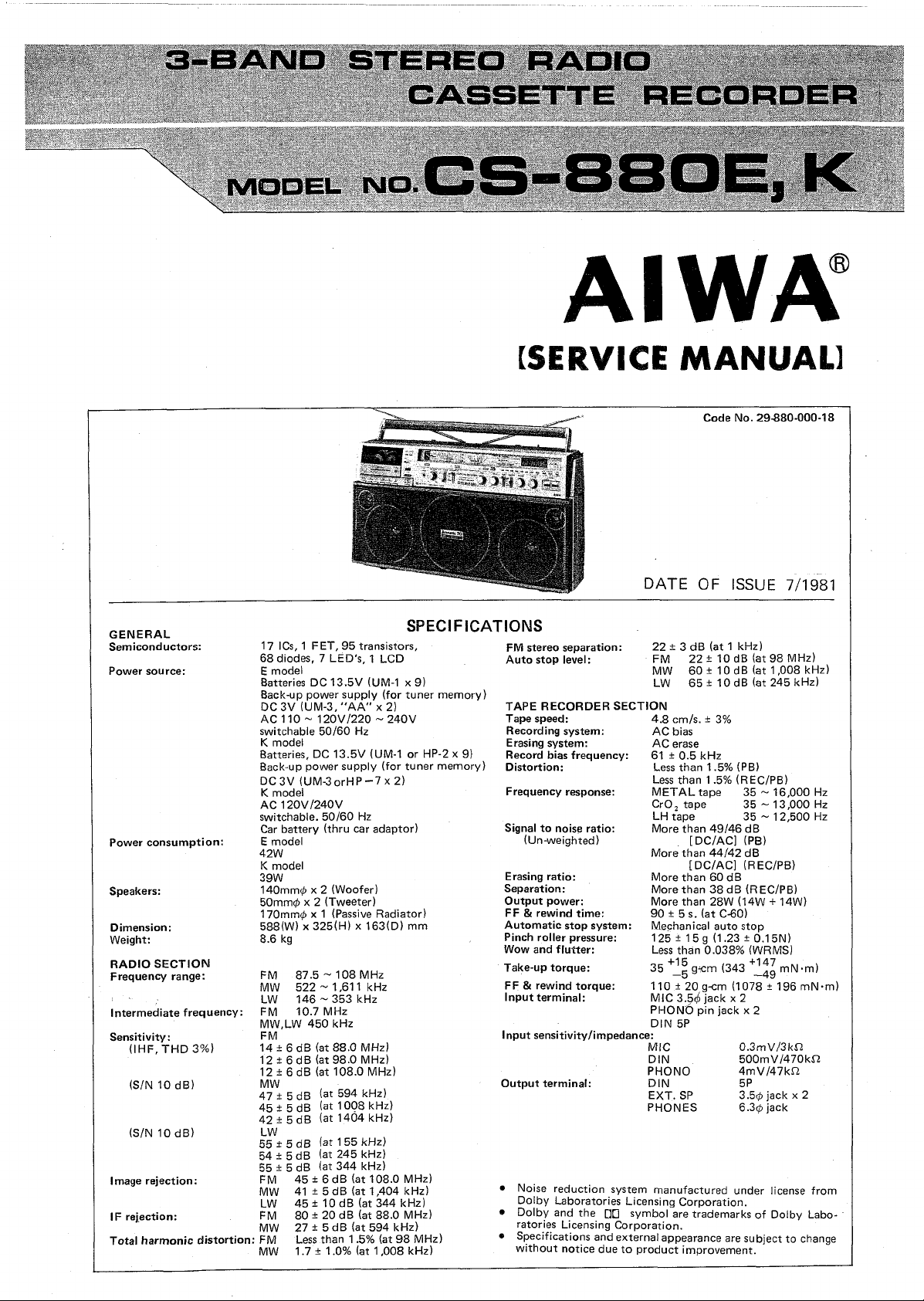
3-BAND STEREO R AD IO
CASSETTE RECOR DER
MODEL N O . C S b 8 Ü Ü E j K l
AIWA8
[SERVICE MANUAL]
Code No. 29-880-000-18
G E N ER A L
Semiconductors:
Power source:
Power consumption:
Speakers:
Dimension:
Weight:
RA D IO S EC T IO N
Frequency range:
Intermediate frequency:
Sensitivity:
(IH F, TH D 3% )
(S/N 10 dB )
(S/N 10 dB )
Image rejection:
IF rejection:
Total harmonic distortion
SPECIFICATIONS
17 10s, 1 F ET, 95 transistors,
68 diodes, 7 LED's, 1 LCD
E model
Batteries DC 13.5V (UM-1 x 9)
Back-up power supply (for tuner memory)
DC 3V (UM-3, " A A " x 2)
AC 110 ~ 120V/220 ~ 240V
switchable 50/60 Hz
K model
Batteries, DC 13.5V (UM-1 or HP-2 x 9)
Back-up power supply (for tuner memory)
DC 3V (U M - 3 orH P- 7 x2 )
K model
AC 120V/240V
switchable. 50/60 Hz
Car battery (thru car adaptor)
E model
42W
K model
39W
14Omm0 x 2 (Woofer)
5Omm0 x 2 (Tweeter)
17Omm0 x 1 (Passive Radiator)
588(W) x 325(H) x 163(D) mm
8.6 kg
87.5 ~ 108 MHz
FM
522 ~ 1,611 kHz
MW
146 ~ 353 kHz
LW
10.7 MHz
FM
LW 450 kHz
MW,
FM
6 dB (at 88.0 MHz)
14 ±
6 dB (at 98.0 MHz)
12 ±
6 dB (at 108.0 MHz)
12 ±
MW
5 dB (at 594 kHz)
47 ±
5 dB (at 1008 kHz)
45 ±
5 dB (at 14Ó4 kHz)
42 ±
LW
5 dB (at 155 kHz)
55 ±
5 dB (at 245 kHz)
54 ±
5 dB (at 344 kHz)
55 ±
45 ± 6 dB (at 108.0 MHz)
FM
41 ± 5 dB (at 1,404 kHz)
MW
45 ± 10 dB (at 344 kHz)
LW
80 ±20 dB (at 88.0 MHz)
FM
27 ± 5 d B (at 594 kHz)
MW
Less than 1.5% (at 98 MHz)
FM
1.7 ± 1.0% (at 1,008 kHz)
MW
DATE OF ISSUE 7/1 981
FM stereo separation:
Auto stop level:
TA PE R EC O RD E R SEC TIO N
Tape speed:
Recording system:
Erasing system:
Record bias frequency:
Distortion:
Frequency response:
Signal to noise ratio:
(Un-welghted)
Erasing ratio:
Separation:
Output power:
FF & rewind time:
Automatic stop system:
Pinch roller pressure:
Wow and flutter:
Take-up torque:
FF & rewind torque:
Input terminal:
Input sensitivity/impedance:
Output terminal: DIN
Noise reduction system manufactured under license from
Dolby Laboratories Licensing Corporation.
Dolby and the □□ symbol are trademarks of Dolby Labo
ratories Licensing Corporation.
Specifications and external appearance are subject to change
without notice due to product Improvement.
22 ± 3 dB (at 1 kHz)
FM 22 ± 10 dB (at 98 MHz)
MW 60 ± 10 dB (at 1,008 kHz)
LW 65 ± 10 dB (at 245 kHz)
4.8 cm/s. ± 3%
AC bias
AC erase
61 ± 0.5 kHz
Less than 1.5% (PB)
Less than 1.5% (REC /PB)
M E T A L tape 35 ~ 16,000 Hz
Cr0 2 tape 35 - 13,000 Hz
LH tape 35 - 12,500 Hz
More than 49/46 dB
[DC/AC] (PB)
More than 44/42 dB
[DC/AC] (REC /PB)
More than 60 dB
More than 38 d B (REC/PB)
More than 28W (14W + 14W)
90 ± 5 s. (at C-60)
Mechanical auto stop
125 + 15g (1.23 ± 0.15N)
Less than 0.038% (W RM S)
35 +^g g^cm (343 +^ g mN-m)
110 ± 20 g-cm (1078 ± 196 mN-ml
MIC 3.5^ jack x 2
PH ONO pin jack x 2
DIN 5P
MIC
DIN
PHO NO
EXT . SP
PHO N ES
0.3mV/3kfi
500mV/470kfi
4mV/47kf2
5P
3.50 jack x 2
6.30 jack
Page 2
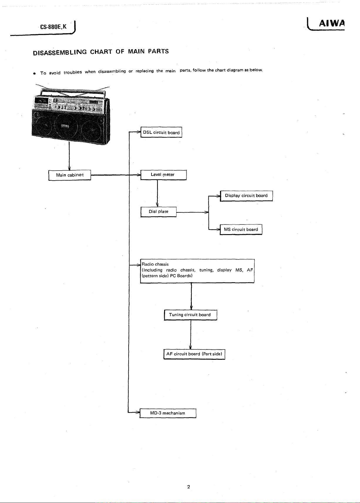
CS-880E,K j
DISASSEMBLING CHART OF MAIN PARTS
• T o avoid troubles when disassembling or replacing the main parts, follow the chart diagram as below.
DSL circuit board
L AIWA
^-|L__- -
---
Main cabinet
Level meter
54 Display circuit board
Dial plate
MS circuit board
MD-3 mechanism
2
Page 3
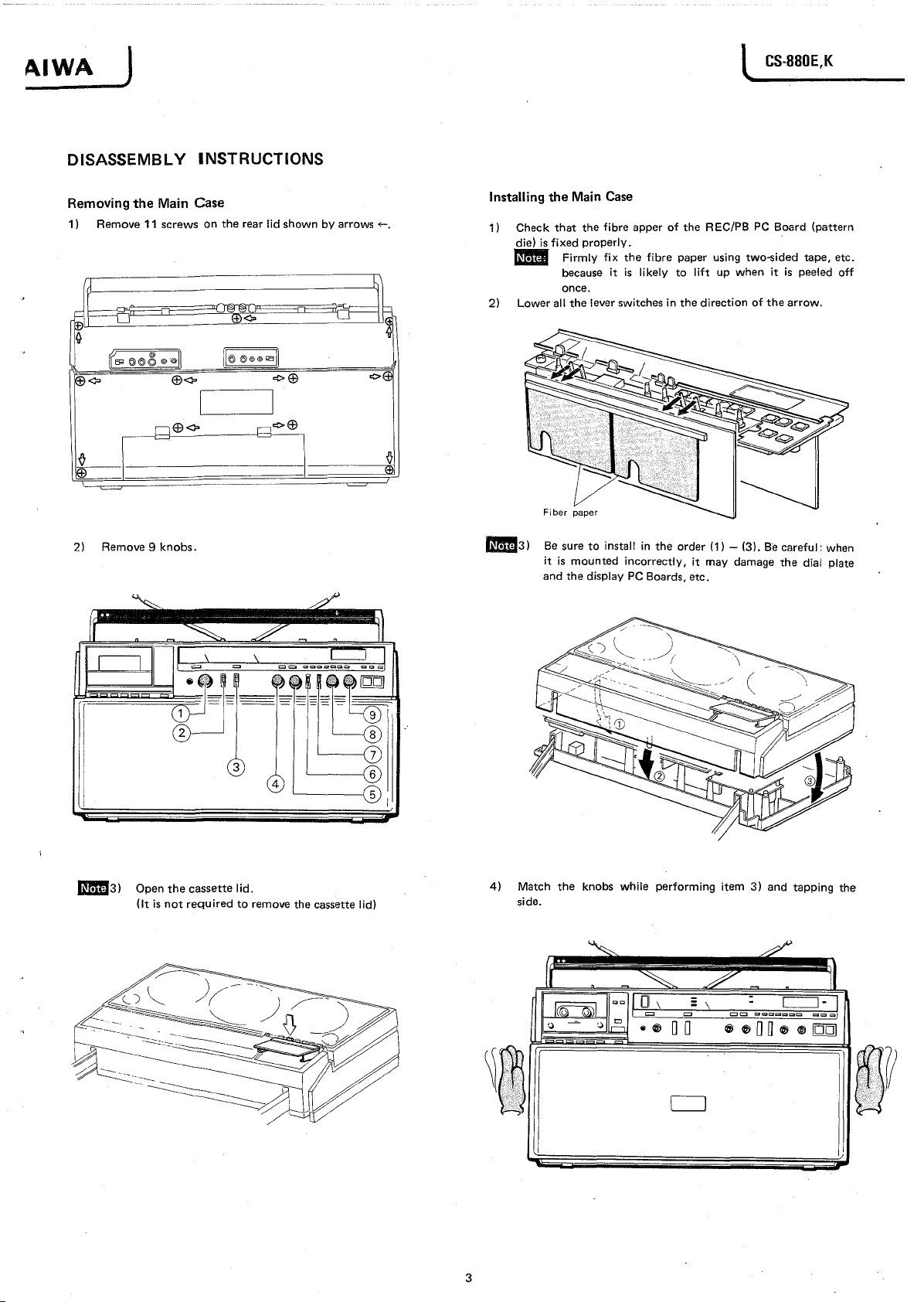
AIWA
J
DISASSEMBLY INSTRUCTIONS
CS-880E,K
Removing the Main Case
1) Remove 11 screws on the rear lid shown by arrows •
2) Remove 9 knobs.
Installing the Main Case
1) Check that the fibre apper of the RE C/PB PC Board (pattern
die) is fixed properly.
Q O I Firmly fix the fibre paper using two-sided tape, etc.
because it is likely to lift up when it is peeled off
once.
2) Lower all the lever switches in the direction of the arrow.
BB H 83) Be sure to install in the order (1) — (3). Be careful: when
it is mounted incorrectly, it may damage the dial plate
and the display PC Boards, etc.
E J ^ 3 ) Open the cassette lid.
(It is not required to remove the cassette lid)
4) Match the knobs while performing item 3) and tapping the
side.
3
Page 4
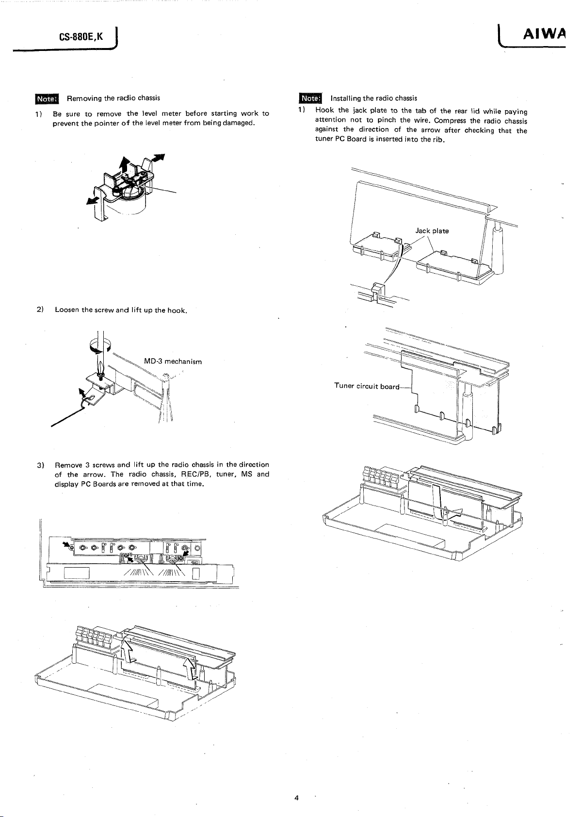
CS-880E,K
AIWÆ
IBBHI
1) Be sure to remove th e level meter before starting work to
2) Loosen the screw and lift up the hook.
Removing the radio chassis
prevent the pointer o f the level meter from being damaged.
Installing the radio chassis
1) Hook the jack plate to the tab of the rear lid while paying
attention not to pinch the wire. Compress the radio chassis
against the direction of the arrow after checking that the
tuner PC Board is inserted into the rib.
3) Remove 3 screws and lift up the radio chassis in the direction
of the arrow. The radio chassis, REC /PB, tuner, MS and
display PC Boards are removed at that time.
Page 5
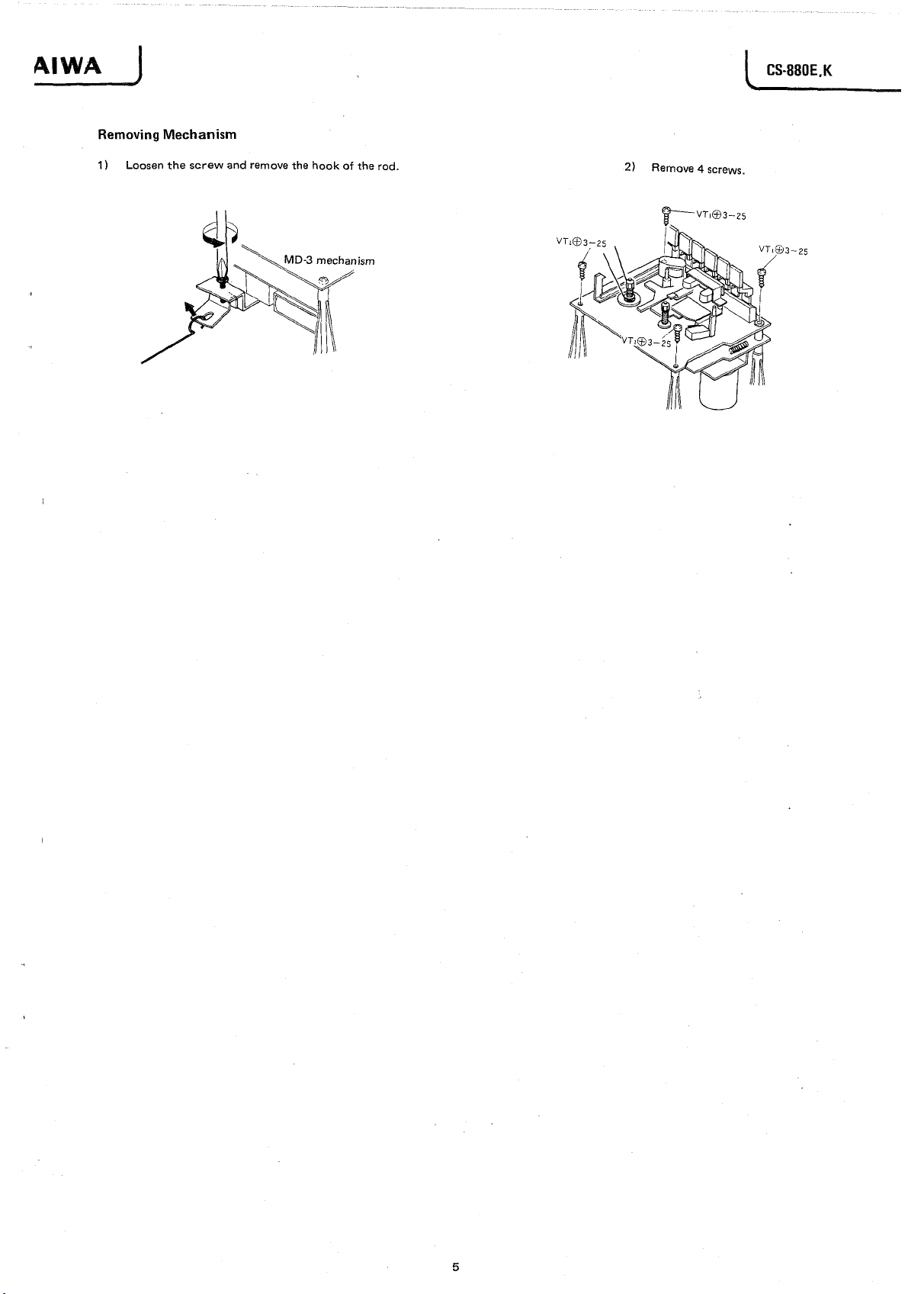
AIWA ]
Removing Mechanism
CS-880E.K
I
1) Loosen the sc rew and remove the hook of the rod.
2) Remove 4 screws.
5
Page 6
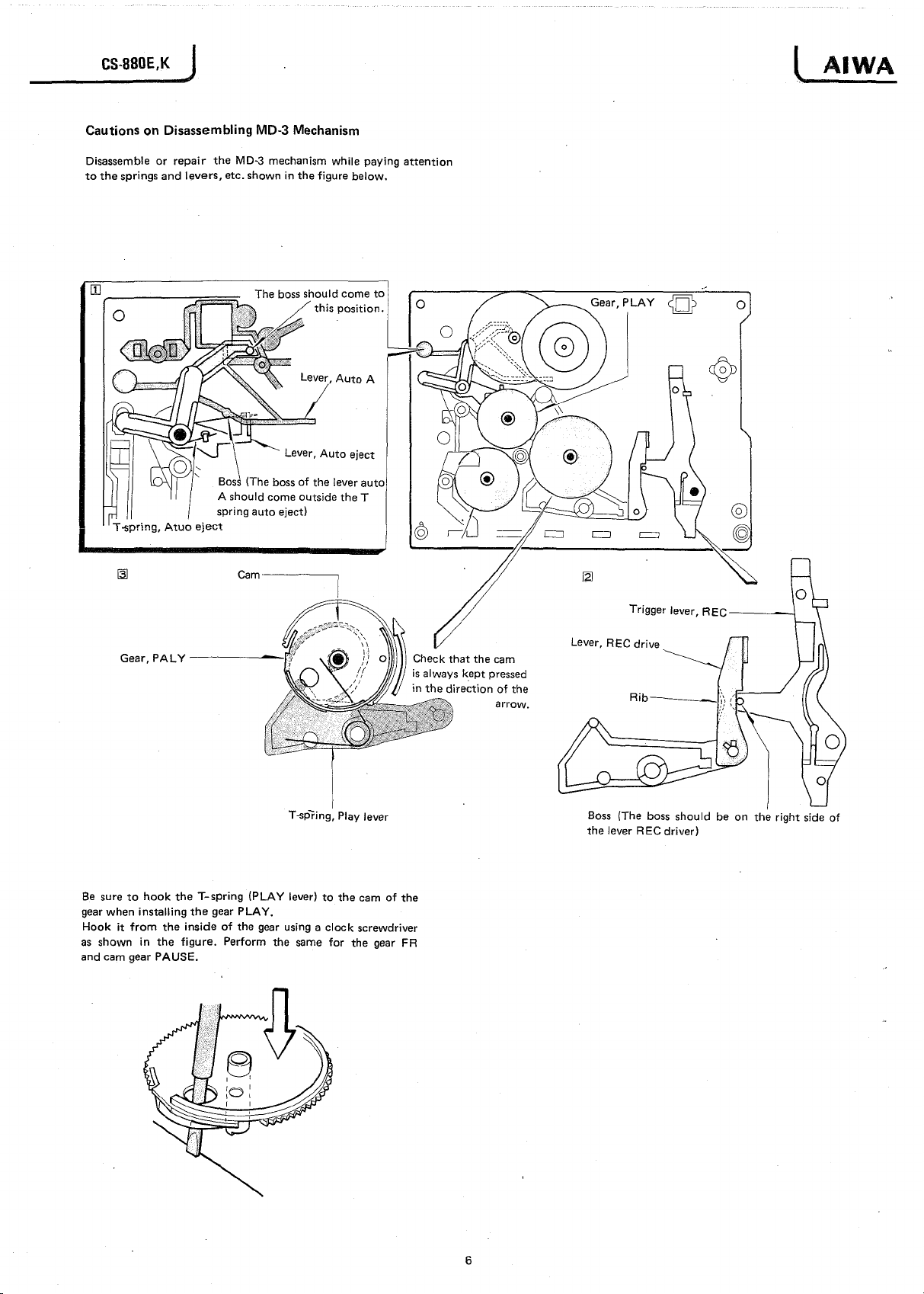
CS-880E.K
Cautions on Disassembling MD-3 Mechanism
Disassemble or repair the MD-3 mechanism while paying attention
to the springs and levers, etc. shown in the figure below.
[ AIW A
Be sure to hook the T-spring (PL A Y lever) to the cam of the
gear when installing the gear P LA Y.
Hook it from the inside of the gear using a clock screwdriver
as shown in the figure. Perform the same for the gear FR
and cam gear P AU S E.
the lever R E C driver)
6
Page 7
AIWA
J
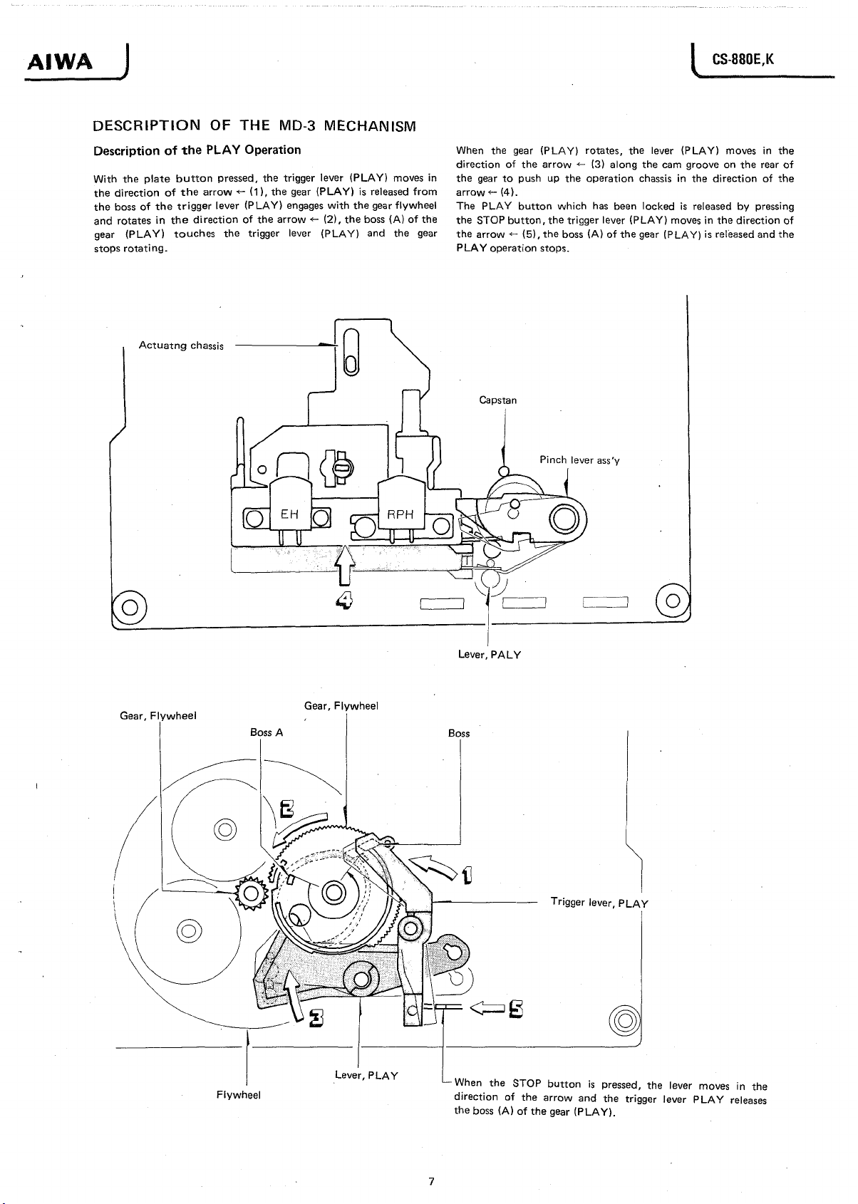
DESCRIPTION OF THE MD-3 MECHANISM
Description of the P LA Y Operation
With the plate b utton pressed, the trigger lever (P LA Y ) moves in
the direction of the arrow <- (1), the gear (P L A Y ) is released from
the boss of the trigger lever (PL A Y ) engages with the gear flywheel
and rotates in the direction of the arrow <- (2), the boss (A) of the
gear ( P LA Y ) touches the trigger lever (P LA Y ) and the gear
stops rotating.
CS-880E,K
When the gear (P LA Y ) rotates, the lever (PL A Y ) moves in the
direction of the arrow <- (3) along the cam groove on the rear of
the gear to push up the operation chassis in the direction of the
arrow «- (4).
The P L A Y button which has been locked is released by pressing
the STOP button, the trigger lever (PL A Y) moves in the direction of
the arrow *- (5), the boss (A ) of the gear (PL A Y) is released and the
PL A Y operation stops.
Gear, Flywheel
the boss (A) of the gear (PL A Y).
Page 8
CS-880E.K
- à . AIW A
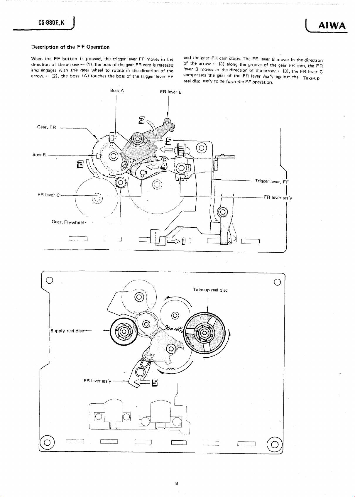
Description of the F F Operation
When the F F button is pressed, the trigger lever FF moves in the
direction of the arrow (1), the boss of the gear FR cam is released
and engages with the gear wheel to rotate in the direction of the
arrow. <- (2), the boss (A) touches the boss of the trigger lever FF
Boss A
FR lever B
and the gear F R cam stops. The F R lever B moves in the direction
of the arrow «- (3) along the groove of the gear FR cam, the F R
lever B moves in the direction of the arrow <- (3), the FR lever C
compresses the gear of the FR lever Ass'y against the Take-up
reel disc ass'y to perform the F F operation.
8
Page 9
AIWA
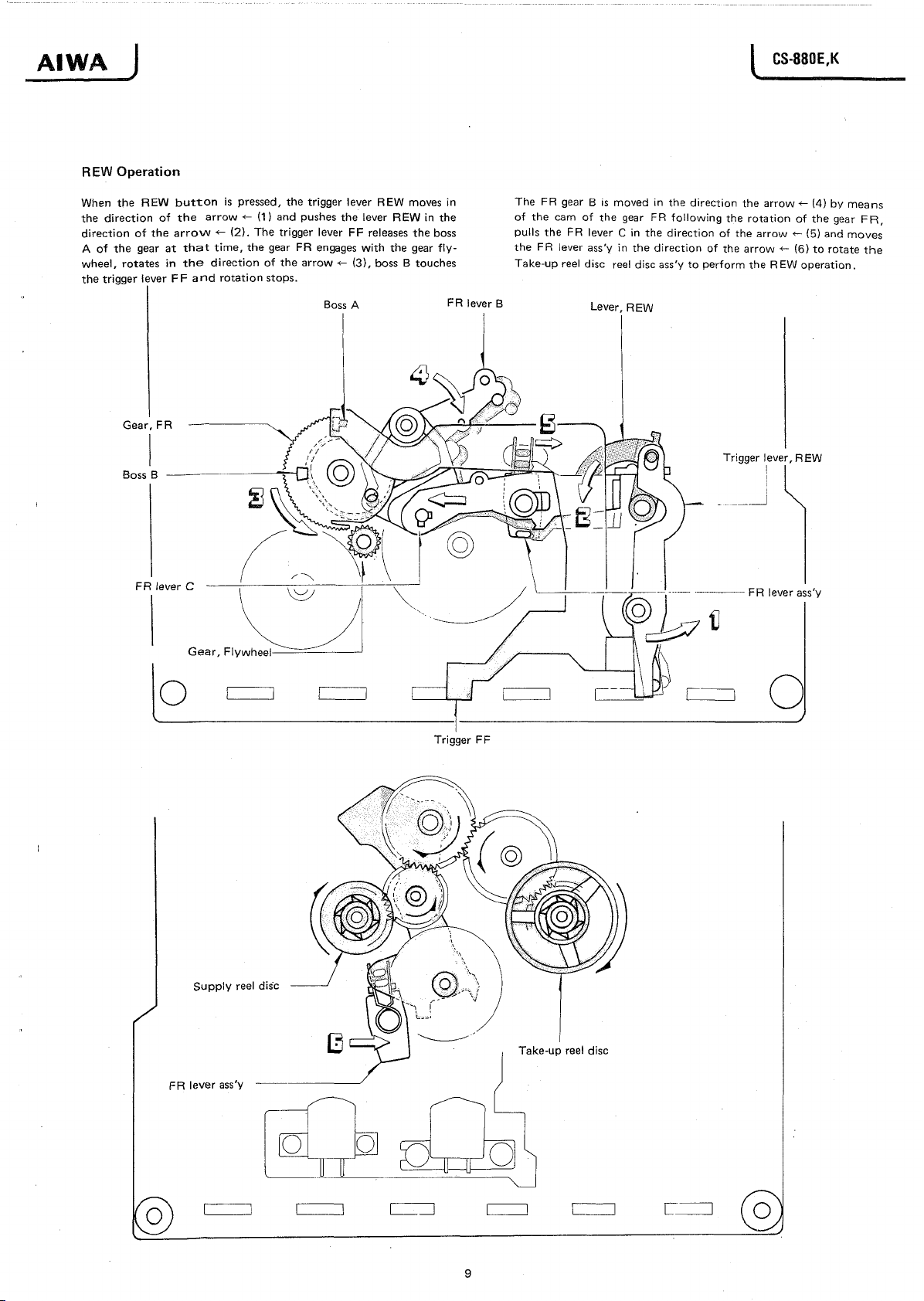
REW Operation
J [_
CS-880E,K
When the R EW bu tto n is pressed, the trigger lever R E W moves in
the direction of the arrow <- (1) and pushes the lever R E W in the
direction of the ar ro w <- (2). The trigger lever F F releases the boss
A of the gear at th a t time, the gear FR engages with the gear fly
wheel, rotates in th e direction of the arrow <- (3), boss B touches
the trigger lever F F a nd rotation stops.
The F R gear B is moved in the direction the arrow «- (4) by means
of the cam of the gear FR following the rotation of the gear FR ,
pulls the FR lever C in the direction of the arrow «- (5) and moves
the F R lever ass'y in the direction of the arrow <- (6) to rotate the
Take-up reel disc reel disc ass'y to perform the R EW operation.
9
Page 10
CS-880E.K
J [ AIW A
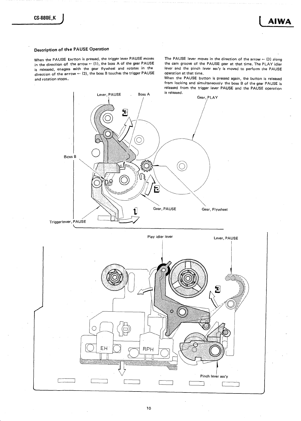
Description of th e PAU SE Operation
When the P A U S E button is pressed, the trigger lever P A U SE moves
in the direction o f the arrow *- (1), the boss A of the gear P A U SE
is released, enages with the gear flywheel and rotates in the
direction of the ar row <- (2), the boss B touches the trigger P A USE
and rotation stops.
The PA U S E lever moves in the direction of the arrow •*- (3) along
the cam groove of the PA U SE gear at that time. The P LA Y idler
lever and the pinch lever ass'y is moved to perform the P A US E
operation at that time.
When the PA U SE button is pressed again, the button is released
from locking and simultaneously the boss B of the gear PA U SE is
released from the trigger lever P AU S E and the P A US E operation
10
Page 11
AIW A
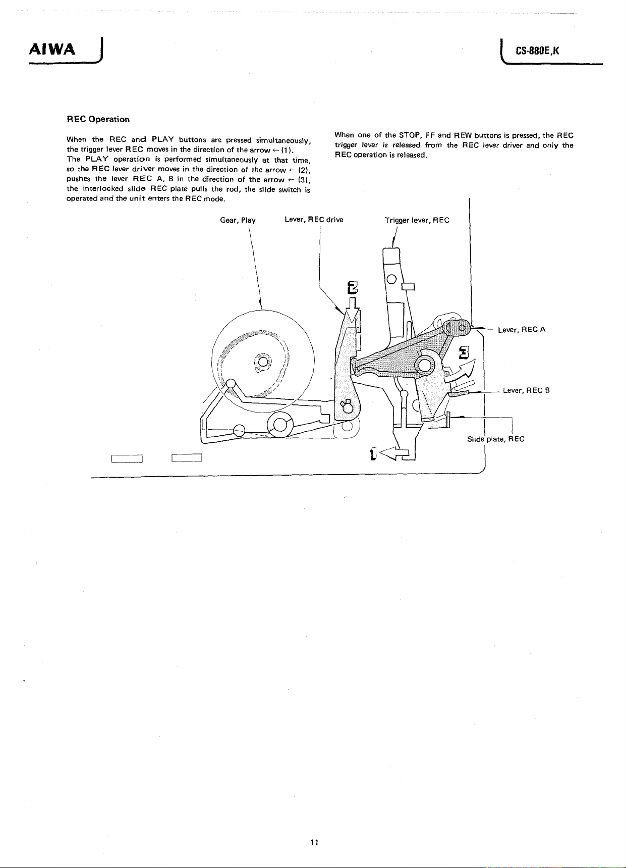
REC Operation
When the R E C a nd PL A Y buttons are pressed simultaneously,
the trigger lever R E C moves in the direction of the arrow +- (1 ).
The P L A Y operation is performed simultaneously at that time,
so the R EC lever d river moves in the direction of the arrow «- (2),
pushes the lever R E C A, B in the direction of the arrow <- (3),
the interlocked slide R E C plate pulls the rod, the slide switch is
operated and the un it enters the R EC mode.
J
CS-880E.K
When one of the ST OP , F F and RE W buttons is pressed, the R EC
trigger lever is released from the R EC lever driver and only the
RE C operation is released.
Gear, Play Lever, RE C drive Trigger lever, RE C
11
Page 12
CS-83QE.K
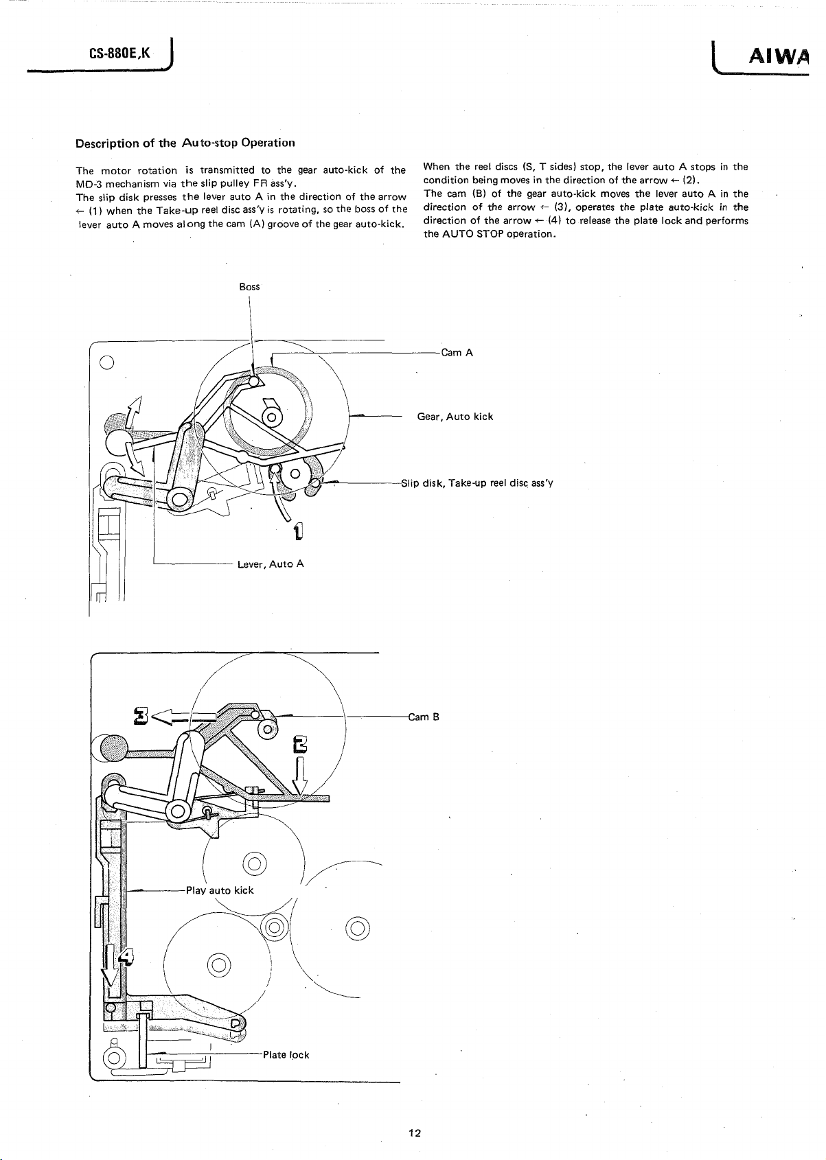
Description of the Auto-stop Operation
The motor rotation is transmitted to the gear auto-kick of the
MD-3 mechanism via the slip pulley F R ass'y.
The slip disk presses th e lever auto A in the direction of the arrow
<- (1) when the Take-up reel disc ass'y is rotating, so the boss of the
lever auto A moves along the cam (A) groove of the gear auto-kick.
Boss
When the reel discs (S, T sides) stop, the lever auto A stops in the
condition being moves in the direction of the arrow (2).
The cam (B) of the gear auto-kick moves the lever auto A in the
direction of the arrow «- (3), operates the plate auto-kick in the
direction of the arrow «- (4) to release the plate lock and performs
the A UTO STO P operation.
Cam A
Gear, Auto kick
ip disk, Take-up reel disc ass'y
12
Page 13

AIWA j
SPRING APPLICATION POSITION
CS-880E.K
13
Page 14

CS-880E,K
1 AIW A
14
Page 15

AIWA J
MECHANICAL PARTS
Ref. No.
1-1
1-2
1-3
1-5
1-6
1-7
1-8
1-9
1-10
1-11
1-1 2
1-13 09-017-851-01 Back cover ass'y
1-1 4
1-15
1-16
1-1 7
1-18
1-1 9
1-20
1-21
1-22
1-23
1-24
1-25
1-26
1-27
1-28
1-29
1-30a
1-30b
1-31a
1-31b
PARTS LIST
Part No.
09-01 7-850-01
82 -5 8 7 - 0 0 1-0 1
82 -5 8 7 - 2 3 4-0 1
82 -58 7 - 0 0 7 -0 1
82 -5 8 7 - 0 3 6-0 1
82 - 5 8 7 -0 0 9 -01
82 -58 7 - 0 1 0 -0 1
82 - 5 8 7 -0 2 8 -0 1
82 - 5 6 3 -0 3 2 -01
82 -58 7 - 0 0 3 -0 1
82 - 5 8 7 -2 2 1 -0 1
82 - 5 8 7 -2 3 9 -01
87 - 3 2 1 -0 9 7 -2 1
Part No.
Changed to
Main case ass'y
Cabinet, Main
Damper A, Rubber
Panching * 1
Badge
Side panel R
Side panel L
Panel, Front
Cassette plate
Window, Dial
E-spring (tact)
P-spring, Tact A
Q T j + 3 - 1 2
82-587-635-01 Drone cone ass'y
82-587-227-01
82-576-241-01
82-587-020-01
82-587-021-01
P-spring, Earth
E-spring, Earth
Tact push-key
Push-button
82-587-218-01 T-spring, Cassette lid
82-587-202-01 Cassette box
82-587-004-01
82-587-011-01
87-081-979-01
82-587-219-01
82 - 5 8 7 -0 3 8 - 0 1
82 - 5 8 7 -21 3-0 1
82 - 5 8 7 -21 4 -01 C-spring, Terminal B
82 - 5 8 7 -21 6-0 1 C-spring, Terminal C
82 - 5 8 7 -21 5 -01 Term inal plate U t
82 - 5 8 7 -21 7 -01 Terminal plate U 3
82 - 5 8 7 -22 6 -01
82 - 2 7 7 -38 2-0 1 Spring, Terminal
81 - 2 3 5 -21 1 -01
87-3 4 9 -0 95 -2 1
Window, Cassette
Decorative panel. Cassette
Decorative screw 3-12
P-spring, Cassette holder
Back cover ass'y
C-spring, Terminal A
Sheet, Faiber
Term inal plate D
U T , +3 -8 1
82-534-203-01 Click plate spring R
82-587-21201
82-587-231-01
82-587-233-01
Shaft, Handle
Rubber bushing 6x 1 0
Rubber bushing 7 x 10
87-038-039-01 Wire binder
82-587-208-01
Rubber bushing 3 x 5
82-587-013-01 Handle L
82-587-014-01 Handle grip
82-587-012-01 Handle R
82-587-005-01 Battery room lid
82-587-237-01
M cushion 14 x 35 x 5
82-587-247-01 M cushion 7 x 281 x 7
82-587-017-01
Knob
82-563-014-01 Knob, T O G GL E
82-587-023-01
Knob, VO LU M E -(UP)
82-587-024-01 Knpb, V O LU M E (DOWN)
82-587-030-01 Name plate. Spec. (E model only)
82-587-03101
Name plate. Spec. (K model only)
82-587-025-01 A C jack plate (E model only)
82-587-041-01
AC jack_plate (K model only)
Description
^ CS-880E.K
* mark in this part list shows exclusive part.
Common
Model
*
*
•
*
*
*
CS-990
* 1
*
*
*
*
*
CS-350
*
*
*
*
*
*
*
*
*
*
*
*
*
*
*
*
*
*
*
*
*
*
*
*
*
*
CS-990 4
*
*
*
*
*
*
Q'ty
1
1
18
1
1
1
1
1
1
1
1
1
1
13
1
1
1
1
1
1
1
1
1
1
1
1
1
1
1
1
1
1
1
1
1
1
2
4
1
1
1
1
1
1
15
Page 16

CS-880E.K
EXPLODED VIEW —2
B
,K
1 I 2
[ AIWA
D
H
16
Page 17

AIWA
J
CS-880E,K
Ref. No.
2-1
2-2
2-3
2-4
2-5
2-6
2-7
2-8
2-9
2-10
2-11
2-12
2-13
2-14
2-15 82-588-634-01
2-16 82-587-008-01
2-17
2-18
2-19
2-20
2-21
2-22
2-23
2-24
2-25
2-26
2-27
2-28
2-29
2-30 87-063-113-01
2-31
2-32 82-587-254-01
Part No.
87-043-058-01
87-033-166-01
82-587-220-01
82-587-205-01
82-588-209-01
82-587-242-01
82-587-211-01
82-587-225-01
82-587-206-01 Rod 87.8
82-587-608-01
82-587-238-01
82-587-201-01
82-587-207-01
82-162-037-01 Push-button B 2
87-064-084-01 Holder, ECM 30
82-587-019-01 Push-key, RE C mute
82-563-24701 E-spring, Air-damp
87-096-045-01 String, Dial
87-078-003-01 Air-damp unit ass'y
82-587-240-01 LED reflector
82-587-224-01 Holder, Switch
87-040-143-01 Counter
82-587-209-01 Rubber belt
82-587-203-01 Holder, Counter
82-587-037-01 Push-key, RE C
82-587-018-01 Push-key, Tape recorder
82-588-208-01
82-587-049-01
Part No.
Changed to
Description
Whip antenna 2
Antenna terminal 2
Terminal plate, Antenna
Rod, RE C
Cushion 1 5 x 15 x 4 1 CS-770 1
Sheet, Fiber A
Cushion, Battery
Rod 37.8
Shield, Front
Rubber cushion 10 x 25 x 14 1
Chassis
Holder, Dial plate
Earth, R EC
Dial plate (Silver)
Common
Model
*
*
*
*
*
AD-R500
CS-770
*
*
CS-990 1
*
*
*
Q'ty
*
#
*
Rubber cushion 33-6-3
Cushion WA
Push-button, DS L
Rod 38.3
CS-770 1
*
*
2
1
1
1
1
1
1
1
1
1
1
1
1
1
1
1
1
1
1
1
17
Page 18

CS-880E
EXPLODED VIEW -3
B
.kJ
1 I 2
PW I.7-3.5-0.25
[ AIWA
U02-I2
U© 2-I2
PWI. 7-3.5-0.25
PW I.7-3.5-0.25
H
18
Page 19

AIW A J
[ CS-880E,K
Ref. No.
3-1
3-2
3-3
3-4
3-5
3-6
3-7
3-8
3-9
3-10
3-11
3-12
3-13
3-14
3-15
3-16
3-17
3-18
3-19
3-20
3-21
3-22
3-23
3-24
3-25
3-26
3-27
3-28
3-29
3-30
3-31
3-32
3-33
3-34
3-35 87-038-056-01
Part No.
82-585-325-01
82-585-277-01
82-585-337-01
82-585-279-01
82-585-255-01 REC blocking lever
82-585-319-01
82-585-254-01 Slide plate, Eject
82-585-311-01
82-585-290-01 C-spring, Back tension
82-585-215-01 Supply reel platform ass'y
82-585-292-01 C-spring, Slip disk
82-585-272-01
82-585-210-01 Take-up reel platform ass'y
82-585-294-01 T-spring, Center shift
82-585-312-01
82-585-253-01 Lever, Brake R
82-585-286-01
82-585-252-01
82-585-265-01 R E V lever
82-585-231-01 F R lever ass'y
82-585-235-01
82-585-223-01 Play Idler lever ass'y
82-585-313-01 F-spring, Play idler
82-585-364-01
82-585-296-01 T-spring, Pinch lever
82-585-340-01 Plate lock ass'y
82-585-338-01 Rubber cushion. Play lever
82-585-295-01 T-spring, Actuating
82-585-208-01
82-585-209-01 Head base
82-585-291-01 C-spring, RPH
82-588-628-01 Shield plate
87-073-005-01
82-585-284-01 P-spring, Actuating
Part No.
Changed to
Description
Outsert chassis
Plate button, FR
Plate button, REC
Lever A, Eject
P-spring, Cassette pressure
E-spring, Lid lock
Slip disk T
E-spring, Brake R
Rubber cushion, Brake
Lever, Brake L
Gear A, RE W
Pinch lever B ass'y
Actuating chassis
Steel ball 20
Wire binder
Common
Model
CS-770
Q'ty
1
3
3
1
1
1
1
1
1
1
1
1
1
1
1
1
1
1
1
1
1
1
1
1
1
1
1
1
1
1
1
1
1
1
19
Page 20

CS-880E,K
L A IW A
20
Page 21

AIW A
J
CS-880E.K
Ref. No.
4-1
4-2
4-3
4-4
4-5
4-6
4-7
4-8
4-9
4-10
4-11
4-12
4-13
4-14 82-585-271-01
4-15
4-16
4-17
4-18
4-19
4-20
4-21
4-22
4-23
4-24
4-25
4-26
4-27
4-28
4-29
4-30
4-31
4-32
4-33
4-34
4-35
4-36
4-37
4-38
4-39
4-40
4-41
4-42
4-43
4-44 82-585-301-01
4-45
4-46
4-47
4-48
4-49
4-50
4-51
4-52
4-53
4-54
4-55
4-56
4-57
4-58
4-59
4-60
4-61
4-62
4-63 87-087-029-01
4-64 87-081-483-01
4-65
4-66
Part No.
82-585-289-01
82-585-285-01
82-585-317-01
82-585-306-01
82-585-283-01
82-585-282-01
82-585-327-01
82-585-268-01
82-585-269-01
82-585-270-01
82-585-248-01
82-585-264-01
82-585-297-01
82-585-299-01
82-585-262-01
82-585-263-01
82-585-298-01
82-585-261-01
82-585-260-01
82-585-303-01
82-585-308-01
82-585-341-01
82-585-300-01
82-585-217-01
82-585-216-01
82-585-244-01
82-585-245-01
82-585-256-01
82-585-304-01
82-585-246-01
82-585-247-01
82-585-249-01
82-585-250-01
82-585-307-01
82-585-266-01
82-585-267-01
82-585-314-01
82-585-258-01
82-585-259-01
82-585-308-01
82-585-331-01
82-585-257-01
82-585-321-01
82-585-203-01
82-585-315-01
82-585-332-01
82-585-229-01
82-585-243-01
82-585-324-01
82-585-336-01
82-585-287-01
82-585-323-01
82-585-281-01
82-585-242-01
82-585-326-01
82-588-206-01
87-038-039-01 Wire binder 1
82-587-241-01 E-spring, Slide plate
82-587-228-01 Slide plate RE C ass'y
82-585-335-01
82-585-342-01
82-587-232-01
Part No.
Changed to
Description
Shaft lock 1
C-spring lock
E-spring, Button lock
T-spring, Play lever
Slide plate, FR auto
Slide plate. Motor switch
Slide plate key ass'y 1
Auto A lever 1
Auto B lever 1
Plate auto kick
Lever, PAU SE
FR lever D
T-spring, FR lever A
Auto eject lever 1
T-spring, Auto eject
FR lever B
F R lever C
T-spring, FR lever B
Trigger lever, REC 1
Lever, RE W
T-spring, Trigger (RE C) 1
E-spring, R EW lever
E-spring, F R lever
T-spring, FR cam
Slip pulley F R ass'y
Drive gear
Play cam gear
F R cam gear
Trigger lever, PA US E
T-spring, Trigger (PA U SE)
Gear, P AU SE
Gear, Auto kick
PL A Y lever
Lever, R EC drive
T-spring, RE C lever
REC A lever
REC B lever
E-spring, R EC
Trigger lever, P LA Y
Trigger lever, RE W 1
T-spring, R EW lever
C-spring, RE W lever
FF trigger lever
E-spring, Trigger P LA Y
T-spring, Auto kick 1
Mechanism chassis B ass'y 1
E-spring, Slide plate 1
E-spring, R EC lock 1
Flywheel ass'y 1
Gear, Flywheel 1
C-spring, Flywheel 1
Rubber belt FR B 1
Rubber belt. Flywheel
Holder, Pause switch 1
Holder, Motor 1
Motor pulley
Thrust bearing B
Rubber cushion, R EC lever CS-770
T-spring, Plate lock
Rubber cushion
Motor screw, M2.6
Rubber cushion, P AU SE lock
Holder, R EC switch
Common
Model
*
*
*
Q'ty
1
1
1
1
1
1.
1
1
1
1
1
1
1
1
1
1
1
1
1
1
1
1
1
1
1
1
1
1
1
1
1
i
1
1
1
1
1
1
1
1
1
1
1
1
1
21
Page 22

CS-880E,K
J
Description of Circuitry
1. Block Diagram o f Synthesizer Tuner
[ AIW/3
ROD ANTENNA
EXT. Q t t
ANTENNA
TERMINALS O -
D2q
a
to AUDIO
Fig. 1
2. Outline of PL L Frequency Synthesizer
The P LL (phase-locked loop) requency synthesizer is a cirucit
which uses the extrem ely stable frequency of a crystal oscillator
as the reference signal to produce the frequencies desired. For
instance, to pick up a station broadcasting on a frequency of
100 M Hz , a local oscillation frequency (f0 : output frequency of
voltage-controlled oscillator) supplied to the mixer of 110.7 MHz
(100 + 10.7) is required. This particular unit adopts a prescaler
which employs a pulse swallow system to divide the frequency,
and send it to the programmable counter inside the controller
IC. The output frequency fn then enters the phase comparator.
The frequency of the extremely stable 4.5 MHz crystal oscillator
is counted down (1/180) at the same time and the reference
frequency fref of 25 kHz is sent to the phase comparator. The
phases of f n and f ref are compared and the difference between
the two is detected. If there is no difference, the loop is locked;
if there is a difference, the control voltage passes through the
low-pass filter, it is fed out to the VCO and the VCO is con
trolled until fn is made equivalent to 25 kHz.
The reference frequency fref for AM reception is 9 kHz (or 10
kHz). The VCO frequency signal is sent directly to the pro
grammable counter.
C R Y S T A L
OS C ILL A T O R 4.5M HZ
V. C.O iV O LT A GE CO NTROL LE D OS CILLA TO R
Fig. 2
2-1. Operation During FIVI Reception
The pulse swallow system is first outlined.
The relationship between fosc and fref is expressed as:
fosc = ^ x ^ r e f
If N is assumed to be P notation:
fosc = (n, + pn2 + P2 n3 + .........+ Pn~ ‘ nn) fref
= P (nt IP + n2 + Pn3 + . . . . + P n~ 2 nn) fref
If, now,the part including the second digit and above is made Np:
fosc = p <ni/p + Np) fref
This is modulated to become:
fosc = K + PNp + Pn, - P n ^ fr e f
= [(Np — n ,) P + n, (P + 1)] fref
The above represents the principle of the pulse swallow system.
In order to achieve the relationship expressed in formula (2) by
physical means, this unit has a prescaler with two frequency
division ratios, 1/16 and 1/17. In formula (1), this corresponds to
P = 16. Actual operation is as follows: when the signal produced
by dividing fosc by (P + 1) is counted down n, times at the first
programmable divider digit and nt becomes 0, the P-divided
signal is counted down (Np — nt ) times equivalent to the number
of the first digit subtracted from the number of the second and
higher digits of the programmable divider, and the cycle ends.
This cycle is performed with f ref equal to 25 kHz.
When fs = 100 MHz is received:
f|F is 10.7 MHz and so therefore fosc = 100 + 10.7 = 110.7 MHz
From formula (1): IM = ^ = 4428
If this figure is re-expressed in the sexadecimal notation, and
made to correspond with 114C formula (2):
Np= 114, n, =C
Therefore, fref x [(114 — C )x 1 0 + C x 11] = f0sc
If this is re-expressed in the decimal notation:
25 kHz x [(162 + 161 + 4 - 12) x 16 + 12 x 17] = 110.7 MHz
What happens is that the prescaler divides the frequency by 1/17
for the first 12 counts and then by 1/16 until 264 counts, and
this switching operation is repeated. The swallow counter is
locked at 12 and the programmable counter is locked at 264.
...............................
ZO Nhz
' ................................ (1)
.......................
(2)
22
Page 23

AI WA
J
CS-880E,«
I
2-2. O peration During A M Reception
When fs = 594 kHz is received:
fs = 594 kH z and f|p = 450 kHz
Therefore: fosc = 594 + 450 = 1044 kHz
Since f ref = 9 kHz (or 10 kHz), (at LW fref = 1 kHz)
4.5 MHz-i-9 kHz = 500
fosc (1 044 kHz) -i- 9 kHz = 116
Therefore, the crystal oscillator frequency division is locked at
500 and th at o f the programmable counter at 116.
3. Description o f ICs Used
Fig. 3 is a bloc k diagram of the ICs in the P L L frequency synthe
sizer section an d LC D indicator section.
(AM or F M ) ' C * !C2 IC3
3-1. Prescaler /iPB553A C
This IC is energized during FM reception, it selects either the
1/16 or 1/17 frequency division ratio in accordance with the
command fro m the swallow counter inside the codntroller, and
it sends the signal to the controller's programmable divider.
3-1-1. Pin Configuration
Fig. 3
3-2. Controller fiPD1703C-515
Contained in this 1C are the conventional programmable divider
section and control section.
3-2-1. Pin Configuration
Pin no.
1, 2
3 CE
4
5,6
7
8
9-13
14
15-21
22-25
26
27
28 AM
Name
E01 , E02
PSC
X I, X2
SD
MU TE
D Î-D 5
V d d
Sa~Sg
K0- K3
FM
GND
Function
Charge pump output pins of phase detector;
since signals are fed out during AM/FM re
ception, one or other is connected to LPF .
High: Normal operation
Low: Memory held, operation stops
Feeds out frequency division ratio switch
ing signal to prescaler.
Crystal oscillator pins
High: Auto tuning stop mode
Low: Auto tuning enable mode
Feeds out high level signal during key
operation. (Usedformutingofsignal system)
Display digit signal output pins
Only D1 and D2 are used with this unit and
are connected to LC D driver.
Power supply pin
Key matrix key return signal source pins
Key matrix key return signal input pins
Input pin for FM prescaler output
Ground
AM fosc input pin
Fig. 5
Pin no.
1
2
3
4
5
6
7
8
Name
<
o
IN
CH K
GND
OU T
PSC
NC
NC
Function
Power supply
o
VC O input pin
Check pin, connected to GN D at all times
Ground
Output pin
Frequency division ratio setting pin (frequency
division setting input from controller)
Not used
Not used
Fig. 4
3-2-2. Key Matrix Functions
K o (2 5 ) K I (2 4 1 K 2 (23) K3 (22)
S2 0 f t
So ( 2 I ) ----
Sb (2 0 )
Sc (IQ )
Sd ( I S )
Se (17 )
Sf ( 16 ) ---------
■>=—
S2 3 ¿ V
----
*=—
--------
--------
--------
*5
(D OWN) S2 I
(M 4 I S 24 ^
.......
V
(U P ) S 2 2 (M EMORY)
(M 3) S2 5
S 3 1 > V
(L W ) ^
STA/o YN. y r
* 6
s27
* 2
• V
(M 2) S26 ^
(M 6 ) S 28
(F M ) S30 jf*
S! 3
AUTO /MANU AL
,r, * V
(M l)
’(M 5)
(MW)
IFo
Fig. 6
23
Page 24

CS-880E,K
J [ AIWA
• The function in parentheses is displayed by key operation based
on a momentary switch (marked 00 ).
• Manual/auto selection (*1)
Manual/auto sele ction is performed by a fixed switch but in this
unit the key op erations are carried out with momentary switches
which, thanks to th e flip-flop circuit, have the same functions as
fixed switches.
When connected: A u to tuning
When disconnected : Manual tuning
• LCD static/dynamic selection (*2)
This determines w hether the LC D display system should be
static or dynam ic. In this unit, static specifications apply and so
the diode is sho rte d.
• IF frequency selection (*3, *4)
Alignment is made with the FM IF frequency by IF t and IF 0
shorting and open combinations. The IF frequencies used by this
unit are 10.675 M H z, 10.700 MHz and 10.725 MHz and so the
combinations appear as follows:
IF offset frequency
10.675 MHz (blue)
10.700 MHz (red)
10.725 MHz (orange) Shorted
Color of ceramic filter indicated in parentheses.
• Japan/US use selection (*5)
When connected: U S specifications
When disconnected.: Japan specifications
® AM frequency interval selection ("6)
The AM channel frequency intervals are selected to 10 kHz or
9 kHz.
When connected: 10 kHz
When disconnected: 9 kHz
3-3. LC D driver (MSM 5829G S)
Indication is provided on the LCD by connecting the three
serial output data from the controller (juPD1703C-515)
IF i
Open
Open
IFo
Shorted
Open
Shorted
Fig. 7
Pin no. Name Function
8,9, 10,4
5,7 ,6 ,
56, 1,2,5 2
53, 55, 54
31,32 , 33, 27
28, 30, 29
47, 48, 50, 43
44, 46, 45
12, 13
11,3,5 1,
42, 34,
41
15
16 OSC
17
18 S E R IA L IN Data indicated with shift regis
19 CLO CK
20
21,49
22
23 SE L EC T This function is not used and so
24
25 RE S ET
26
14
35, 36, 37
38, 39, 40
SEG M EN T O U T
A1, B1, C1, D1
E l, F1, G1
A2, B2, C2, D2
E2, F2, G2
A5, B5, C5, D5
E5, F5, G5
AA , BA , CA, DA
EA, F A, G A
F l, F2
DP1, DP2, DP3,
DP4, DP5
CH
VS S
SE R IA L O UT Not used
LO AD
V DD
BI/ RBO Not used
RB I
COM
COM
LC D segment output pins
(see Fig. 8*)
Ground Pin
LC D A C drive frequency pin;
with this unit, the circuit is con
figured as below.
ter data input pins are fed into
this pin in synchronization with
clock pulses. (Connected to pin
19 of controller IC)
Sync, input pin when data is fed
into, or fed out of shift register.
(Connected to pin 9 of control
ler IC)
Input pin for latching shift
register contents.
High: Shift register contents are
transmitted to decoder.
Low: Final contents at high
level are held (Connect
ed to pin 10 of controller
IC)
Power supply pin
pin is always at high level or, in
other words, it is connected to
V DD-
Pin for determining whether or
not leftmost display digit is to
indicate a numeral or not. In
this unit, it displays only signifi
cant figures and so it is used at
the low level, or in other words,
it is connected to Vg s (ground).
Pin for switching display to
segment or dot; since segment is
used in this unit, it is set to high
level or, in other words, it is
connected to V q d -
This pin feeds out an output
with the reverse phase to that of
COM. In this unit, it is not used
for direct display but for AM
and FM +B selection as men
tioned later.
This pin feeds out a signal with
the reverse phase to that of out
put and 7 segments for AC
drive of the LCD; it drives the
LCD common pin.
Not used
24
LCD DISPLAY
Fig . 8
Page 25

AIWA
j
I CS-880E.K
4. Other Circuits
4-1. FM /A M +B Po w er Selector Circuit
I C 2 T C 4 0 II8 P
to RAD IO
Switching is performed with a 4-NAND gate IC (IC2).
4-2. Scan Auto Stop Circuit
4-2-1. Operation During FM Reception
The S-curve output pin 10 and meter output pin 15 of IF IC
(IC2, HA12413) are used. If pin 10 has a voltage where V(B)
< V(10) < V (A ) with respect to the preset point A and point
B voltages (about +0.5 V with respect to pin 10 voltage during
tuning), no output appears at point (C) and when there is an
output at pin 15, point (F) Is set to a low level and no signal
is fed out to point (C). A trigger pulse is produced at point (G)
by the above two AN D circuits, this is applied to the SD pin
of the controller IC and the scanning is stopped.
4-2-2. Operation During AM Reception
The IF output from pin 12 is smoothed and point (F) is reduced
to the low level by the output. As with FM reception, a trigger
pulse is produced at point (G) and the scanning stops. [IC3
(N JM4558D) does not work during AM reception.]
TE RMINAL
NAME
FM
<DP4>
AM
<DP3>
COM
Q20 8ASE
at FM
"LTL
_n_r
“LTL
__
H IG M LEVEL
at AM
JIT
TTL
U L
_
LOW LEVEL
[U
Fig. 10
When the FM band selector key Is depressed, pulses with the
same phase are fed out to IC3 (MSG5829G) DP4 and COM.
As this output passes through the NA ND gate IC (TC4011BP),
a high level output is produced at N AND gate 1 output and this
causes Q20 to turn ON. As a result, Q19 turns ON and the FM
+B is obtained. With AM reception, no output appears at DP4,
the N AN D gate 1 output is set to the low level and with Q20
O FF , Q18 turns ON and the AM +B is obtained.
5. Dynamic Super Loudness (DSL) Circuit
If the DS L circuit is compared with the loudness circuit, it is
seen that both function to boost the low-range (bass) and high-
range (treble) frequencies with respect to the midrange fre
quencies but there are the following major differences.
5-1. Characteristics
OUTPUT
FREQUENCY
Fig. 12
The loudness system functions to boost the midrange frequencies
too. However, the D SL system keeps this increase down to the
bare minimum.
With the loudness system, the characteristics do not change with
the strength of the signal entering the volume control for provid
ing a tape in the control [normally scale unit 5 (center posi
tion)] , and the volume control's tap position is mechanical,
25
Page 26

CS-880E,K
J
AlWys
L
meaning that the characteristics change. A t a scale position lower
than the volume control's tap position, the loudness characteris
tics are provided regardless of the strength of the sound level
and, in contrast, even when the sound level is low, the effect is
impaired by the con tro l's scale position.
However, the D S L system judges the strength of the sound
level by electrical means and features a configuration which
produces dynamic super loudness characteristics.
5-2. DSL Circuit Configuration
The D S L circuit comprises the equalizer circuit which produces
the D SL characteristics, the detector circuit which judges the
strength of the sound level and the control circuit which sup
presses the DS L characteristics when the sound is high.
MA IN AM R CIR C U IT
EM IT T E R
FO L LO W E R
VO LUM E LE V EL
CONPEN SA TION
Fig. 13
5-2-1. Equalizer C ircuit
An ordiany direct-coupled amplifier feedback circuit (T-type
bridge circuit) is provided with time constants, and its character
istics generated.
Tow T-ty>pe bridge circuits are connected in series and the time
constants are divided into the left side for bass [R 361, 359,
C359, 361 ] and right side for treble.
The characteristics of each of the twin filters connected to pins 3
and 8 of IC351 (TA7137P) are attenuated by frequency f,
determined by constants R 1, R2 and C 1.
Q--^ —VW———J—-o
INPUT Cl I c 2 OUTPUT
^R2
o
------i-------
o
OUTPUT
f I
2 7rJC iC2 R i F?2
FR EQUENCY
5-2-2. Detector Circuit
The level of this circuit is set by the frequency division ratio of
two resistors.
5-2-3. Control Circuit
This circuit is the same as an AL C circuit used for normal record
ing although it diffères in that its attack time and recovery time
are extremely short.
Because of the boosted level, the output must be not distorted.
When a signal exceeding a certain fixed level is fed out, it is
taken out by the Q49 emitter, the IC7 AL C circuit functions and
the input of pin 2 is controlled.
+ B ] C 7
Fig. 16
The DSL circuit with the above-mentioned configuration is
mixed with a main amplifier. The ICI (AN7146) input has a
differential amplifier configuration, and when a flat signal enters
transistor Q1 at one side of the differential amplifier from the
volume control, a flat signal also enters the DSL circuit simul
taneously. Q2 is basically a negative feedback pin but when the
output (signal with D SL characteristics) of the D SL circuit is fed
into the Q2 input, differential operation is provided by Q1 and
Q2.
The DS L block input transistor Q47 is used to invert the phase.
As a result, the phase is inverted at the DSL block input and
output sides and so the differential operation of Q1 and Q2
becomes a mixing operation. Meanwhile, the feedback from the
output inside IC7 does not change and negative feedback opera
tion results.
When the signal level is low in Fig. 13, there is a high degree of
mixing by Q1 and Q2 inside IC I so that the D SL feeds out a
strong signal, and the bass nad treble are greatly boosted. H ow
ever, when the signal level is high, the DS L block output is
suppressed, the amount of mixing by Q1 and Q2 inside IC1 is
reduced, and since the Q2 input is reduced to a fraction,almost
all of it becomes the signal fed in from Q1.
The resistor inserted across the ground and O FF side pin of the
DSL ON /OFF switch functions to compensate for the difference
in the volume when the switch is selected.
Fig. 14
Fig. 15
26
Page 27

AIW A
j
ACC ESSO RI ES/PAC KAGE
Ref. N o.
1
2
3
4
5
6a
6b
7
8
9
10
11
12 82-916-740-01
13a
13b 87-034-871-01
Part No.
82-587-855-01
82-587-852-21
82-587-853-21
87-051-137-11
87-056-626-01
82-587-908-01
82-587-909-01
82-587-907-01
87-051 -171-11
87-056-00941
87-056-008-11
87-056-016-01
87-034-883-01
Part No.
Changed to
Description
Printed indiv., Packing
Cushion L, Printed indiv.
Cushion R , Printed indiv.
Poly-vinyl sack
Poly-vinyl sack
Instructions booklet (E model only)
Instructions bookelt (K model only)
Sticker, POP
Poly-vinyl sack (for instruction)
Distributors list
Label, A C power cord (K model only)
Tag, Main voltage (K model only)
Tape cassette, DMC-164
AC power cord (E model only)
AC power cord (K model only)
Common
Model
*
*
*
*
*
*
CS-88QE.K
Q'ty
1
1
1
1
1
1
1
1
1
1
1
1
1
1
1
Page 28

810725(1 )-Z
A I W A c o . , l t d .
Printed in Japan
Page 29

AIW A
J
ELECTRICAL MAIN PARTS LIST
Symbol No.
Part No.
Description
ST U M ER Cl R C U IT B O ARD SEC TION >
PCB-A 82-587-611-21 Tuner circuit board
CP1
($>IC1
IC2
IC3
IC4 V 87-027-430-11
Q1 89-319-233-01
Q2 89-303-803-01
Q3,4,5,7,
8,9,10,11,
13,14,15,16,
18,20,21,22
25,26,27
Q6,23,24
Q12,19 89-110-154-01
Q17
D1,2
D3,4,5,6, 87-027-097-01 Diode, 1S1555
7,8,9,11
D10
L1,10,11,13
L2
L3,4
L5
L6
L7,8 87-005-126-01 Coil, Im ri
L9
L12
TC1
TC2 87-011-109-01
CF1,2
CF3 87-008-225-01 AM ceramic filter
IFT1 87-008-226-01
IFT2 87-008-223-01 AM IFT
SFR1 87-021-566-01
SFR2
PIN-1 87-049-045-01
R50
C108
C19
C48
C105
^R E C /PB Cl
PCB-B
ICI ,2
IC3,4
IC5,9
IC10
Q1,2
03,4,5,6,
7,8,17,
18,19,20,
21,22,27,
28,29,30,
31,32,33,
34,35,36,
37,38,42,
44
82-587-626-11 FM front end
87-027-752-01
87-027-734-01
87-027-235-01 IC, NJM4558D
89-318-154-01
89-318-156-01
89-403-135-01
87-027-753-01
87-027-431-01 Zener diode, RD6.2EB2
87-003-051-01 Choke coil, 470juH
87-005-121-01 FM coil
82-587-680-01
82-755-607-01 MW OSC coil
82-587-681-01
87-008-227-01 FM coil
87-003-045-01 Choke coil, 22juH
87-011-108-01 Trimmer, 8pF
87-008-245-01
87-021-567-01
87-025-317-01
87-014-040-41
87-014-048-41 430pF PP
87-014-057-41
87-014-065-01 2200pF PP
RC U IT BO AR I
82-587-658-01
87-027-540-01
87-027-754-01
87-027-539-01
87-027-656-01
89-322-405-01
89-318-154-01
1C, 553AC
IC, HA12413
IC, LA3361
Transisotr, 2SC1923 (O)
Transistor, 2SC380 (O)
Transistor, 2SC1815 (Y )
Transistor, 2SC1815 (BL)
Transistor, 2SA1015 (Y)
Transistor, 2SD313 (E)
Diode, KV1236Z
MW/LW bar antenna coil
LW OSC coil
Trimmer, 15pF
Ceramic filter kid
AM IFT
Semi-fixed resistor, 5k£2-B
Semi-fixed resistor, 10k£2-B
Pin, 12P
< Resistor >
^7 iZ V z \n Nonflammable
< Capacitors >
200pF PP
1000pF PP
D SECT ION >
REC/PB circuit board
IC, AN7146
IC, LM1111C
1C, LA3161
IC, TC4066BP
Transistor, 2SC2240 GR )
Transistor, 2SC1815 (Y)
resistor
Symbol No.
Q39,40
041 89-318-464-01 Transistor, 2SC1846 (R)
Q43
Q45,46 89-320-011 -21
D1,2,7,8, 87-027-097-01 Diode, 1S1555
9,10,11,12,
13,17,18,19,
352
D3,4,5,6
D14
D16 87-027-199-01 Zener diode, 05Z-15U
L1,2
L3,4
L7,9,13,14,17
L8
L1 1,1 2
L I 5,16
CP1
LPF1
J 1,2,3,4,6
J5/ S34 87-049-059-01 DIN jack w/switch (DIN)
J7,8 82-587-632-01
J9
VR1
VR2,3 87-021-668-01
VR4
VR5
S1
S2
S3
S4
S5
S6
S7,8,15
S3 2
SFR 1 ,2
SFR3,7,8
SFR4
SFR5,6 82-587-634-01
R83,84
R245
R164
Z L r 202
A R153,154,
220,246
ZÎ\R162,163
C49,50,89,
90
C17,18
C13,14,75,
76
C115,116
C107,108,
117,118
Part No.
89-318-155-01 Transistor, 2SC1815 (GR )
89-322-364-01 Transistor, 2SC2236 (Y)
88-052-188-11
87-027-346-01 Zener diode, H Z11A2L
87-008-173-01
82-487-654-01 Coil, 10mH
87-003-039-01 Choke coil, 36juH
82-491-661-01 Choke coil, 600juH
87-003-051-01 Choke coil, 470juH
87-005-088-01
82-587-641-11 Bias OSC unit
87-030-070-01 Low-pass filter
82-587-633-01
87-049-043-01 Jack, 6.30 (PH ONES)
87-021-671-01 Volume, 50ki2-A
87-021-669-01 Volume, 100ki2-W (BA LA N C E)
87-021-667-01 Volume, 20ki2-A (VO L UM E )
87-031-655-01
82-588-622-21
87-031-631-01 Lever switch (TA PE SEL EC TO R )
87-031-620-01 Lever switch (R EC OR D)
82-563-609-01 Slide switch (PHO NO/A UX)
87-031 -622-01
87-031-619-01
82-431-604-01
87-021-564-01
87-021-624-01 Semi-fixed resistor, 50kf2-B
87-021-514-01 Semi-fixed resistor, 200kH-B
82-588-634-01
87-025-209-01
87-025-313-01
87-025-320-01
87-029-108-01
87-029-089-01
87-029-090-01
87-029-365-01
87-014-053-01
87-014-055-01
87-015-311-01
87-015-367-01
87-015-312-01
Transistor, 2SC2001 (K ,L)
Diode, 1S188 (FM)
Trap coil, 10mH
Coil, 5.6mH
Jack plate ass'y (PHONO,
MIC-L,R, P L A Y E R SYNC )
Jack plate ass'y
(E X T SP-L,R)
(R EC V O LU M E)
Volume, 50kf2-A
(BA SS, T R E B L E)
Lever switch (FUN CTIO N)
Slide switch (REC/PB)
Lever switch (MOD E)
Push-swtich (DO LBY-NR ,
POW E R, D SL)
Slide switch (OSC)
Semi-fixed resistor, 1 ki2-B
Semi-fixed resistor, 100H-B
Earth terminal
< Resistors >
3.3ki2 Metal film resistor
4.7 n Nonflammable
100i2 2w Nonflammable
1i2 1/4w Fuse resistor
4.7£2 Fuse resistor
22£2 !4w Fuse resistor
22i2 1/4w Fuse resistor
< Capacitors >
680pF PP
820pF PP
O.ljitF 10V Aluminum solid
0.1 5mF 10V Aluminum solid
0.22/jlF 10V Aluminum solid
Description
resistor
resistor
Page 30

Symbol No. Part No.
Description
Symbol No.
Part No.
Description
Symbol Nc
C77,78
< CONTROL
PCB-C
®IC1
®IC 2,4
®IC 3
Q1,2,3,4
05
D1,2,3,4,
5,6,7,11,
12,13,14,15,
16,17,18,19,
20,21,22,23,
24,25,26
D27,29
D28
D30
X1
S19,20,21,
22,23,24,
25,26,27,
28,29,30,
31
PL1,2
PCB-D
®IC 6
0401,402,403,
404.405.411,
412,413,414,
415,416
0406
0407,409
0408
D401
D402
D403
D404,405,
406,407,
408,409,
410.411,
415
D412,413,
414
D416
S17,18
SFR4 01 ,402
C412
C407
PCB-E
IC7,8
047,48,49,
50,51,52,
73,74
D351
L10
PIN 4
PIN-2
87-015-313-01 0.33juF
10V Aluminum solid
CIR C U IT BO A RD SECTIO N >
82-587-604-11
87-027-750-01
87-027-564-01
87-027-751-01
89-318-154-01
89-500-303-01
87-027-097-01
87-027-716-01
87-027-758-01
82-587-603-01
87-030-083-01
87-031-498-01
82-587-605-01
82-587-606-01
82-587-615-21
87-027-713-01
89-327-854-01
89-111 ■
154-51
89-313-
834-01
89-106-
834-51
87-027-
756-01
87-027-
365-01
87-027-
332-01
87-027-
097-01
87-027-716-01
87-027-228-01
87-031-496-01
87-021-624-01
87-015-318-01
87-015-425-01
82-587-617-21
87-027-176-01
89-318-154-01
87-027-097-01
82-587-610-01
87-049-038-01
82-481-647-01
Control circuit board
IC, /¿PD1703C514
IC, TC4011BP
IC, MSM 5829GS
Transistor, 2SC1815 (Y)
FET , 2SK30 (O)
Diode, 1S1555
LE D, GL-PPR22
(AU TO OP ER AT E/ FM ST E RE O )
LED, GL-9PG22 (DO LBY- NR)
LCD (F RE Q U E N C Y IN DIC AT OR )
Crystal resonator
Push-switch (TU N IN G , DOW N, UP,
M EM O RY , 1,2,3,4,5,6, FM, MW,
LW )
Pilot lamp
Electric conduction rubber
MS circuit board
IC, TC9138P
Transistor, 2SC2785 (E)
Transistor, 2SA1115 (E,F)
Transistor, 2SC1383 (S)
Transistor, 2SA683 (RS)
LED, SL-1160L (M S P RO G RA M )
Diode, S5277B
Zener diode, HZ6B1 L
Diode, 1S1555
LED, GL-9PR22 (PE A K 0, +3, +7)
Zener diode, 05Z-7.5U
Tact switch (PR O GR AM , R E SE T )
Semi-fixed resistor, 50k£2-B
< Capacitors >
0.1juF 10V Aluminum solid
1juF 25V Aluminum solid
DSL circuit board
IC, TA-7137P Stereo type
Transistor, 2SC1815 (Y)
Diode, 1S1555
Coil, DC-DC
Pin, 3P
Pin, 4P
PIN-3
87-049-034-01
Pin, 4P
< Capacitors >
C361,362
C359,360
87-015-311-01
87-015-313-01
0.1juF 10V Aluminum solid
0.33juF 10V Aluminum solid
REC AM P CIR C U IT B O A RD SECTION >
PCB-F
Q23,24,25,
26
L5,6
SF R 9 1 0
C81,82
<4 MONITO R C IR U C IT B O A R D SECTION >
PCB-G
Q9,10
Q11,12,13,
14,15,16
PIN
82-588-617-11
89-318-154-01
87-005-088-01
87-021-672-01
87-015-311-01
82-588-633-21
89-322-405-01
89-318-154-01
87-032-634-01
RE C amp circuit board
Transistor, 2SC1815 (Y)
Micro inductor, 5.6mH
Semi-fixed resistor, 50k£2-B
< Capacitor >
0.1m F 10V Aluminum solid
Monitor circuit board
Transistor* 2SC2240 (GR)
Transistor,, 2SC1815 (Y)
Pin, 4P
< REC MU TE CIR C U IT B O A R D SECTIO N >
PCB-H
Q72
D1
S9
PCB-I
D1
82-587-618-21
89-110-154-01
87-027-097-01
82-587-642-01
82-587-619-21
87-027-731-01
RE C mute circuit board
Transistor- 2SA1015 (Y)
Diode, 1 SI 555
Push-switch (R EC M UTE)
LED circuit board
LED , SR-535D (RE CO RD )
^ LIGHT SWITCH C IR C U IT B OAR D SECTION >
PCB-J
S33
A p c b -k
D501
J10,11
ZLS16
A f i
A f 2
A
R501
82-587-648-21
86-992-604-01
82-551-672-21
87-027-609-01
87-032-958-01
87-031466-01
87-035-192-01
87-098-022-01
87-035-219-01
87-098-013-01
87-033-147-01
87-025-194-01
Light switch circuit board
Push-switch (LIG HT )
Power circuit board
Encapsulated diode
AC-DC jack
Slide switch
(V O LT A G E S ELE C TO R )
Fuse, " T " 4A
Fuse lable, " T " 4A
Fuse, " T ” 500mA
Fuse label, " T " 500mA
Fuse clamp
< Resistor >
220Í2 2w Metal film resistor
< M ISC ELL ANEO U S >
A t i
A t i
RPH
EH
SOL1
SP1,2
SP3,4
SP5
LM 1,2
ECM1,2
M1
S10,14
S11
82-587-651-01
82-587-652-01
87-046-159-01
87:046-189-01
82-585-601-21
82-587-644-11
82-563-602-01
82-587-635-11
82-588-642-01
87-041-015-01
87-045-135-01
87-031-548-01
87-031-537-01
Power transformer
(E model only)
Power transformer
(K model only)
REC/PB head
Erase head
Solenoid
Speaker (Woofer)
Speaker (Tweeter)
Passive radiator ass'y
Level meter
ECM , ESM-10PB
Motor DC EG
Leaf switch (M OTOR, S YN C RA TE )
Micro switch (P LA Y)
512
513
CO N4
CON-3
CON-2
CON-1
C1,2
A\ Safety <
This symbol
the safety of
safety specif
this symbol,
C MOS IC ha
The C-MOS
by static ele»
ing articles.
1. Need to I
and to b
deposit.
2. To use s
consumpi
second.
3. Do not p
the circui
4. The ICs
MOS IC s
Page 31

Symbol No.
Part IMo.
Description
Symbol No.
Part No.
Description
Q39,40
Q41
Q43
Q45,46
D1,2,7,8,
9,10,11,12,
13,17,18,19
352
D3,4,5,6
D14
D16
L I ,2
L3,4
L7,9,13,14,17
L8
L11,12
L1 5,16
CP1
LPF1
J1 ,2,3,4,6
J5 , S 34
J7,8
J9
VR1
VR2,3
VR4
VR5
51
52
53
54
55
56
S7,8,15
S3 2
SF R 1 ,2
SFR3,7,8
SFR 4
SF R 5,6
R83,84
R245
R164
i^ R 202
R153,154,
220,246
Î\R162,163
R172
C49,50,89,
90
C17,18
C13,14,75,
76
C115,116
0107,108,
117,118
89-318-155-01
89-318-464-01
89-322-364-01
89-320-011-21
87-027-097-01
88-052-
-188-11
87-027-
-346-01
87-027-
-199-01
-173-01
87-008-
82-487-
-654-01
87-003-
-039-01
661-01
82-491 -
87-003-
051-01
-088-01
87-005-
-641-11
82-587-
-070-01
87-030
82-587-
633-01
87-049-059-01
82-587-632-01
87-049-043-01
87-021-671-01
87-021-668-01
87-021-669-01
87-021-667-01
87-031-655-01
82-588-622-21
87-031-631-01
87-031-620-01
82-563-609-01
87-031-622-01
87-031-619-01
82431-604-01
87-021-564-01
87-021-624-01
87-021-514-01
82-587-634-01
82-588-634-01
87-025-209-01
87-025-313-01
87-025-320-01
87-029-108-01
87-029-089-01
87-029-090-01
87-029-365-01
87-014-053-01
87-014-055-01
87-015-311-01
87-015-367-01
87-015-312-01
Transistor, 2SC1815 (G R)
Transistor, 2SC1846 (R)
Transistor, 2SC2236 (Y )
Transistor, 2SC2001 (K ,L)
Diode, 1S1555
Diode, 1S188 (FM)
Zener diode, H Z11A2L
Zener diode, 05Z-15U
Trap coii, 1 umH
Coil, 10mH
Choke coil, 36juH
Choke coil, 600juH
Choke coil, 470;uH
Coil, 5.6mH
Bias OSC unit
Low-pass filter
Jack plate ass'y (PHO NO,
MIC-L,R, P L A Y E R SYNC )
DIN jack w/switch (DIN )
Jac k plate ass'y
(E X T SP-L,R)
Jack , 6.30 (PH ON ES)
Volume, 50ki2-A
(RE C V O LU M E )
Volume, 50kf2-A
(B AS S, T R E B L E )
Volume, 100ki2-W (BA LA N CE )
Volume, 20kH-A (V O LU M E)
Lever switch (FUN CT IO N )
Slide switch (REC/PB)
Lever switch (TA PE SEL EC TO R)
Lever switch (REC O RD )
Slide switch (PHON O/AU X)
Lever switch (M ODE)
Push-swtich (DO LBY-NR,
PO W ER , DSL )
Slide switch (OSC)
Semi-fixed resistor, 1 ki2-B
Semi-fixed resistor, 50ki2-B
Semi-fixed resistor, 200ki2-B
Semi-fixed resistor, 100i2-B
Earth terminal
< Resistors >
3.3ki2
4.7Í2
10OÍ2 2w
4.7S2
22n
22n
Metal film resistor
Nonflammable
resistor
Nonflammable
resistor
V z \ N
Fuse resistor
Fuse resistor
%w Fuse resistor
1Aw Fuse resistor
< Capacitors >
680pF PP
820pF
0.1¡xF
0.1 5mF
0.22mF
PP
10V
Aluminum solid
10V Aluminum solid
10V Aluminum solid
C77,78 87-015-313-01
CONT RO L C IRC U IT BO/
PCB-C
(3&IC1
($) IC2,4
®IC 3
01,2,3,4 89-318-154-01
05
D 1,2,3,4,
5,6,7,11,
12,13,14,15,
16,17,18,19,
20,21,22,23,
24,25,26
D27,29 87-027-716-01 LED , GL-PPR22
D28
D30 82-587-603-01 LCD (F R EQ U E N C Y IND ICA TO R)
X1 87-030-083-01 Crystal resonator
S19,20,21, 87-031498-01
22,23,24, M EM OR Y, 1,2,3,4,5,6, FM , MW,
25,26,27, LW)
28,29,30,
31
PL1 ,2 82-587-605-01
PCB-D
®IC 6
0401,402,403,
404.405.411,
412,413,414,
415,416
0406
0407,409
0408
D401
D402
D403
0404,405,
406,407,
408,409,
410.411,
415
D412,413,
414
D416
S17,18
SFR4 01,402
82-587-604-11 Control circuit board
87-027-750-01 IC, mPD1703C514
87-027-564-01 IC, TC4011BP
87-027-751-01 IC, MSM5829GS
89-500-303-01 FE T, 2SK30 (O)
87-027-097-01 Diode, 1S1555
87-027-758-01 LED, GL-9PG22 (D OLB Y-NR )
82-587=606=01
82-587-615-21
87-027-713-01
89-327-854-01
89-111
154-51
89-313-
834-01
89-106-
-834-51
87-027-
756-01
87-027-
365-01
87-027-
332-01
87-027-
097-01
87-027-716-01
87-027-228-01
87-031496-01
87-021-624-01
0.33juF 10V Aluminum solid
^RD SECT IO N >
Transistor, 2SC1815 (Y )
(AUT O O PE RA T E/FM ST ER EO )
Push-switch (TU NIN G, DOWN, UP,
Pilot lamp
Electric conduction rubber
MS circuit board
IC, TC9138P
Transistor, 2SC2785 (E)
Transistor, 2SA1115 (E ,F )
Transistor, 2SC1383 (S)
Transistor, 2SA683 (R S)
LED, SL-1160L (M S PRO G RA M )
Diode, S5277B
Zener diode, HZ6B1 L
Diode, 1S1555
LED, GL-9PR22 (PE A K 0, +3, +7)
Zener diode, 05Z-7.5U
Tact switch (PRO G RA M , R E SE T )
Semi-fixed resistor, 50ki2-B
< Capacitors >
C412
C407
PCB-E
IC7,8
047,48,49,
50,51,52,
73,74
D351
L10
PIN-4
PIN-2
87-015-318-01
87-015425-01
82-587-617-21
87-027-176-01
89-318-154-01
87-027-097-01
82-587-610-01
87-049-038-01
82481-647-01
0.1/uF 10V Aluminum solid
1/liF 25V Aluminum solid
DSL circuit board
IC, TA-7137P Stereo type
Transistor, 2SC1815 (Y )
Diode, 1S1555
Coil, DC-DC
Pin, 3P
Pin, 4P
Page 32

I CS-880E,K
Symbol No.
PIN-3
Part No.
87-049-034-01
Pin, 4P
Description
< Capacitors >
C361,362
C359,360
87-015-311-01
87-015-313-01
0.1juF 10V
0.33juF 10V
Aluminum solid
Aluminum solid
< REC AMP CIR CUIT BOAR D SECTION >
PCB-F
023,24,25,
26
L5,6
SFR9,10
€81,82
82-588-617-11
89-318-154-01
87-005-088-01
87-021-672-01
87-015-311-01
RE C amp circuit board
Transistor, 2SC1815 (Y)
Micro inductor, 5.6mH
Semi-fixed resistor, 50ki2-B
< Capacitor >
0.1juF 10V
Aluminum solid
< MO NITOR C IRUCIT BOAR D SECTION >
PCB-G
Q9,10
Q11,12,13,
14,15,16
PIN
82-588-633-21
89-322-405-01
89-318-154-01
87-032-634-01
Monitor circuit board
Transistor, 2SC2240 (GR)
Transistor, 2SC1815 (Y )
Pin, 4P
< REC MUTE CIR CUIT B O ARD SECTIO N >
PCB-H
Q72
D1
RQ
82-587-618-21
89-110-154-01
87-027-097-01
82-587-642-01
RE C mute circuit board
Transistorl, 2SA1015 (Y)
Diode, 1 SI 555
Push-switch (RE C M UTE;
^ LED CIRCU IT B O ARD SE CTION >
PCB-l
D1
82-587-619-21
87-027-731-01
LED circuit board
LED , SR-535D (REC OR D)
< LIGHT SWITCH CIR C U IT BO A RD SECTION >
PCB-J
S33
82-587-648-21
86-992-604-01
Light switch circuit board
Push-switch (LIGH T )
Symbol No.
S12 87-031-615-01
S13 87-031-361-01
CON-4
CON-3
CON -2
CON-1
Part No.
82-587-623-11 Connector ass'y, 3P
82-587-622-11
82-587-646-01
82-587-613-11
87-033-166-01
Leaf switch (M USIC SEN S OR )
Leaf switch (PAU SE)
Connector ass'y- 4P
Connector ass'y, 4P
Connector ass'y, 12P
Antenna terminal (EXT-AN T)
Description
< Capacitor >
C1,2
^ Safety component symbol
A *
This symbol is given to important parts which serve to maintain
the safety of the product, and which are made to conform to special
safety specifications. Therefore, when replacing a component with
this symbol, make absolutely sure that you use a designated part.
82-918-610-01 3.3juF 50V Electrolytic BP
C-MOS IC handling precaution
The C-MOS IC's construction makes this part susceptible to damage
by static electricity and so take sufficient care in regard to follow
ing articles.
1. Need to be put on conductive sheet, to be put in a metallic box
and to be wrapped by aluminium foil for transportation and
deposit.
2. To use solder iron less than 40W (less than 2 60°C) of power
consumption for soldering. But do not overheat more than 10
second.
3. Do not perform a conductivity test with a tester, etc. Refer to
the circuit voltages of each part.
4. The ICs on the electrical parts which are indicated by an C-
MOS IC symbol mark (<$)).
A pc b -k
D501
J10,11
A s i 6
A fi
A f 2
A
R501
82-551-672-21
87-027-609-01
87-032-958-01
87-031-466-01
87-035-192-01
87-098-022-01
87-035-219-01
87-098-013-01
87-033-147-01
87-025-194-01
< MISCE LLA NEO U S >
A t i
A ti
RPH
EH
SOL1
SP1,2
SP3,4
SP5
LM 1,2
EC M1,2
M1
S10,14
S11
82-587-651-01
82-587-652-01
87-046-159-01
87:046-189-01
82-585-601-21
82-587-644-11
82-563-602-01
82-587-635-11
82-588-642-01
87-041-015-01
87-045-135-01
87-031-548-01
87-031-537-01
Power circuit board
Encapsulated diode
AC-DC jack
Slide switch
(V O L TA G E SE LEC T O R )
Fuse, "T " 4A
Fuse lable, "T " 4A
Fuse, "T " 500mA
Fuse label; " T ” 500mA
Fuse clamp
< Resistor >
220ft 2w
Power transformer
(E model only)
Power transformer
(K model only)
REC /PB head
Erase head
Solenoid
Speaker (Woofer)
Speaker (Tweeter)
Passive radiator ass'y
Level meter
ECM , ESM-10PB
Motor DC EG
Leaf switch (MOTO R,
Micro switch (PL AY )
Metal film resistor
SYN C R À TE )
Page 33

CS-880E,K I
SCHEMATIC DIAGRAM-1
1 I 2
I CS-880E,K
CS-880E,K I
NOT ES:
1) H H H B (+) power supply
2) m4> Signal path
c= i> Rec path, AM signal path.
3) The voltage is the reference value measured with a
tester (20 k-ohms/V DC) when there are no signals.
But ( ) is with AM reception or recording.
An asterisk (*) indicates that the value was measured
with a vacuum-tube voltmeter during recording.
4) Resistors with no designation have a rated power of
%W and a tolerance of ±5%.
5) Capacitors with no designation have a dielectric
strength of less than 50WV.
6) The only capacitor tolerances indicated are ±5% (J)
and ±10% (K ).
7) Ceramic capacitor symbols:
-^il— For temperature compensation (SL)
II“ High dielectric constant system (Y Y)
— II— High dielectric constant system (YW, YP, YZ)
8) Explanation of symbols
Mylar capacitor
Aluminum solid capacitor
©
Polypropylene film capacitor
(BP)
Bi-polarized capacitor
Low-leakage capacitor
©
Tantalum capacitor
©
H r e c /p b c .b
Fuse resistor
~B33~ Nonflammable resistor
( l n ) Low noise resistor
/f\ Safety component symbol
This symbol is given to important parts which serve
to maintain the safety of the product, and which are
made to conform to special safety specifications.
Therefore, when replacing a component with this
symbol, make absolutely sure that you use a de
signated part.
This schematic diagram is subject to change without
notice in the interests of improved performance.
Sl-
l~8
FU N C T ION(TAPE)
S2- M 4
RE C / PB (PB )
TA PE SELECTO R (LH )
S3- l~6
|~4
S4-
RECORD (ALC )
PHONO/AUX (AUX) S 16
S5-I ~ 4
S6—
MO D E (S TEREO ) S 17
1,2
DOLBY-NR
S7
S8
S L E E P ( O F F )
S9
RE C MUT ( O F F )
SK)
MOTOR SW (O F F ) S 2 1
Sll
PLA Y SW (O FF )
Si 2
MS+B SW
S 1 3
PU S E SW (O F F )
S 14 S Y N C .(O F F)
S 15-1,2 DSL S W (OFF)
VOLTAGE SELECTO R
PROGRAM SW (O FF)
RE SET SW ( O F F )
SI 8
TUNING
si q
S20
DOWN
UP
S2 2
MEM O RY
S 23
P R E S E T
S 24
PR E S E T C H AN N EL-
S 2 5
P R E S E T CH A NN E L-
S 26
P R E S E T
S2 7
PR E S E T
S 2 8
PR ES E T CH AN N EL-
S2 3
FM
S 30
MW
S 3 1 L W
S 3 2 OSC
533
LIG HT
534
DIN
CHA N N EL-
CHA N N EL-
CH A N N EL- 6
4
3
2
1
5
Page 34

I CS-880E,K
CS-880E,K I
I AIWA
10
12
1 3
14
1 5
1 6
1 7
1 8 1 9
H D SL C.B
The only capacitor tolerances indicated are ±5% (J)
and ±10% (K).
Ceramic capacitor symbols:
0,1 For temperature compensation (SL)
High dielectric constant system (Y Y )
High dielectric constant system <YW, YP, YZ )
Explanation of symbols
® Mylar capacitor
Aluminum solid capacitor
Polypropylene film capacitor
(bp) Bi-polarized capacitor
(l l ) Low-leakage capacitor
(j) Tantalum capacitor
E RE C /P B C .B
fuse resistor
4 E 3 ~ Nonflammable resistor
(L N) Low noise resistor
/f\ Safety component symbol
This symbol is given to important parts which serve
to maintain the safety of the product, and which are
made to conform to special safety specifications.
Therefore, when replacing a component with this
symbol, make absolutely sure that you use a de
signated part.
This schematic diagram is subject to change without
notice in the interests of improved performance.
si-we FU N CTIO N (T A PE)
S2- M 4 RE C /PB ( P B )
TAPE SELECTO R(LH)
S3 - l~6
S4-I ~4
REC ORD (ALC)
PHONO/AUX (AUX) S I 6
S5 - l~4
MO D E (STEREO )
S6-I.2
DOLBY-NR
S7 -
S8
S L E E P (O F F ) s i q
S9
RE C MUT (O F F) S 2 0 DOWN
MOTO R SW (O F F ) S 2 I UP S 3 2
SIO
SI I
PLA Y S W (O F F )
MS+B SW
S I 2
S I 3 P U S E SW (O FF ) S 24
SYN C .(O F F)
S I4
,2 DSL SW (OFF)
S 15-I
VOLT AGE SELECTO R S 2 7 P R E S E T
PROGRAM SW(OFF)
S I7
RE SET SW (OFF)
S I 8
TUNING
S 2 2
MEM ORY
S 23
P R E S E T CH A N NEL-
PR E S E T
S 2 5 PR E S E T
S 26 P R E S E T
S 2 8
PR ES E T CHA N NEL-
S2 q F M
S 30
MW
LW
S 3 I
OSC
LIG H T
533
DIN
534
CH A N NEL-
CH A N NEL-
CH A N NEL- I
CHAN N E L -
4
3
2
C-MOS 1C handling precaution
6
The C-MOS IC's construction makes this part susceptible to
5
damage by static electricity and so take sufficient care in
! GO RE C /P B C.B IB LA MP SWITCH C.B
regard to following articles.
1. Need to be put on conductive sheet, to be put in a metallic
box and to be wrapped by aluminium foil for transporta
tion and deposit.
2. To use solder iron less than 40W (less than 26 0°C) of
power consumption for soldering. But do not overheat
more than 10 second.
3. Do not perform a conductivity test with a tester, etc.
Refer to the circuit voltages of each part.
4. The ICs on the electrical parts which are indicated by
an C-MOS IC symbol mark ( ).
Page 35

A IWA 1
SCHEMATIC DIAGRAM -2
0 T UN E R
C.B
1 I 2
10
12
13
14 15
PIN PIN PIN
0-12 ©-8 0-1
BTU N ER C.B
PIN PIN PIN
0-2 0-9 0 -10
m TUNER C.B
Page 36

V*
o
GO
¿O
GO
CD
m
Page 37

CS-880E
WIRING-1
9. Bias Trap Coil Adjustment
£ j
I
Settings:
• Recording mode
• Test point: TP3 (L-ch), TP4 <R-ch)
• Adjustment locations: L1 (L-ch), L2 (R-ch)
For others, proceed as for bias frequency adjustment.
Method:
Adjust L1,2 so that the voltage at test point TP3,4
becomes minim um value.
NOTES (1) B(+) Pattern , , Others pattern
(2) The voltage is the reference value measured with a tester (20 K ohms/V DC) when there are no signals.
An asterisk (*) indicates that the value was measured with a vacuum-tube voltmeter during recording.
4 I 5 I 6 I 7 I 8 I 9 I 10
CS-880E,K
CS-880E,K |
12
13
14
15
Page 38

B(+) Pattern # Others pattern
The voltage is the reference value measured with a tester (20 K ohms/V DC) when there are no signals.
An asterisk (*) indicates that the value was measured with a vacuum-tube voltmeter during recording.
[ CS-88QE,K
CS-880E,K |
10
12
13
14
15
16
17
18 19
£ = > H 3 R E C / P B C . B
Page 39

AIWA j
WIRING—2
NOTES (1) WÊIÊÊË B(+) Pattern . Component side pattern i- Others pattern
(2) The voltage is the reference value measured with a tester (20 K ohms/V DC) when there are no signals.
But ( ) is with AM reception.
1
5 6 I 7 ! - 8 I 9 I 10 I 11
12
1 3
1 4
1 5
ER EC / P B C.B B 53-
. LIGHT SWITCH C.B
ÜREC/PB C.B
B5 2
0R E C / P B C.B
Page 40

NOTES (1) ■ B(+) Pattern i iH iy Component side pattern 1 Others pattern
(2) The voltage is the reference value measured with a tester (20 K ohms/V DC) when there are no signals.
But ( ) is with AM reception.
I 5 6 | 7 I ' 8 I 9 I 10 ! 11
I CS-880E,K
12
13 14
15 16
17
18
19
- € l
2S AIO I5 2 S A III5
2S A6 8 3
r
- € r : - € x :
2 S C I8 4 6 2 S C 2 0 0 I
- c i : -
2S C IQ 23 2S C 2 7 8 5
2S C 3 8 0
2 SC 1815
2S C2 2 3 6
2 S C138 3
2S D3 I3 2 S K3 0
C-MOS 1C handling precaution
The C-MOS IC's construction makes this part susceptible to
damage by static electricity and so take sufficient care in
regard to following articles.
1. Need to be put on conductive sheet, to be put in a metallic
box and to be wrapped by aluminium foil for transporta
tion and deposit.
2. To use solder iron less than 40W (less than 260°C) of
power consumption for soldering. But do not overheat
more than 10 second.
3. Do not perform a conductivity test with a tester, etc.
Refer to the circuit voltages of each part.
4. The ICs on the electrical parts which are indicated by
an C-MOS IC symbol mark ( )
EREC/P B C.B
B5 2
0R E C / P B C.B
 Loading...