

Page 1
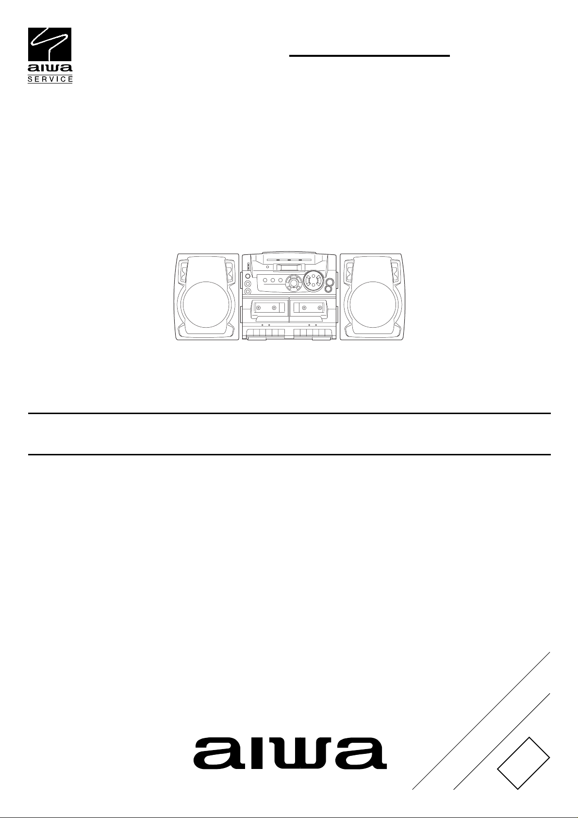
CA-DW537
U(S),LH(S)
SERVICE MANUAL
COMPACT DISC CARRY
COMPONENT SYSTEM
This Service Manual is the “Revision Publishing” and replaces “Simple Manual”
CA-DW537<U(S),LH(S)>(S/M Code No. 09-003-342-1T1).
• BASIC TAPE MECHANISM : ZZM-2 YPR3NF
• BASIC CD MECHANISM : DA11T3C
S/M Code No. 09-003-342-1R1
REVISION
DATA
Page 2
SPECIFICATIONS
LH MODEL U MODEL
Design and specifications are subject to change
•
without notice
.
Design and specifications are subject to change
•
without notice
.
ACCESSORIES/PACKAGE LIST
REF. NO PART NO. KANRI DESCRIPTION
1 8A-CT6-902-010 IB,LH(ESP)FM<LH<S>>
1 8A-CT6-903-010 IB,U(ESF)FM<U<S>>
2 8Z-CDK-962-010 RC UNIT,RC-ZAT02(VS)
2 8Z-CK4-962-010 RC UNIT,RC-ZAT04 (VS)
!
3 87-A80-036-010 AC CORD SET ASSY,E W/FLTR VOL
!
3 87-A80-033-010 AC CORD SET,D BLK
!
3 87-A80-109-010 AC CORD,HK7281 BLK U<U<S>>
!
4 87-A90-312-010 PLUG,CONVERSION WTN-1157R1<LH<S>>
NO.
<LH<S>>
2
Page 3
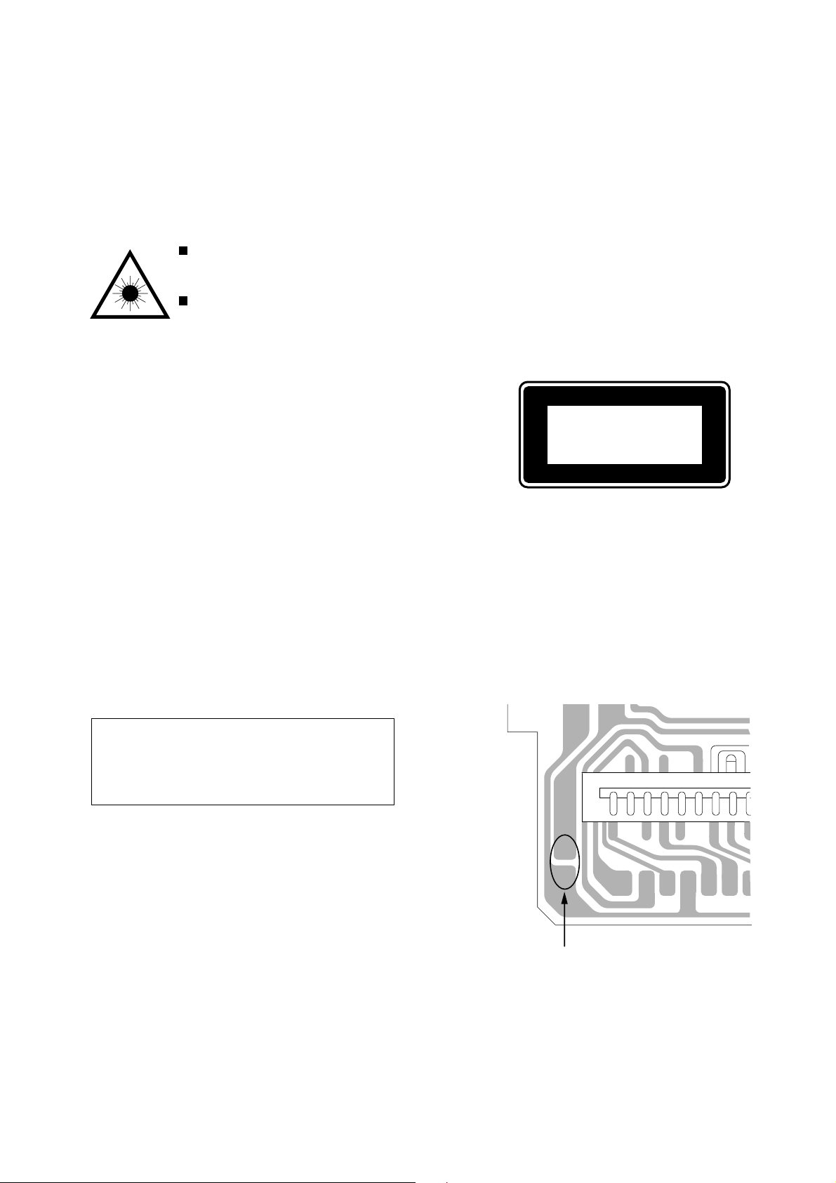
PROTECTION OF EYES FROM LASER BEAM DURING SERVICING
Solder
PICK-UP Assy P.C.B
This set employs laser. Therefore, be sure to follow carefully the
instructions below when servicing.
WARNING!
WHEN SERVICING, DO NOT APPROACH THE LASER EXIT
WITH THE EYE TOO CLOSELY. IN CASE IT IS NECESSARY TO
CONFIRM LASER BEAM EMISSION. BE SURE TO OBSERVE
FROM A DISTANCE OF MORE THAN 30cm FROM THE
SURFACE OF THE OBJECTIVE LENS ON THE OPTICAL
PICK-UP BLOCK.
Caution: Invisible laser radiation when
open and interlocks defeated avoid exposure to beam.
Advarsel:Usynling laserståling ved åbning,
når sikkerhedsafbrydere er ude af funktion.
Undgå udsættelse for stråling.
VAROITUS!
Laiteen Käyttäminen muulla kuin tässä käyttöohjeessa mainitulla tavalla saattaa altistaa käyt-täjän turvallisuusluokan 1 ylittävälle näkymättömälle lasersäteilylle.
VARNING!
Om apparaten används på annat sätt än vad som specificeras i
denna bruksanvising, kan användaren utsättas för osynling
laserstrålning, som överskrider gränsen för laserklass 1.
CAUTION
Use of controls or adjustments or performance of procedures
other than those specified herein may result in hazardous
radiation exposure.
ATTENTION
L'utilisation de commandes, réglages ou procédures autres que
ceux spécifiés peut entraîner une dangereuse exposition aux
radiations.
ADVARSEL!
Usynlig laserståling ved åbning, når sikkerhedsafbrydereer ude
af funktion. Undgå udsættelse for stråling.
This Compact Disc player is classified as a CLASS 1 LASER
product.
The CLASS 1 LASER PRODUCT label is located on the rear
exterior.
CLASS 1
KLASSE 1
LUOKAN 1
KLASS 1
LASER PRODUCT
LASER PRODUKT
LASER LAITE
LASER APPARAT
Precaution to replace Optical block
(SF-P101NR)
Body or clothes electrostatic potential could ruin
laser diode in the optical block. Be sure ground
body and workbench, and use care the clothes
do not touch the diode.
1) After the connection, remove solder shown in
the right figure.
3
Page 4

ELECTRICAL MAIN PARTS LIST
REF. NO PART NO. KANRI DESCRIPTION
IC
87-A21-550-010 IC,TA2149N
87-A21-185-040 C-IC,LC72121M
87-A21-090-010 IC,LA4600
87-A21-520-040 C-IC,M61509FP
87-020-828-010 IC,BA3416BL
87-001-440-010 IC,BA15218N
87-A20-446-010 C-IC,LA9241ML
87-A20-459-010 C-IC,LC78622ED
87-A21-093-010 IC,LA6541D
8A-CH4-661-010 C-IC,LC867132V-5P07
87-A20-914-010 IC,SPS-442-1-F
TRANSISTOR
89-327-143-080 TR,2SC2714 (0.1W)
87-026-447-080 TR,2SC1740S R
89-111-624-080 TR,2SA1162Y
87-026-213-080 CHIP-TR,DTC114YK
89-327-125-080 CHIP TR,2SC2712GR
89-320-011-080 TR,2SC2001 (15W)
87-026-462-080 TR,2SC1740 S(RS 0.3W)
87-026-291-080 TR,DTC124XS
89-109-332-380 TR,2SA933RS
89-113-187-080 TR,2SA1318TU
87-026-239-080 C-TR,DTC114TK
87-026-210-080 C-TR,DTC144EK
89-112-965-080 TR,2SA1296 (0.75W)
87-026-463-080 TR,2SA933S (0.3W)
87-A30-226-010 TR,2SB1655E
89-318-154-080 TR,2SC1815 (0.4W)
87-026-291-010 TR,DTC124XS
87-026-463-010 TR,2SA933S,RS
87-026-464-010 TR,DTC114TS
87-026-610-080 TR,KTC3198GR
89-322-405-080 TR,2SC2240GR
DIODE
87-020-465-080 DIODE,1SS133 (110MA)
87-A40-616-070 VARI-CAP,SVC384(S/T)
87-A40-128-080 C-VARI-CAP,HVU202A
87-017-072-080 ZENER,HZS3B1
87-A40-466-080 ZENER,MTZJ2.7A
87-070-345-080 DIODE,IN4148
87-A40-648-080 ZENER,MTZJ8.2A
87-001-731-080 ZENER,HZS6C2L
87-027-399-080 ZENER,HZ7A3L (200MA)<U<S>>
87-027-607-080 ZENER,HZ7B3L<LH<S>>
84-RM1-695-010 DIODE,1N4148
87-A40-465-010 DIODE,FR202
MAIN C.B
C1 87-010-314-080 C-CAP,S 22P-50V
C2 87-010-316-080 C-CAP,S 33P-50 CH
C3 87-010-314-080 C-CAP,S 22P-50V
C5 87-016-669-080 C-CAP,S 0.1-25 K B
C6 87-010-313-080 CAP, CHIP 18P
C7 87-014-049-080 CAP,PP 470P-100 J
C8 87-012-349-080 C-CAP,S 1000P-50 CH
C10 87-010-197-080 CAP, CHIP 0.01 DM
C11 87-010-197-080 CAP, CHIP 0.01 DM
C12 87-010-197-080 CAP, CHIP 0.01 DM
C13 87-010-150-080 C-CAP,S 6P-50 CH<U<S>>
C14 87-010-303-080 C-CAP,S 330P-50CH
C15 87-012-349-080 C-CAP,S 1000P-50 CH
C16 87-010-374-080 CAP, ELECT 47-10V
C17 87-010-194-080 CAP, CHIP 0.047
NO.
REF. NO PART NO. KANRI DESCRIPTION
C18 87-015-835-080 C-CAP,0.047 D
C19 87-010-263-080 CAP, ELECT 100-10V
C20 87-010-404-080 CAP, ELECT 4.7-50V
C21 87-010-197-080 CAP, CHIP 0.01 DM
C22 87-010-197-080 CAP, CHIP 0.01 DM
C23 87-010-197-080 CAP, CHIP 0.01 DM
C25 87-016-460-080 C-CAP,S 0.22-16 B
C27 87-A11-067-080 C-CAP,S 1-10 K B
C28 87-016-669-080 C-CAP,S 0.1-25 K B
C29 87-016-669-080 C-CAP,S 0.1-25 K B
C30 87-010-220-080 C-CAP,S 0.018-25 K B<LH<S>>
C30 87-010-593-080 C-CAP,S 0.027-16 K R GRM<U<S>>
C31 87-010-220-080 C-CAP,S 0.018-25 K B<LH<S>>
C31 87-010-593-080 C-CAP,S 0.027-16 K R GRM<U<S>>
C33 87-012-353-080 C-CAP, 0.33-16 K R
C34 87-012-353-080 C-CAP, 0.33-16 K R
C35 87-015-819-080 CAPACITOR,0.01
C36 87-010-263-080 CAP, ELECT 100-10V
C37 87-010-197-080 CAP, CHIP 0.01 DM
C38 87-010-374-080 CAP, ELECT 47-10V
C39 87-010-404-080 CAP, ELECT 4.7-50V
C40 87-010-197-080 CAP, CHIP 0.01 DM
C41 87-012-349-080 C-CAP,S 1000P-50 CH
C42 87-012-349-080 C-CAP,S 1000P-50 CH
C43 87-012-349-080 C-CAP,S 1000P-50 CH
C44 87-010-312-080 C-CAP,S 15P-50 CH<U<S>>
C45 87-010-312-080 C-CAP,S 15P-50 CH
C46 87-010-197-080 CAP, CHIP 0.01 DM
C47 87-010-197-080 CAP, CHIP 0.01 DM
C48 87-010-197-080 CAP, CHIP 0.01 DM
C49 87-012-140-080 CAP 470P
C50 87-010-197-080 CAP, CHIP 0.01 DM
C71 87-010-197-080 CAP, CHIP 0.01 DM
C72 87-010-263-080 CAP, ELECT 100-10V
C73 87-010-197-080 CAP, CHIP 0.01 DM
C75 87-010-197-080 CAP, CHIP 0.01 DM<U<S>>
C91 87-010-197-080 CAP, CHIP 0.01 DM
C92 87-010-197-080 CAP, CHIP 0.01 DM
C93 87-010-197-080 CAP, CHIP 0.01 DM
C99 87-018-131-080 CAP,TC U 1000P-50 K B
C215 87-A10-201-080 C-CAP,S 0.33-16 K B
C216 87-012-353-080 C-CAP, 0.33-16 K R
C231 87-015-632-080 C-CAP,0.015-50 B
C232 87-015-632-080 C-CAP,0.015-50 B
C233 87-012-353-080 C-CAP, 0.33-16 K R
C234 87-012-353-080 C-CAP, 0.33-16 K R
C235 87-015-785-080 C-CAP, 0.1-25 Z F
C236 87-015-785-080 C-CAP, 0.1-25 Z F
C237 87-010-408-080 CAP,E 47-50 M 11L SME
C238 87-010-248-080 CAP, ELECT 220-10V
C239 87-010-213-080 C-CAP,S 0.015-50 B
C239 87-010-197-080 CAP, CHIP 0.01 DM
C240 87-010-197-080 CAP, CHIP 0.01 DM
C241 87-010-401-080 CAP, ELECT 1-50V
C242 87-010-401-080 CAP, ELECT 1-50V
C243 87-010-401-080 CAP, ELECT 1-50V
C244 87-010-401-080 CAP, ELECT 1-50V
C245 87-010-401-080 CAP, ELECT 1-50V
C246 87-010-401-080 CAP, ELECT 1-50V
C247 87-010-404-080 CAP, ELECT 4.7-50V
C248 87-010-404-080 CAP, ELECT 4.7-50V
C251 87-010-405-080 CAP, ELECT 10-50V
C261 87-010-401-080 CAP, ELECT 1-50V
C262 87-010-401-080 CAP, ELECT 1-50V
C264 87-010-178-080 CHIP CAP 1000P
C266 87-010-545-080 CAP, ELECT 0.22-50V
C267 87-010-545-080 CAP, ELECT 0.22-50V
C271 87-010-237-080 CAP, ELECT 1000-16V
C272 87-010-237-080 CAP, ELECT 1000-16V
C277 87-010-404-080 CAP, ELECT 4.7-50V
NO.
4
Page 5

REF. NO PART NO. KANRI DESCRIPTION
C278 87-010-263-080 CAP, ELECT 100-10V
C279 87-010-112-080 CAP, ELECT 100-16V
C280 87-010-198-080 CAP, CHIP 0.022
C291 87-010-404-080 CAP, ELECT 4.7-50V
C293 87-010-404-080 CAP, ELECT 4.7-50V
C301 87-012-157-080 C-CAP,S 330P-50 CH
C302 87-012-157-080 C-CAP,S 330P-50 CH
C303 87-010-177-080 C-CAP,S 820P-50 SL
C304 87-010-177-080 C-CAP,S 820P-50 SL
C305 87-010-374-080 CAP, ELECT 47-10V
C306 87-010-374-080 CAP, ELECT 47-10V
C307 87-010-382-080 CAP, ELECT 22-25V
C308 87-010-405-080 CAP, ELECT 10-50V
C309 87-010-404-080 CAP, ELECT 4.7-50V
C310 87-010-404-080 CAP, ELECT 4.7-50V
C311 87-010-248-080 CAP, ELECT 220-10V
C312 87-010-374-080 CAP, ELECT 47-10V
C313 87-015-834-080 C-CAP,0.033-25
C314 87-015-834-080 C-CAP,0.033-25
C315 87-010-401-080 CAP, ELECT 1-50V
C316 87-010-401-080 CAP, ELECT 1-50V
C317 87-010-382-080 CAP, ELECT 22-25V
C318 87-010-382-080 CAP, ELECT 22-25V
C319 87-010-405-080 CAP, ELECT 10-50V
C320 87-010-405-080 CAP, ELECT 10-50V
C321 87-012-157-080 C-CAP,S 330P-50 CH
C322 87-012-157-080 C-CAP,S 330P-50 CH
C323 87-010-197-080 CAP, CHIP 0.01 DM
C324 87-010-197-080 CAP, CHIP 0.01 DM
C325 87-010-180-080 C-CER 1500P
C326 87-010-180-080 C-CER 1500P
C327 87-010-404-080 CAP, ELECT 4.7-50V
C328 87-010-178-080 CHIP CAP 1000P
C329 87-010-182-080 C-CAP,S 2200P-50 B
C330 87-010-180-080 C-CAP,S 1500P-50 K B
C331 87-010-263-080 CAP,E 100-10 M 11L
C332 87-010-178-080 CHIP CAP 1000P
C334 87-012-155-080 C-CAP 180P-50CH
C341 87-012-157-080 C-CAP,S 330P-50 CH
C342 87-012-157-080 C-CAP,S 330P-50 CH
C343 87-012-157-080 C-CAP,S 330P-50 CH
C344 87-010-303-080 C-CAP,S 330P-50CH
C363 87-010-182-080 C-CAP,S 2200P-50 B
C364 87-010-182-080 C-CAP,S 2200P-50 B
C401 87-010-403-080 CAP, ELECT 3.3-50V
C402 87-010-197-080 CAP, CHIP 0.01 DM
C403 87-010-263-080 CAP, ELECT 100-10V
C404 87-010-248-080 CAP, ELECT 220-10V
C405 87-010-197-080 CAP, CHIP 0.01 DM
C406 87-010-374-080 CAP, ELECT 47-10V
C407 87-010-178-080 CHIP CAP 1000P
C408 87-010-198-080 CAP, CHIP 0.022
C409 87-010-248-080 CAP, ELECT 220-10V
C410 87-010-263-080 CAP, ELECT 100-10V
C411 87-A11-177-080 C-CAP,S 0.15-16 K B
C412 87-010-401-080 CAP, ELECT 1-50V
C413 87-016-369-080 C-CAP,S 0.033-25 B K
C414 87-010-405-080 CAP, ELECT 10-50V
C416 87-010-545-080 CAP, ELECT 0.22-50V
C417 87-012-157-080 C-CAP,S 330P-50 CH
C418 87-010-213-080 C-CAP,S 0.015-50 B
C419 87-A11-608-080 C-CAP,S 0.33-25 K B
C420 87-016-369-080 C-CAP,S 0.033-25 B K
C421 87-A11-177-080 C-CAP,S 0.15-16 K B
C422 87-010-184-080 CHIP CAPACITOR 3300P(K)
C423 87-010-194-080 CAP, CHIP 0.047
C424 87-016-460-080 C-CAP,S 0.22-16 K B
C425 87-010-176-080 C-CAP,S 680P-50 SL
C426 87-A11-608-080 C-CAP,S 0.33-25 K B
C428 87-010-197-080 CAP, CHIP 0.01 DM
NO.
REF. NO PART NO. KANRI DESCRIPTION
C429 87-010-186-080 CAP,CHIP 4700P
C430 87-012-156-080 C-CAP,S 220P-50 CH
C431 87-010-545-080 CAP, ELECT 0.22-50V
C432 87-010-374-080 CAP, ELECT 47-10V
C433 87-010-401-080 CAP, ELECT 1-50V
C434 87-010-184-080 CHIP CAPACITOR 3300P(K)
C435 87-010-197-080 CAP, CHIP 0.01 DM
C436 87-010-374-080 CAP, ELECT 47-10V
C437 87-010-404-080 CAP, ELECT 4.7-50V
C438 87-012-368-080 C-CAP,S 0.1-50 F
C439 87-010-178-080 CHIP CAP 1000P
C440 87-010-145-080 C-CAP,S 1P-50 CH
C441 87-010-197-080 CAP, CHIP 0.01 DM
C442 87-010-313-080 CAP, CHIP 18P
C445 87-012-368-080 C-CAP,S 0.1-50 F
C446 87-012-368-080 C-CAP,S 0.1-50 F
C447 87-012-368-080 C-CAP,S 0.1-50 F
C448 87-010-315-080 C-CAP,S 27P-50 CH
C450 87-010-305-080 C-CAP 470P-50CH
C451 87-012-156-080 C-CAP,S 220P-50 CH
C455 87-010-247-080 CAP, ELECT 100-50V
C457 87-010-312-080 C-CAP,S 15P-50 CH
C458 87-010-312-080 C-CAP,S 15P-50 CH
C459 87-010-263-080 CAP, ELECT 100-10V
C460 87-015-819-080 CAPACITOR,0.01
C461 87-010-197-080 CAP, CHIP 0.01 DM
C462 87-010-248-080 CAP, ELECT 220-10V
C463 87-018-134-080 CAPACITOR,TC-U 0.01-16
C465 87-010-404-080 CAP, ELECT 4.7-50V
C466 87-012-368-080 C-CAP,S 0.1-50 F
C467 87-010-263-080 CAP, ELECT 100-10V
C469 87-012-154-080 C-CAP,S 150P-50 CH
C470 87-010-544-080 CAP, ELECT 0.1-50V
C472 87-010-858-080 C-CAP,0.1-250 K
C473 87-010-858-080 C-CAP,0.1-250 K
C474 87-010-858-080 C-CAP,0.1-250 K
C475 87-015-819-080 CAPACITOR,0.01
C476 87-010-236-080 CAP,E 1000-10 SME
C477 87-010-197-080 CAP, CHIP 0.01 DM
C478 87-010-263-080 CAP, ELECT 100-10V
C479 87-010-197-080 CAP, CHIP 0.01 DM
C480 87-010-221-080 CAP, ELECT 470-10V
C481 87-010-405-080 CAP, ELECT 10-50V
C482 87-010-405-080 CAP, ELECT 10-50V
C483 87-012-156-080 C-CAP,S 220P-50 CH
C484 87-012-156-080 C-CAP,S 220P-50 CH
C489 87-012-368-080 C-CAP,S 0.1-50 F
C490 87-012-368-080 C-CAP,S 0.1-50 F
C491 87-015-819-080 CAPACITOR,0.01
C492 87-010-221-080 CAP, ELECT 470-10V
C493 87-010-197-080 CAP, CHIP 0.01 DM
C494 87-018-134-080 CAPACITOR,TC-U 0.01-16
C500 87-010-197-010 CAP, S 0.01-25
C501 87-016-589-090 CAP,E 3300-25 SSL
C506 87-010-404-080 CAP, ELECT 4.7-50V
C507 87-010-401-080 CAP, ELECT 1-50V
C508 87-010-221-080 CAP, ELECT 470-10V
C510 87-010-248-080 CAP, ELECT 220-10V
C511 87-010-374-080 CAP, ELECT 47-10V
C512 87-010-385-080 CAP, ELECT 220-25V
C514 87-010-248-080 CAP, ELECT 220-10V
C515 87-010-197-010 CAP, S 0.01-25
C516 87-010-384-080 CAP, ELECT 100-25V
C517 87-010-197-010 CAP, S 0.01-25
C521 87-010-197-080 CAP, CHIP 0.01 DM
C522 87-010-263-080 CAP, ELECT 100-10V
C544 87-010-405-080 CAP, ELECT 10-50V<LH<S>>
C761 87-010-263-080 CAP, ELECT 100-10V
C2001 87-012-349-080 C-CAP,S 1000P-50 CH
C2002 87-012-349-080 C-CAP,S 1000P-50 CH
NO.
5
Page 6

REF. NO PART NO. KANRI DESCRIPTION
C2003 87-012-349-080 C-CAP,S 1000P-50 CH
C2004 87-012-349-080 C-CAP,S 1000P-50 CH
C2005 87-012-349-080 C-CAP,S 1000P-50 CH
C4001 87-012-368-080 C-CAP,S 0.1-50 F
C4002 87-010-322-080 C-CAP,S 100P-50 CH
C4003 87-010-297-080 CAP CHIO 100P
C4004 87-010-322-080 C-CAP,S 100P-50 CH
C4005 87-010-297-080 CAP CHIO 100P
C4006 87-010-322-080 C-CAP,S 100P-50 CH
C4010 87-012-368-080 C-CAP,S 0.1-50 F
C4011 87-012-349-080 C-CAP,S 1000P-50 CH
C4012 87-012-349-080 C-CAP,S 1000P-50 CH
C4013 87-012-349-080 C-CAP,S 1000P-50 CH
CF1 87-A91-094-010 FLTR,CDA10.7 MG80A
CF2 82-785-747-080 CF,MS2 GHY,R
CF3 82-785-747-080 CF,MS2 GHY,R
CN201 87-049-469-010 CONN,4P V
CN301 88-CT6-604-010 CONN ASSY,4P PH
CN302 88-CT6-605-010 CONN ASSY,5P RPH
CN401 87-A60-424-010 CONN,16P V TOC-B
CN501 87-049-919-010 CONN,3P EH V WHT
CN751 88-CT6-608-010 CONN ASSY,8P MO
D201 87-020-465-080 DIODE,1SS133 (110MA)
J251 8A-CT9-630-010 JACK,MIC ST SW
L2 87-A50-560-010 COIL,FM BPF(ACD)
L4 87-A50-420-010 COIL,MW OSC(SYN)
L5 87-A50-566-010 COIL,FM RF EX(ACH)
L6 87-A50-568-010 COIL,FM OSC EX(ACH)
L7 87-A91-308-010 FLTR,PCFAZH- 450T (TOK)
L8 87-005-849-080 COIL,10UH(CECS)
L9 87-005-849-080 COIL,10UH(CECS)
L090 87-003-152-080 COIL, 100UH
L330 88-CT6-620-010 REC OSC
L401 87-003-102-080 COIL, 10UH
L404 87-003-152-080 COIL, 100UH
!
R488 87-A00-296-080 C-RES,100K-1/8W F
!
R761 87-029-019-010 RES, FUSEIBLE 1/2W-2.2
SFR430 87-024-437-080 SFR, 100 K H
SFR761 87-024-524-080 SFR, 22 K V
SW301 88-CT6-619-010 BACK SLIDE SW 6P2T SHORTIN
TC1 87-011-254-080 TRIMER,20P LAR
X1 87-A70-061-010 VIB,XTAL 4.500MHZ CSA-309
X401 8Z-CD5-633-010 VIB, CER16.93MHZ FCR16.93M2
FRONT C.B
C601 87-010-313-080 CAP, CHIP 18P
C602 87-010-315-080 C-CAP,S 27P-50 CH
C603 87-010-317-080 C-CAP,S 39P-50 CH
C604 87-010-314-080 C-CAP,S 22P-50V
C605 87-010-316-080 C-CAP,S 33P-50 CH
C606 87-012-350-080 C-CAP,1-25 F
C607 87-010-197-080 CAP, CHIP 0.01 DM
C608 87-016-669-080 C-CAP,S 0.1-25 K B
C609 87-016-669-080 C-CAP,S 0.1-25 K B
C610 87-010-263-080 CAP, ELECT 100-10V
C611 87-016-669-080 C-CAP,S 0.1-25 K B
C612 87-010-221-080 CAP, ELECT 470-10V
C613 87-010-402-080 CAP, ELECT 2.2-50V
C614 87-010-196-080 CHIP CAPACITOR,0.1-25
C615 87-010-400-080 CAP, ELECT 0.47-50V
C616 87-010-401-080 CAP, ELECT 1-50V
C617 87-010-179-080 CAP,CHIP S B1200P
C618 87-010-263-080 CAP, ELECT 100-10V
C762 87-010-198-080 CAP, CHIP 0.022
C765 87-016-669-080 C-CAP,S 0.1-25 K B
C830 87-010-197-080 CAP, CHIP 0.01 DM
C831 87-010-197-080 CAP, CHIP 0.01 DM
C832 87-010-181-080 CAP,CHIP S 1800P
C833 87-010-178-080 CHIP CAP 1000P
NO.
REF. NO PART NO. KANRI DESCRIPTION
C834 87-010-404-080 CAP, ELECT 4.7-50V
C835 87-010-544-080 CAP, ELECT 0.1-50V
C836 87-010-178-080 CHIP CAP 1000P
C837 87-010-178-080 CHIP CAP 1000P
C838 87-010-401-080 CAP, ELECT 1-50V
C839 87-010-401-080 CAP, ELECT 1-50V
C840 87-010-221-080 CAP, ELECT 470-10V
C841 87-010-401-080 CAP, ELECT 1-50V
C842 87-012-140-080 CAP 470P
C844 87-010-401-080 CAP, ELECT 1-50V
C4008 87-010-198-080 CAP, CHIP 0.022
C4009 87-010-198-080 CAP, CHIP 0.022
C6003 87-010-263-080 CAP, ELECT 100-10V
C6004 87-010-198-080 CAP, CHIP 0.022
C6005 87-010-198-080 CAP, CHIP 0.022
C6006 87-010-198-080 CAP, CHIP 0.022
C6007 87-010-198-080 CAP, CHIP 0.022
C6009 87-010-198-080 CAP, CHIP 0.022
C6010 87-010-198-080 CAP, CHIP 0.022
C6011 87-010-198-080 CAP, CHIP 0.022
C6012 87-012-349-080 C-CAP,S 1000P-50 CH
CN601 87-A60-109-010 CONN,2P V S2M-2W
J801 8A-CT9-630-010 JACK,MIC ST SW
L601 87-003-149-080 COIL,47UH
LCD601 8A-CT9-620-010 LCD,HLC7107ACT-9
LED605 8Z-CT6-632-010 LED,L-934LID
LED606 8Z-CT6-632-010 LED,L-934LID
LED607 8Z-CT6-632-010 LED,L-934LID
LED608 8Z-CT6-632-010 LED,L-934LID
LED609 8Z-CT6-632-010 LED,L-934LID
LED610 8Z-CT6-632-010 LED,L-934LID
S602 8Z-CT6-636-010 SW,TACT EVQJAC04M
S603 8Z-CT6-636-010 SW,TACT EVQJAC04M
S604 8Z-CT6-636-010 SW,TACT EVQJAC04M
S605 8Z-CT6-636-010 SW,TACT EVQJAC04M
S606 8Z-CT6-636-010 SW,TACT EVQJAC04M
S607 8Z-CT6-636-010 SW,TACT EVQJAC04M
S608 8Z-CT6-636-010 SW,TACT EVQJAC04M
S609 8Z-CT6-636-010 SW,TACT EVQJAC04M
S610 8Z-CT6-636-010 SW,TACT EVQJAC04M
S611 8Z-CT6-636-010 SW,TACT EVQJAC04M
S612 8Z-CT6-636-010 SW,TACT EVQJAC04M
S613 8Z-CT6-636-010 SW,TACT EVQJAC04M
S614 8Z-CT6-636-010 SW,TACT EVQJAC04M
S615 8Z-CT6-636-010 SW,TACT EVQJAC04M
S616 8Z-CT6-636-010 SW,TACT EVQJAC04M
VR801 87-A90-768-010 VR,RTRY 10KAX1 1 H
X601 87-030-273-010 VIB,XTAL 32.768K5PPM
X602 87-A70-070-080 VIB,CER 5.76MHZ CRHF
PWR C.B
C901 87-A10-577-080 CAP,CER 0.022-50 Z YF
C902 87-A10-577-080 CAP,CER 0.022-50 Z YF
C903 87-A10-577-080 CAP,CER 0.022-50 Z YF
C904 87-A10-577-080 CAP,CER 0.022-50 Z YF
!
F901 87-035-139-010 FUSE, 2.5A T 250V<LH<S>>
!
F901 87-035-367-010 FUSE, 3.15A 250V<U<S>>
!
F901 87-035-486-010 FUSE,2.5A 125V D UL
!
FC901 87-A90-160-080 FUSE CLAMP,FC 51F
!
FC902 87-A90-160-080 FUSE CLAMP,FC 51F
J901 87-A60-177-010 JACK,AC U W/SW<U<S>>
LED C.B
CN603 87-A61-265-080 CONN,4P H,LED-PWB
LED602 8Z-CT6-632-010 LED,L-934LID
LED603 8Z-CT6-632-010 LED,L-934LID
LED604 8Z-CT6-632-010 LED,L-934LID
NO.
6
Page 7
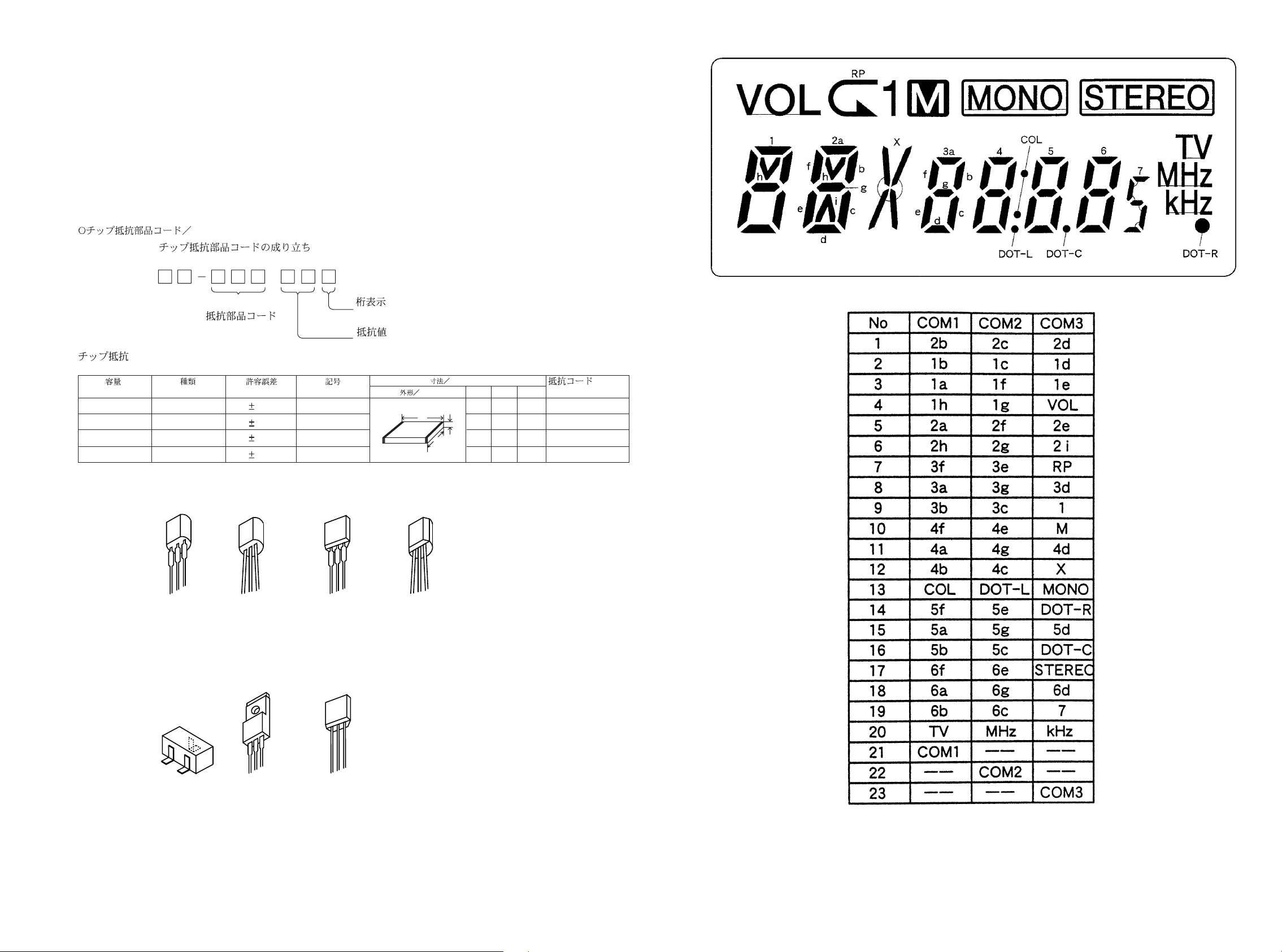
LCD DISPLAY
REF. NO PART NO. KANRI DESCRIPTION
MOTOR C.B
M2 9X-262-576-910 MOTOR GEAR ASSY
PIN3 91-564-722-110 CONNECTOR 6P
SW1 91-572-085-120 LEAF SW
• Regarding connectors, they are not stocked as they are not the initial order items.
The connectors are available after they are supplied from connector manufacturers upon the order is received.
NO.
CHIP RESISTOR PART CODE
Chip Resistor Part Coding
88
A
Resistor Code
Chip resistor
Wattage Type Tolerance
1/16W 1005 5% CJ
1/16W
1/10W
1/8W
1608
2125
3216
5%
5%
5%
Symbol
Figure
Value of resistor
CJ
CJ
CJ
Form
L
W
Dimensions (mm)
LW t
1.0 0.5 0.35 104
t
1.6 0.8 0.45
2 1.25 0.45
1.6
0.55
3.2
Resistor Code
108
118
128
: A
: A
TRANSISTOR ILLUSTRATION
ECB ECB ECB ECB
2SA1296
2SC2001
2SC1815
2SC2240
KTC3198
C
B
E
2SA1162
2SB1655
2SC2712
2SC2714
DTA114YK
DTC114TK
DTC114YK
DTC144EK
2SA933
2SC1740
DTC114TS
ECBBCE
DTC124XS
2SA1318
87
Page 8
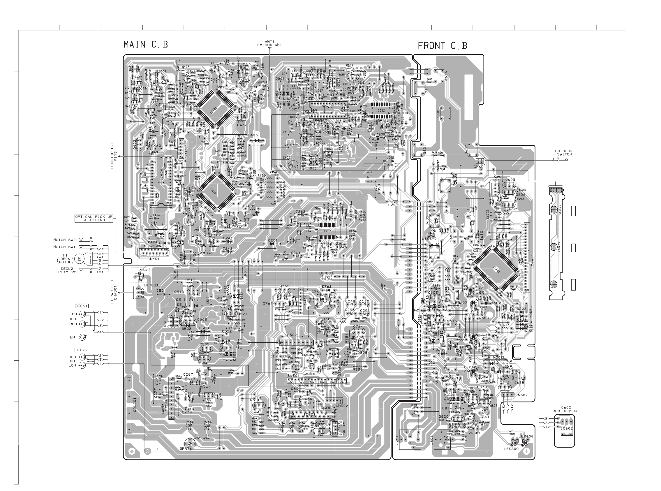
WIRING-1 (MAIN/FRONT)
1
A
B
C
234567
8
9
10
11 12 13
14
D
E
LED C. B
14
CN603
JAZZ
POP
F
ROCK
LED602 LED603 LED604
G
H
I
J
K
109
Page 9
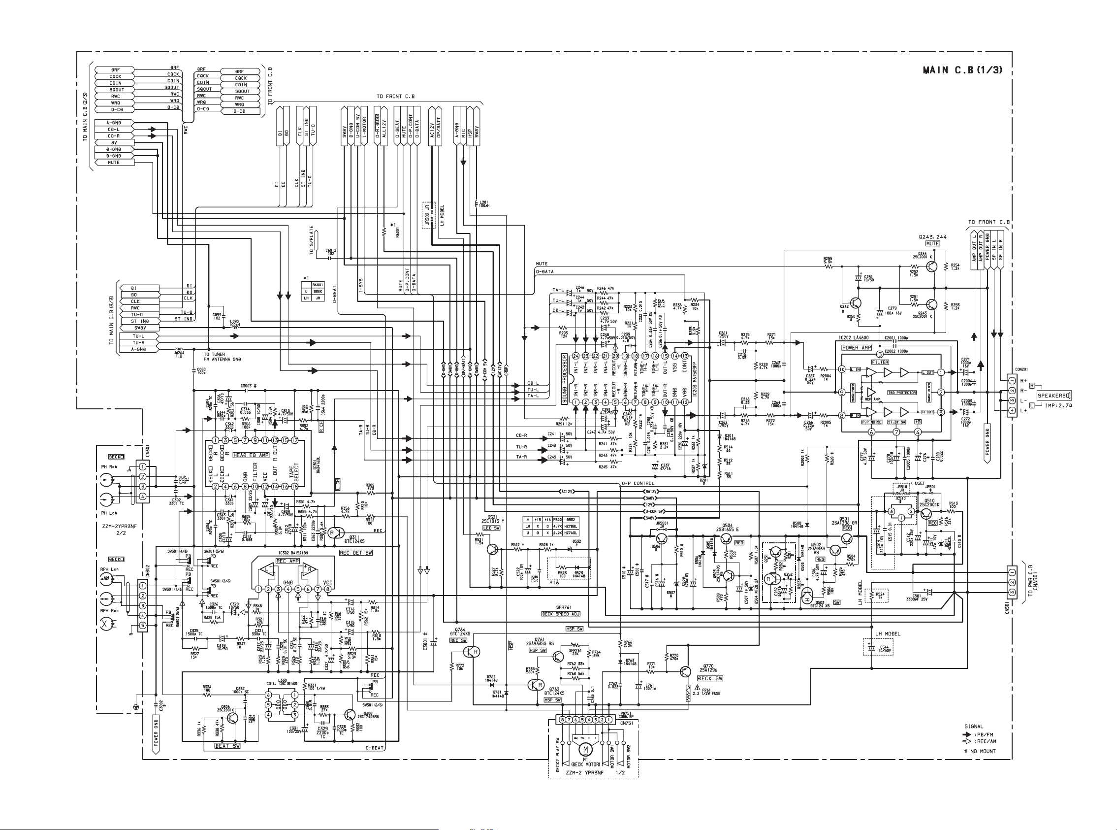
SCHEMATIC DIAGRAM-1 (MAIN)
1211
Page 10
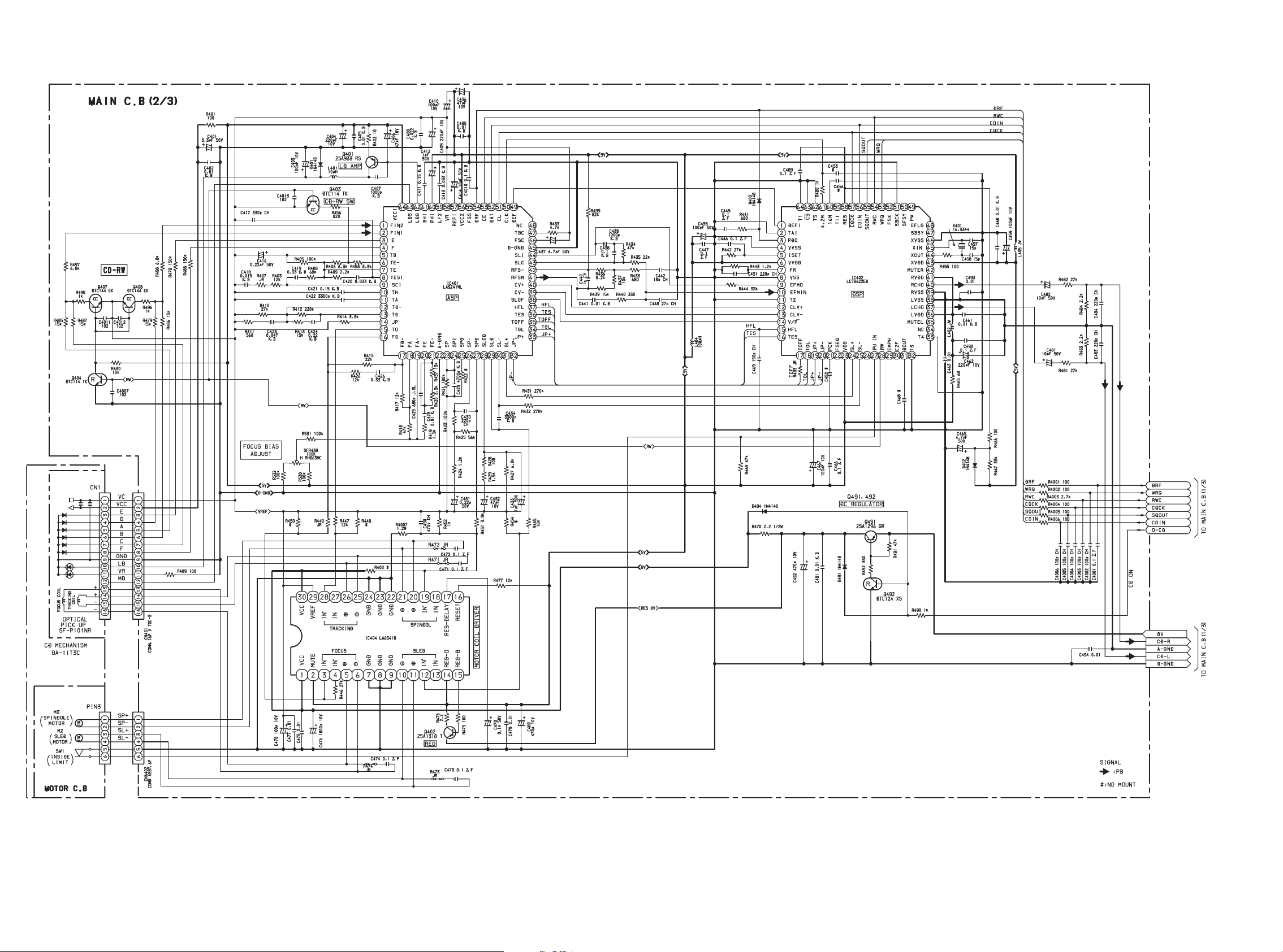
SCHEMATIC DIAGRAM-2 (CD)
1413
Page 11

SCHEMATIC DIAGRAM-3 (TUNER)
1615
Page 12

SCHEMATIC DIAGRAM-4 (FRONT)
1817
Page 13

WIRING-2 (PWR/MOTOR)
1
A
234567
MOTOR C.B
M2
SCHEMATIC DIAGRAM-5 (POWER)
B
C
CNA402
TO MAIN C.B
D
E
F
+
_
SW1
PIN3
M2
(SLED MOTOR)
SW1
(INSIDE LIMIT SW)
(SPINDLE MOTOR)
_
M3
M3
+
G
H
I
J
K
2019
Page 14

ELECTRICAL ADJUSTMENT
PRACTICAL SERVICE FIGURE
FRONTC .B MAINC.B
IC001
C39
L006
24 4
L007
L004
2
1
L005
TC001
3
L003
3
5
9
BAR ANT
SFR430
< TUNER SECTION >
1. AM IF Adjustment
L007 ....................................................................... 450kHz
2. AM VT Adjustment
Settings: • Test point: C39+
• Adjustment location: L004
Method: Set to AM 1710kHz adjust L004 so that the test
point becomes 5.6V±0.2V
3. AM Tracking Adjustment
L003 ....................................................................... 600kHz
TC001................................................................... 1400kHz
4. FM VT Adjustment
Settings: • Test point: C39+
• Adjustment location: L006
Method: Set to FM 108MHz adjust L006 so that the test
point becomes 5.6V±0.2V
5. FM Tracking Adjustment
L005 ........................................................................98MHz
< TAPE SECTION >
6. Bias frequency Adjustment
L330 ............................................................. 52kHz ±1kHz
7. Tape speed Adjustment
Settings: • Test tape: MT111
• Test point: PHONES JACK (J251)
• Adjustment location: SFR761
Method: Play back the test tape and adjust so that the
output frequency is 3000Hz ±30Hz.
< TUNER SECTION >
< FM SECTION >
Sensitivity: Less than 22dB (87.5MHz)
(THD 3%) Less than 22dB (98.0MHz)
Less than 22dB (108.0MHz)
Signal to Noise Ratio: More than 55dB (at 98.0MHz)
(Input 54dB)
Distortion: Less than 3.0% (at 98.0MHz)
(Input 54dB)
Intermediate frequency: 10.7MHz ±0.3MHz
Stereo separation: More than 18dB (at 1kHz)
< AM SECTION >
Sensitivity: Less than 52dB (at 600kHz)
(S/N 10dB) Less than 50dB (at 1000kHz)
Less than 50dB (at 1400kHz)
Distortion: Less than 3%
(Input 74dB)
Intermediate frequency: 450kHz±5kHz
< CASSETTE SECTION >
Tape speed: 3000Hz±60Hz
Wow & flutter: Less than 0.35% (JIS RMS)
Take-up torque: 30-60g-cm (DECK 1/2)
FF torque: 55-140g-cm (DECK 1/2)
Rew torque: 55-140g-cm (DECK 1/2)
Back tension: 1-5g-cm
S/N ratio: More than 50dB (DC)
Distortion: Less than 3.0% (PB)
Noise (PB): Less than 0.9mV (DC)
Less than 15mV
(AC VOL max)
J251
78
L330
6
RPH/PH
7
SFR761
8. Azimuth Adjustment
Settings: • Test tape: TTA-320
• Test point: PHONES JACK (J251)
• Adjustment location:Azimuth adjustment
screw
Method: Play back the 8kHz signal of the test tape and
adjust screw so that the output becomes
maximum.
< CD SECTION >
9. Focus Bias Adjustment
Settings: • Test CD: TCD-782 (A-BEX)
• Test point: IC401 PIN20, PIN58
• Adjustment location: SFR430
Method: Play back the #15 of the test CD and adjust
SFR430 so that the voltage between pin20 and
pin 58 of IC401 becomes 0V ±0.1mV.
8
2221
Page 15

IC BLOCK DIAGRAM
mono. SW
Control logic
IC, LA6541D IC, M61509
IC, TA2149N IC, BA3416BL
DECK R
DECK R
R OUT
DECK L
DECK L
L OUT
TAPE SELECT
23
Page 16

VOLTAGE CHART
24
Page 17

252627
Page 18

Page 19

Page 20

IC DESCRIPTION
IC, LA9241ML
Pin No. Pin Name I/O Description
Pin to which external pickup photo diode is connected. RF signal is created by adding
1
FIN2
I
with the FIN1 pin signal. FE signal is created by subtracting from the FIN1 pin signal.
10
11
12
13
14
15
2
3
4
5
6
7
8
9
FIN1
E
F
TB
TE-
TE
TESI
SCI
TH
TA
TD-
TD
JP
TO
I
Pin to which external pickup photo diode is connected.
Pin to which external pickup photo diode is connected. TE signal is created by
I
subtracting from the F pin signal.
I
Pin to which external pickup photo diode is connected.
I
DC component of the TE signal is input.
Pin to which external resistor setting the TE signal gain is connected between the TE
I
pin.
O
TE signal output pin.
TES “Track Error Sense” comparator input pin. TE signal is passed through a band-
I
pass filter then input.
I
Shock detection signal input pin.
I
Tracking gain time constant setting pin.
O
TA amplifier output pin.
Pin to which external tracking phase compensation constants are connected between
I
the TD and VR pins.
I
Tracking phase compensation setting pin.
I
Tracking jump signal (kick pulse) amplitude setting pin.
O
Tracking control signal output pin.
16
17
18
19
20
21
22
23
24
25
26
27
28
29
FD
FD-
FA
FA-
FE
FE-
AGND
SP
SPI
SPG
SP-
SPD
SLEQ
SLD
—
O
Focusing control signal output pin.
Pin to which external focusing phase compensation constants are connected between
I
the FD and FA pins.
Pin to which external focusing phase compensation constants are connected between
I
the FD– and FA– pins.
Pin to which external focusing phase compensation constants are connected between
I
the FA and FE pins.
O
FE signal output pin.
I
Pin to which external FE signal gain setting resistor is connected between the FE pin.
Analog signal GND.
O
Signal ended output of the CV+and CV- pin input signal.
I
Spndle amp input.
I
Pin to which external spindle gain setting resistor in 12 cm mode is connected.
Pin to which external spindle phase compensation constants are connected together
I
with SPD pin.
O
Spindle control signal output pin.
I
Pin to which external sled phase compensation constants are connected.
O
Sled control signal output pin.
30, 31
32, 33
34
35
SL-, SL+
JP-, JP+
TGL
TOFF
I
Sled advance signal input pin from microprocessor.
I
Tracking jump signal input pin from DSP.
I
Tracking gain control signal input from DSP. Low gain when TGL = H.
I
Tracking off control signal input pin from DSP. Off when TOFF = H.
28
Page 21

Pin No. Pin Name I/O Description
36
TES
O
Pin from which TES signal is output to DSP.
37
38
39, 40
41
42
43
44
45
46
47
48
49
50
51
52
HFL
SLOF
CV–, CV+
RFSM
RFS-
SLC
SLI
DGND
FSC
TBC
NC
DEF
CLK
CL
DAT
O
O
O
—
O
—
O
“High Frequency Level” is used to judge whether the main beam position is on top of
bit or on top of mirror.
I
Sled servo off control input pin.
I
CLV error signal input pin from DSP.
RF output pin.
RF gain setting and EFM signal 3T compensation constant setting pin together with
I
RFSM pin.
“Slice Level Control” is the output pin which controls the RF signal data slice level by
DSP.
I
Input pin which control the data slice level by the DSP.
Digital system GND.
Output pin to which external focus search smoothing capacitor is connected.
I
“Tracking Balance Control” EF balance variable range setting pin.
No connection.
Disc defect detector output pin.
I
Reference clock input pin. 4.23 MHz of the DSP is input.
I
Microprocessor command clock input pin.
I
Microprocessor command data input pin.
53
54
55
56
57
58
59
60
61
62
63
64
CE
DRF
FSS
VCC2
REFI
VR
LF2
PH1
BH1
LDD
LDS
VCC1
—
—
—
I
Microprocessor command chip enable input pin.
O
“Detect RF” RF level detector output.
I
“Focus Search Select” focus search mode (± search/+ search) select pin.
Servo system and digital system Vcc pin.
Pin to which external bypass capacitor for reference voltage is connected.
O
Reference voltage output pin.
I
Disc defect detector time constant setting pin.
I
Pin to which external capacitor for RF signal peak holding is connected.
I
Pin to which external capacitor for RF signal bottom holding is connected.
O
APC circuit output pin.
I
APC circuit input pin.
RF system Vcc pin.
29
Page 22

IC, LC78622ED
Pin No. Pin Name I/O Description
1
DEFI
I
Defect sense signal (DEF) input pin. (Connect to 0V when not used).
2
3
4
5
6
7
8
9
10
11
12, 13
14
15
16
17
18
TAI
PDO
VVSS
ISET
VVDD
FR
VSS
EFMO
EFMIN
T2
CLV+, CLK-
___
V/P
HFL
TES
TOFF
TGL
—
—
—
I
O
For PLL.
I
Test signal input pin with built-in pull-down resistor. Be sure to connect to 0V.
Phase comparator output pin to control external VCO.
GND pin for built-in VCO. Be sure to connect to 0V.
Pin to which external resistor adjusting the PD0 output current.
Power supply pin for built-in VCO.
I
Pin for VCO frequency range adjustment.
Digital system GND. Be sure to connect to 0V.
O
For slice level control.
I
I
Test signal input pin with built-in pull-down resistor. Be sure to connect to 0V.
O
Disc motor control output. Three level output is possible using command.
Rough servo or phase control automatic selection monitoring output pin. Rough servo
O
EFM signal output pin.
EFM signal input pin.
at H. Phase servo at L.
I
Track detect signal input pin. Schmidt input.
I
Tracking error signal input pin. Schmidt input.
O
Tracking OFF output pin.
O
Tracking gain selection output pin. Gain boost at L.
19, 20
21
22
23
24
25
26
27
28
29
30
31
32, 33
34
35
36
37
JP+, JP-
PCK
FSEQ
VDD
SL+
SL-
—
PUIN
_______
RW
EMPH
C2F
DOUT
T3, T4
N.C.
MUTEL
LVDD
LCHO
—
—
—
—
O
Track jump control signal output pin. Three level output is possible using command.
O
EFM data playback clock monitoring pin 4.3218 MHz when phase is locked in.
Sync signal detection output pin. H when the sync signal which is detected from EFM
O
signal and thesync signal which is internally generated agree.
Digital system power supply pin.
O
Moves the sled to outer circumference.
O
Moves the sled to inner circumference.
Not connected.
I
CD pickup inner switch detection.
O
Read, wright signal.
O
De-emphasis monitor output pin. De-emphasis disc is being played back at H.
O
C2 flag output pin.
O
DIGITAL OUT output pin. (EIAJ format).
I
Test signal input pin with built-in pull-down resistor. Be sure to connect to 0V.
Not used. Set the pin to open.
O
L-channel 1-bit DAC.
O
L-channel mute output pin.
L-channel power supply pin.
L-channel output pin.
38
39
40
41
42
LVSS
RVSS
RCHO
RVDD
MUTER
—
—
—
O
R-channel 1-bit DAC.
O
L-channel GND. Be sure to connect to 0V.
R-channel GND. Be sure to connect to 0V.
R-channel output pin.
R-channel power supply pin.
R-channel mute output pin.
30
Page 23

Pin No. Pin Name I/O Description
43
XVDD
—
Crystal oscillator power supply pin.
44
45
46
47
48
49
50
51
52
53
54
55
56
57
58
59
XOUT
XIN
XVSS
SBSY
EFLG
PW
SFSY
SBCK
FSX
WRQ
RWC
SQOUT
COIN
___________
CQCK
RES
T11
—
O
Pin to which external 16.9344 MHz crystal oscillator is connected.
I
Crystal oscillator GND pin. Be sure to connect to 0V.
O
Subcode block sync signal output pin.
O
C1, C2, single and dual correction monitoring pin.
O
Subcode P, Q, R, S, T, U and W output pin.
O
Subcode frame sync signal output pin. Falls down when subcode enters standby.
Subcode read clock input pin. Schmidt input. (Be sure to connected to 0V when not
I
in use.)
Pin outputting the 7.35 kHz sync signal which is generated by dividing frequency of
O
crystal oscillator.
O
Subcode Q output standby output pin.
I
Read/write control input pin. Schmidt input.
O
Subcode Q output pin.
I
Command input pin from microprocessor.
I
Command input read clock or subcode read input clock from SQOUT pin
I
LC78622 reset input pin. Set this pin to L once when the main power is turned on.
O
Test signal output pin. Use this pin as open (normally L output).
60
61
62
63
64
16M
4.2M
T5
______
CS
T1
O
16.9344 MHz output pin.
O
4.2336 MHz output pin.
I
Test signal input pin with built-in pull-down resistor. Be sure to connect to 0V.
Chip select signal input pin with built-in pull-down resistor. Be sure to connect to 0V
I
while it is not controlling.
I
Test signal input pin without built-in pull-down resistor. Be sure to connect to 0V.
31
Page 24

IC, LC867132V-5P07
Pin No. Pin Name I/O Description
1
O-RMC/CE
O
CD read/write control output and TU CE.
10
11
12
13
14
15
16
17
18
2
3
4
5
6
7
8
9
O-DATA
O-CLK
—
O-CLKSFT
I-HOLD
I-RST
XT1 (IN)
XT2 (OUT)
VSS1
CF1 (IN)
CF2 (OUT)
VDD1
I-ST IND
I-KEYO
I-CD SW
I-KEY1
I-MOTOR
—
—
—
O
Data output to M62495FP.
O
Output CLK to tuner PLL.
Not Connected.
O
Clock shift output of the microcomputer.
I
Hold status detection.
I
Microcomputer reset.
I
Connected to 32.768KHZ crystal oscillator.
O
GND.
I
Connected to 6MHZ Ceramic Filter.
O
Power supply for microcomputer (+5V).
I
FM STEREO status input.
I
KEY AD input.
I
CD DOOR SW status detection input.
I
KEY AD input.
I
DECK MECHA MOTOR status input.
19
20
21
22
23
24
25
26
27
28
29
30
31
32
33
34
35
I-REC
I-FM/AM
I-TU DO
O-BASS LED
O-QS LED
O-DUBB LED
O-INT
I-DRF
I-WRQ
I-REMO
S0-PA0
S1/PA1
S2/PA2
S3/PA3
S4/PA4
S5/PA5
S6/PA6
I
REC status input.
I
FM, AM status input. (Not connected)
I
Data input from tuner PLL.
O
BASS LED ON/OFF control output. (Not connected)
O
Q-Sound LED ON/OFF control output.
O
LED control output used for high-speed dubbing.
O
INT DIODE MATRIX detection output.
I
CD RF level detection input.
I
CD sub-code Q standby input.
I
Remote control input.
O
LCD segment output.
O
LCD segment output.
O
LCD segment output.
O
LCD segment output.
O
LCD segment output.
O
LCD segment output.
O
LCD segment output.
36
37-40
41
42
43-54
55
S7/PA7
S8~S11
VDD3
VSS3
S12~S23
O-CD LED
—
—
O
LCD segment output.
O
Power supply for microcomputer (+5V).
GND.
O
LCD segment output.
O
LED ON/OFF control output for CD functions.
32
Page 25

Pin No. Pin Name I/O Description
56
O-TU LED
O
LED ON/OFF control output for TU functions.
57
58
59
60
61-63
64-66
67
68
69
70
71
72
73
74
75
76
77
O-TA LED
O-ROCK LED
O-POP LED
O-JAZZ LED
—
COM0-COM2
—
VSS2
VDD2
O-CD ON
O-TU ON
O-P.CONT
_____________________
O-H DUBB
O-MUTE
O-MO/ST
O-BEAT CONT
O-QSOUND
—
—
—
—
O
LED ON/OFF control output for TAPE functions. (Not Connected)
O
LED ON/OFF control output for ROCK.
O
LED ON/OFF control output for POP.
O
LED ON/OFF control output for JAZZ.
Not connected.
O
LCD common output.
Not connected.
GND.
Power supply for microcomputer (+5V).
O
CD PWR control output.
O
TU PWR control output.
O
Power supply control output.
O
Dubbing speed control output.
O
Main mute output.
O
FM mono/stereo output. (Not connected)
O
BEAT switch over output.
O
Q-Sound ON/OFF output. (Not connected)
78
79
80
O-COIN
I-SQOUT
O-CQCK
O
CD command output.
I
CD sub-code Q input.
O
CLK for CD commands/sub-codes.
33
Page 26

MECHANICAL PARTS LIST 1/1
REF. NO PART NO. KANRI DESCRIPTION
1 8A-CT9-006-010 WINDOW,CASS L
2 8A-CT9-002-010 BOX,CASS L
3 8A-CT9-007-010 WINDOW,CASS R
4 8A-CT9-011-010 BTN,CD A
5 86-CT9-210-010 SPR-T,CASS
6 8A-CT9-003-010 BOX,CASS R
7 87-A90-086-010 COVER,AC-SOCKET<U<S>>
8 8A-CT9-008-010 WINDOW,DISP
9 8A-CT6-004-010 CABI,FR LH<LH<S>>
9 8A-CT6-001-010 CABI,FR U<U<S>>
10 8A-CT9-021-010 LENS,POWER
11 8A-CT9-020-010 LENS,FUNC
12 8A-CT9-010-010 KEY,FUNC
13 87-A60-178-010 JACK, AC E W/SW<LH<S>>
13 87-A60-177-010 JACK, AC U W/SW<U<S>>
14 8A-CT9-022-010 LENS,GEQ
15 8A-CT9-215-010 SPR-P,REC A
16 8A-CT9-023-010 BTN,QSOUND<U<S>>
17 8A-CT9-016-010 BTN,GEQ<U<S>>
17 8A-CT9-051-010 BTN,GEQ LH<LH<S>>
18 87-063-165-010 OIL-DMPR 150
19 8A-CT9-015-010 BTN,VOL
20 8A-CT9-012-010 BTN,CD B
21 86-CT9-208-010 HLDR,KEY CASS
22 8A-CT9-013-010 KEY,CASS L
23 8A-CT9-014-010 KEY,CASS R
24 8A-CT9-216-010 SPR-P,REC B
25 86-CT9-205-110 HLDR,REC
26 88-CD6-661-010 HLDR,BAR ANT.
27 88-CT6-606-010 FFC WIRE 16P(1.0)
!
28 88-CT6-631-010 PT, H<LH<S>>
!
28 88-CT7-629-010 PT, U<U<S>>
29 88-CH6-220-010 CUSHION,CD A
30 8A-CT9-211-010 HLDR,GEQ
31 8A-CT9-205-010 HLDR,LCD
32 8A-CT9-203-010 HLDR,FUNC
33 8A-CT9-017-010 KNOB, RTRY MIC
34 8A-CT9-204-010 HLDR,POWER
35 8Z-CT6-214-010 RING,CHUCK
36 8Z-CT6-213-010 BASE,CHUCK
37 87-036-368-010 MAGNET
38 86-CT9-222-010 PLATE,MAGNET
39 86-CT9-217-010 HLDR, CHUCK A(S)
40 8A-CT9-004-010 BOX,CD
41 8A-CT9-005-010 WINDOW,CD
NO.
REF. NO PART NO. KANRI DESCRIPTION
42 88-CT6-633-010 ANT, ROD
43 87-036-389-010 SW, PUSH LOCK<LH<S>>
44 8A-CT9-201-010 CHAS,CD
45 86-CT9-121-010 HLDR,CORD RF
46 8A-CT9-212-010 SPR-T,CD
47 86-CT9-117-010 CABI,SPKR-REAR L RF
47 86-CT9-118-010 CABI,SPKR-REAR R RF
48 8A-CT9-024-010 CABI,SPKR FR
48 8A-CT9-025-010 CABI,SPKR FR R
49 88-CT6-046-010 PANEL,CD
50 87-063-164-010 OIL-DMPR 80
51 8A-CT9-027-010 FRAME,SPKR NET
52 8A-CT9-030-010 NET,SPKR
53 86-CT9-206-010 HLDR,TRANS<U<S>>
54 86-CT9-213-010 SPR-C,BATT(-)
55 86-CT9-207-010 HLDR,ANT
56 86-CT9-223-010 CUSH,FOOT
57 86-CT9-212-010 SPR-C,BATT LINK
58 8Z-CT9-044-010 CABI,REAR
59 86-CT6-036-010 HANDL,RF
60 88-CT6-022-010 COVER, HNDL
61 86-CT6-035-010 LID,BATT RF
62 86-CT9-040-010 BADGE,AIWA 63 8A-CT6-606-010 SPKR, 100 3.2HM 5W
64 8A-CT6-202-010 HLDR,LED GEQ
65 8A-CT6-022-010 LENS LED GEG
66 8A-CT6-014-010 LENS SURROUND
67 8A-CT6-201-010 CHAS TU
68 87-A91-302-010 SW,AC SL 2 2 2 SDKGA40100<LH<S>>
A 87-751-097-410 SCREW 3X12
B 81-CD5-204-010 SCREW CD
C 87-751-095-410 VT2+3-8 W/O
D 87-571-095-410 VIT+3-8
E 87-651-100-410 VT1+3-16
F 87-651-075-210 VT1+2.6-10
G 87-651-104-410 VT1+3-30
H 87-721-095-410 QT2+3-8GLD W/O SLOT
NO.
COLOR NAME TABLE
Basic color symbol Color Basic color symbol Color Basic color symbol Color
B Black C Cream D Orange
G Green H Gray L Blue
LT Transparent Blue N Gold P Pink
R Red S Silver ST Titan Silver
T Brown V Violet W White
WT Transparent White Y Yellow YT Transparent Yellow
LM Metallic Blue LL Light Blue GT Transparent Green
LD Dark Blue DT Transparent Orange
34
Page 27

MECHANICAL EXPLODED VIEW 1/1
36
35
41
40
39
38
37
33
LCD
10
32
31
34
P.C.B
11
64
12
P.C.B
D
D
30
P.C.B
D
DA11T3C
HT-SINK
50
46
D
67
68
F
13
7
F
28
D
A
C
A
59
53
54
43
44
E
E
49
B
29
P.C.B
B
60
61
58
42
G
A
A
A
G
G
57
45
A
18
9
8
5
1
2
4
3
65
16
14
66
19
5
22
6
20
21
23
25
17
ZZM-2
A
15
A
A
21
D
26
24
62
A
A
27
P.C.B
D
H
HLDR, WIRE
52
51
P.C.B
A
55
56
A
C
C
63
48
A
47
A
A
3635
Page 28

TAPE MECHANISM EXPLODED VIEW 1/1
2
54
4
3
6
5
1
59
46
45
44
53
17
16
13
19
14
15
18
24
27
26
25
28
B
29
61
55
47
17
16
38
TERMINAL,LB1
33
37
14
15
19
21
20
b
13
18
24
22
A
TERMINAL,LB1
23
21
20
54
6
5
28
59
27
25
26
55
29
a
A
22
23
31
30
10
9
57
63
12
11
8
7
43
34
b
1
51
2
a
12
4
3
1
11
10
9
8
7
57
63
40
53
42
39
56
62
48
51
50
49
52
58
47
46
44
45
43
42
41
36
40
33
37
32
34
1
35
38
39
3837
Page 29

TAPE MECHANISM PARTS LIST 1/1
REF. NO PART NO. KANRI DESCRIPTION
1 8Z-ZM1-254-210 SPR-C,REEL R
2 8Z-ZM1-225-110 GEAR,REEL R
3 8Z-ZM1-253-110 SPR-C,AUTO SENSOR
4 8Z-ZM1-217-110 LEVER,AUTO SENSOR
5 8Z-ZM1-212-110 LEVER,T-UP
6 8Z-ZM1-245-010 SPR-T,AUTO
7 8Z-ZM1-236-010 CLR,SLIP FF/REW
8 8Z-ZM1-252-010 SPR-C,FF/REW
9 8Z-ZM1-230-010 GEAR,SLIP FF/REW A
10 8Z-ZM1-269-010 FELT,FF/REW 2
11 8Z-ZM1-238-110 GEAR,SLIP FF/REW B 2
12 8Z-ZM1-237-010 LEVER,FF/REW 2
13 8Z-ZM1-209-210 LEVER,PAUSE
14 8Z-ZM1-218-110 LEVER,E-LOCK H
15 8Z-ZM1-256-010 SPR-P,PAUSE
16 8Z-ZM1-244-010 SPR-T,T-UP
17 8Z-ZM1-247-210 SPR-T,PINCH
18 8Z-ZM1-261-110 ROLLER ASSY,PINCH
19 8Z-ZM1-221-010 LEVER,PINCH
20 8Z-ZM1-205-210 LEVER,PLAY
21 8Z-ZM1-248-110 SPR-T,BRG
22 87-A90-403-110 HEAD,RPH MS15R
23 84-ZM2-227-310 SPR-C,AZIMUTH
24 8Z-ZM1-216-010 LEVER,AUTO
25 8Z-ZM1-246-010 SPR-T,AUTO 2
26 8Z-ZM2-214-010 GEAR,IDL REW ZZM-2
27 8Z-ZM2-212-010 LEVER,STOP ZZM-2
28 8Z-ZM1-207-010 LEVER,FF
29 8Z-ZM1-206-010 LEVER,REW
30 8Z-ZM1-210-010 LEVER,REC<YR1NF>
30 8Z-ZM1-211-110 LEVER,REC 2<YR2NF,YR3NF>
31 87-A90-404-010 HEAD,EH LE15B<YR1NF>
31 87-A91-533-010 HEAD,EH PH-K380<YR2NF,YR3NF>
32 8Z-ZM2-218-010 LEVER,REC LOCK ZZM-2
33 87-A91-492-010 SW,LEAF MSW18560
NO.
REF. NO PART NO. KANRI DESCRIPTION
34 8Z-ZM1-226-010 GEAR,REEL L
35 8Z-ZM1-241-010 SPR-T,PLAY
36 8Z-ZM1-220-110 LEVER,REC SENSOR
37 8Z-ZM1-249-010 SPR-T,FR
38 8Z-ZM1-242-110 SPR-T,FF/REW
39 8Z-ZM1-229-010 GEAR,CAM
40 8Z-ZM1-232-010 GEAR,IDL FF/REW
41 8Z-ZM1-234-010 FLY-WHL,ZZM-1
42 8Z-ZM1-267-010 SHAFT,CAPSTAN 2
43 8Z-ZM1-228-010 GEAR,SLIP T-UP B
44 8Z-ZM1-265-010 FELT,T-UP
45 8Z-ZM1-227-010 GEAR,SLIP T-UP A
46 8Z-ZM1-251-110 SPR-C,T-UP SLIP
47 8Z-ZM1-243-210 SPR-T,STOP/PAUSE
48 87-A91-532-010 MOT,MS15U2LW1A
49 8Z-ZM1-235-010 PULLEY,MOT
50 8Z-ZM2-216-010 BELT,MAIN M
51 8Z-ZM1-260-010 SPR-P,CASETTE
52 8Z-ZM2-201-010 CHAS ASSY,ZZM-2
53 8Z-ZM1-255-110 SPR-T,E-LOCK
54 8Z-ZM2-219-010 LEVER,E-OPEN ZZM-2
55 8Z-ZM1-214-110 LEVER,LOCK
56 8Z-ZM2-211-010 FLY-WHL,ZZM-2
57 8Z-ZM1-257-110 SPR-C,F/R
58 8Z-ZM2-210-010 LEVER,BRIDGE<YR2NF,YR3NF>
59 80-ZM6-243-010 SH 1.75-3.6-0.5 SLT
60 87-A91-494-010 SW,LEAF MSW17820<YR1NF,YR2NF>
61 8Z-ZM1-241-010 SPR-T,PLAY<YR1NF>
61 8Z-ZM2-217-010 SPR-T,PLAY 2<YR2NF,YR3NF>
62 8Z-ZM2-601-010 CONN ASSY,9P ZZM-2<YR1NF>
63 8Z-ZM1-275-010 W-L,1.47-4-0.25
A 84-ZM2-242-010 S-SCREW,AZ1-2-6.4
B 8Z-ZM2-220-110 V+2.6 ZZM-2
NO.
39
Page 30

CD MECHANISM EXPLODED VIEW 1/1
SHAFT,SLIDE
B
SF-P101NR
CHASSIS
B
1
2
A
A
3
SPINDLE
MOTOR(M3)
MOTOR C,B
40
Page 31

CD MECHANISM PARTS LIST 1/1
REF. NO PART NO. KANRI DESCRIPTION
1 S2-121-A28-400 COVER GEAR
2 S2-511-A21-000 GEAR MIDDLE
3 S2-511-A21-100 GEAR,DRIVE
A S1-PN2-03R-OSE SCR PAN PCS 2-3
B 87-261-073-410 SCR S-TPG FLT 2.6-6
ALL M8-ZZK-E90-070 DA11T3C
NO.
41
Page 32

2–11, IKENOHATA 1–CHOME, TAITO-KU, T OKYO 110, JAPAN TEL:03 (3827) 3111
931196
Printed in Singapore
 Loading...