

Page 1
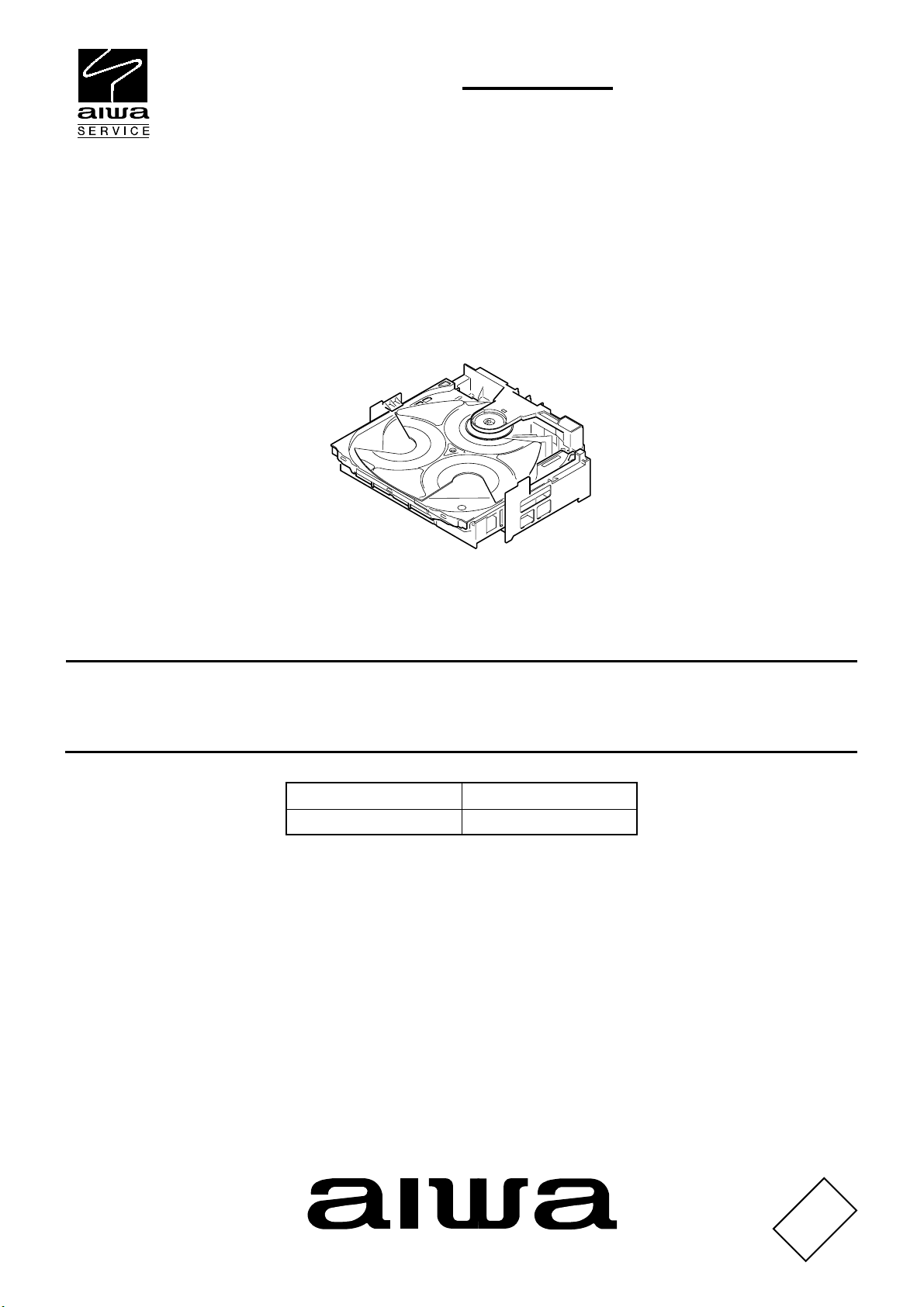
BZG-2
English
SIMPLE-2
SERVICE MANUAL
CD-R/RW MECHANISM
TYPE
ZD9NC
Apartofcontentsisadequate.
Re-issuing is under request.
BASIC CD MECHANISM : BZG-6ANC
BASIC CD MECHANISM
BZG-6 ANC
S/M Code No. 09-00C-353-2N4
DA T A
Page 2
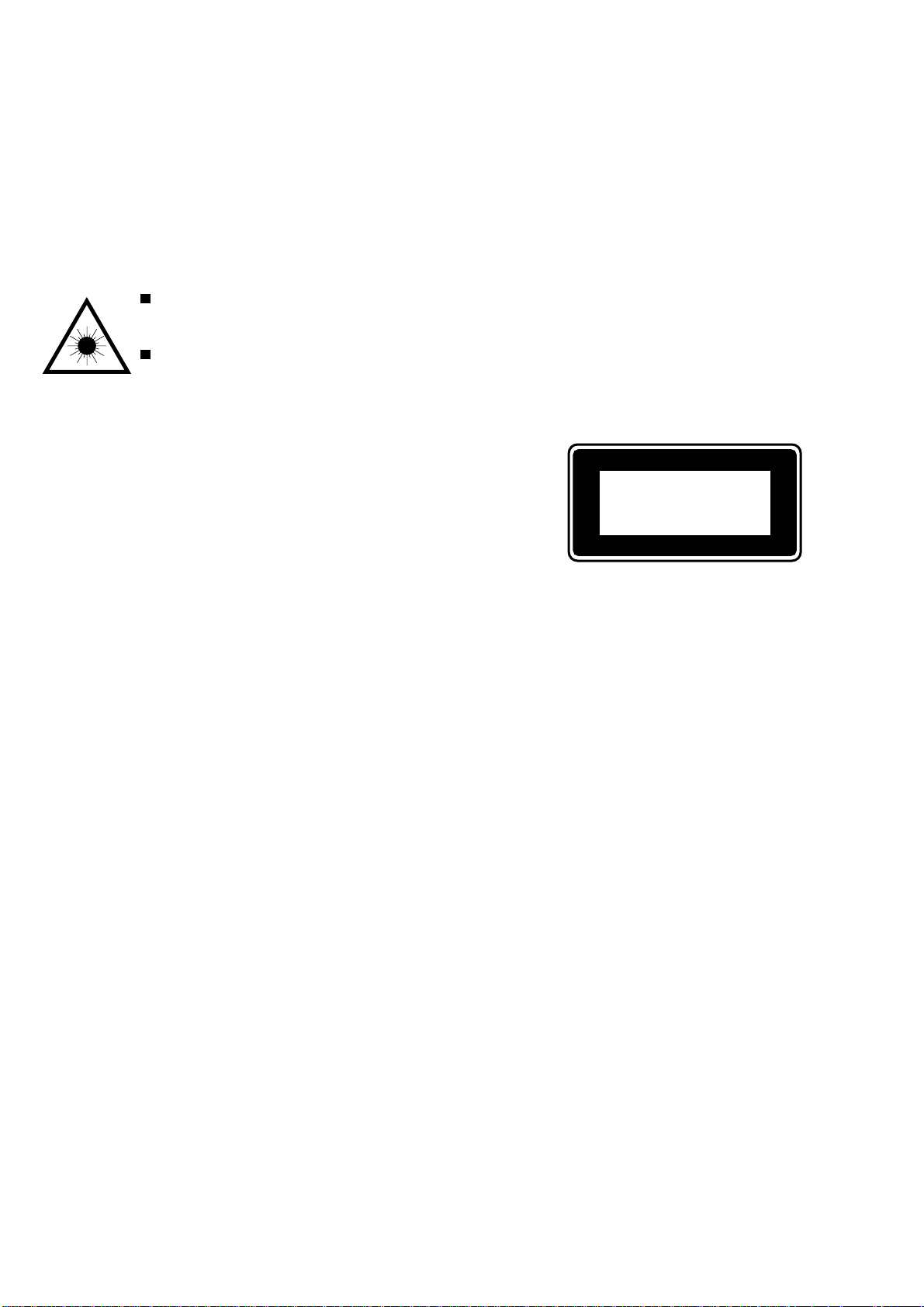
PROTECTION OF EYES FROM LASER BEAM DURING SERVICING
This set employs laser. Therefore, be sure to follow carefully the
instructions below when servicing.
WARNING!
WHEN SERVICING, DO NOT APPROACH THE LASER EXIT
WITH THE EYE TOO CLOSELY. IN CASE IT IS NECESSARY TO
CONFIRM LASER BEAM EMISSION. BE SURE TO OBSERVE
FROM A DISTANCE OF MORE THAN 30cm FROM THE
SURFACE OF THE OBJECTIVE LENS ON THE OPTICAL
PICK-UP BLOCK.
Caution: Invisible laser radiation when
open and interlocks defeated avoid exposure to beam.
Advarsel:Usynling laserståling ved åbning,
når sikkerhedsafbrydere er ude af funktion.
Undgå udsættelse for stråling.
VAROITUS!
Laiteen Käyttäminen muulla kuin tässä käyttöohjeessa mainitulla tavalla saattaa altistaa käyt-täjän turvallisuusluokan 1 ylittävälle näkymättömälle lasersäteilylle.
VARNING!
Om apparaten används på annat sätt än vad som specificeras i
denna bruksanvising, kan användaren utsättas för osynling
laserstrålning, som överskrider gränsen för laserklass 1.
CAUTION
Use of controls or adjustments or performance of procedures
other than those specified herein may result in hazardous
radiation exposure.
ATTENTION
L'utilisation de commandes, réglages ou procédures autres que
ceux spécifiés peut entraîner une dangereuse exposition aux
radiations.
ADVARSEL!
Usynlig laserståling ved åbning, når sikkerhedsafbrydereer ude
af funktion. Undgå udsættelse for stråling.
This Compact Disc player is classified as a CLASS 1 LASER
product.
The CLASS 1 LASER PRODUCT label is located on the rear
exterior.
CLASS 1
KLASSE 1
LUOKAN 1
KLASS 1
LASER PRODUCT
LASER PRODUKT
LASER LAITE
LASER APPARAT
-2-
Page 3

Precaution to replace Optical block
(PXR-104X-BP-0101)
Body or clothes electrostatic potential could ruin
laser diode in the optical block. Be sure ground
body and workbench, and use care the clothes
do not touch the diode.
1) After the connection, remove solder shown in
the right figure.
PICK-UP Assy PWB
Solder
-3-
Page 4
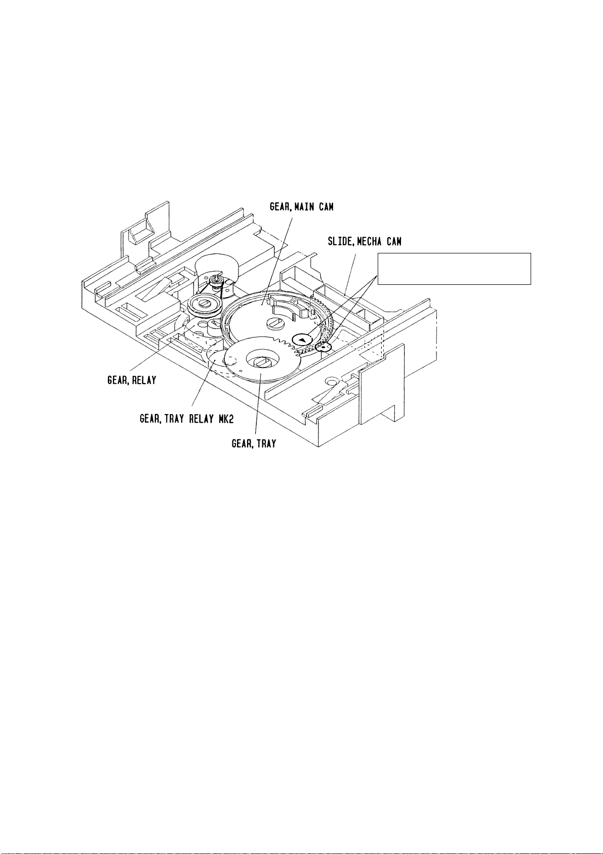
How to Adjust the Rotating Phase of the
Gear, Main Cam
1) Push down the hooking catch of the CHAS. MECH, and remove
the TRAY.
2) Align the arrow mark of the Gear, Main Cam with the black round
mark of the CHAS, MECHA as shown below.
3) Confirm that the Slide, Mech Cam is located in the right position,
then insert the TRAY gently.
Caution: If the rotating phase of the Gear, Main Cam is
incorrectly adjusted, the chucking operation and tray
movement will have malfunction.
Align the arrow 2 mark with the black
round • mark.
-4-
Page 5

ELECTRICAL PARTS LIST -1/7 (3CD C.B -1/5)
! = ! SAFTY PARTS
C = Components marked
UNIT-NAME ! C REF-NO PARTS-NO PARTS-NAME SUFFIX&MODEL
BZA-2
ZD9NC
3CD C.B O C 0001 87-010-759-080 C-CAP,U 0.1-25 Z F a
3CD C.B O C 0002 87-010-263-080 CAP,E 100-10 M 11L SME a
3CD C.B O C 0003 87-A10-915-080 C-CAP,U 1000P-25 J CH a
3CD C.B O C 0004 87-010-759-080 C-CAP,U 0.1-25 Z F a
3CD C.B O C 0005 87-010-263-080 CAP,E 100-10 M 11L SME a
3CD C.B O C 0006 87-010-405-080 CAP,E 10-50 M 11L SME a
3CD C.B O C 0101 87-A10-504-080 C-CAP,U 0.047-16 K B a
3CD C.B O C 0102 87-010-759-080 C-CAP,U 0.1-25 Z F a
3CD C.B O C 0103 87-012-195-080 C-CAP,U 100P-50 J CH a
3CD C.B O C 0104 87-012-282-080 C-CAP,U 4700P-50 K B a
3CD C.B O C 0105 87-010-759-080 C-CAP,U 0.1-25 Z F a
3CD C.B O C 0106 87-010-263-080 CAP,E 100-10 M 11L SME a
3CD C.B O C 0107 87-010-263-040 CAP,E 100-10 M 11L SME a
3CD C.B O C 0108 87-010-759-080 C-CAP,U 0.1-25 Z F a
3CD C.B O C 0109 87-010-263-040 CAP,E 100-10 M 11L SME a
3CD C.B O C 0110 87-010-405-040 CAP,E 10-50 M 11L SME a
3CD C.B O C 0111 87-010-401-080 CAP,E 1-50 M 11L SME a
3CD C.B O C 0114 87-012-188-080 C-CAP,U 47P-50 J CH a
3CD C.B O C 0115 87-010-759-080 C-CAP,U 0.1-25 Z F a
3CD C.B O C 0116 87-010-263-040 CAP,E 100-10 M 11L SME a
BZA-2
ZD9NC
3CD C.B O C 0117 87-010-263-080 CAP,E 100-10 M 11L SME a
3CD C.B O C 0118 87-010-759-080 C-CAP,U 0.1-25 Z F a
3CD C.B O C 0121 87-010-263-080 CAP,E 100-10 M 11L SME a
3CD C.B O C 0122 87-010-759-080 C-CAP,U 0.1-25 Z F a
3CD C.B O C 0123 87-012-169-080 C-CAP,U 7P-50 D CH a
3CD C.B O C 0124 87-012-172-080 C-CAP,U 10P-50 D CH a
3CD C.B O C 0126 87-010-403-080 CAP,E 3.3-50 M 11L SME a
3CD C.B O C 0127 87-010-759-080 C-CAP,U 0.1-25 Z F a
3CD C.B O C 0128 87-A10-504-080 C-CAP,U 0.047-16 K B a
3CD C.B O C 0129 87-010-403-040 CAP,E 3.3-50 M 11L SME a
3CD C.B O C 0130 87-010-759-080 C-CAP,U 0.1-25 Z F a
3CD C.B O C 0131 87-010-759-080 C-CAP,U 0.1-25 Z F a
3CD C.B O C 0132 87-010-263-040 CAP,E 100-10 M 11L SME a
3CD C.B O C 0133 87-010-405-080 CAP,E 10-50 M 11L SME a
3CD C.B O C 0134 87-010-759-080 C-CAP,U 0.1-25 Z F a
3CD C.B O C 0135 87-010-260-080 CAP,E 47-25 M 11L SME a
3CD C.B O C 0136 87-010-759-080 C-CAP,U 0.1-25 Z F a
3CD C.B O C 0137 87-A10-915-080 C-CAP,U 1000P-25 J CH a
3CD C.B O C 0138 87-010-759-080 C-CAP,U 0.1-25 Z F a
3CD C.B O C 0160 87-016-669-080 C-CAP,S 0.1-25 K B a
BZA-2
ZD9NC
3CD C.B O C 0161 87-A10-826-080 C-CAP,S 1-10 K B a
3CD C.B O C 0203 87-010-112-080 CAP,E 100-16 M 11L SME a
3CD C.B O C 0204 87-010-759-080 C-CAP,U 0.1-25 Z F a
3CD C.B O C 0205 87-010-263-040 CAP,E 100-10 M 11L SME a
3CD C.B O C 0208 87-010-759-080 C-CAP,U 0.1-25 Z F a
3CD C.B O C 0212 87-010-405-040 CAP,E 10-50 M 11L SME a
3CD C.B O C 0213 87-010-759-080 C-CAP,U 0.1-25 Z F a
3CD C.B O C 0214 87-010-759-080 C-CAP,U 0.1-25 Z F a
3CD C.B O C 0301 87-010-382-080 CAP,E 22-25 M 11L SME a
3CD C.B O C 0302 87-010-759-080 C-CAP,U 0.1-25 Z F a
3CD C.B O C 0303 87-010-260-080 CAP,E 47-25 M 11L SME a
3CD C.B O C 0304 87-010-759-080 C-CAP,U 0.1-25 Z F a
3CD C.B O C 0305 87-A10-915-080 C-CAP,U 1000P-25 J CH a
3CD C.B O C 0401 87-012-195-080 C-CAP,U 100P-50 J CH a
3CD C.B O C 0402 87-012-195-080 C-CAP,U 100P-50 J CH a
3CD C.B O C 0403 87-012-195-080 C-CAP,U 100P-50 J CH a
3CD C.B O C 0404 87-012-195-080 C-CAP,U 100P-50 J CH a
3CD C.B O C 0405 87-012-195-080 C-CAP,U 100P-50 J CH a
3CD C.B O CN 0001 87-A60-429-010 CONN,16P H TOC-A a
3CD C.B O CN 0201 87-099-199-010 CONN,6P H BLK 6216 a
All components used on this model at the production line are shown in this service manual.
However, please note that not all components will be available as spare parts for after-sales service.
Components marked S and O are designated as spare parts for service and will be stocked at the spare parts centers.
Components marked X and R are not designated as spare parts for after sales service, and will not be stocked at the spare parts centers.
-5-
Page 6

ELECTRICAL PARTS LIST -2/7 (3CD C.B -2/5)
! = ! SAFTY PARTS
C = Components marked
UNIT-NAME ! C REF-NO PARTS-NO PARTS-NAME SUFFIX&MODEL
BZA-2
ZD9NC
3CD C.B O CN 0202 87-A60-130-010 CONN,5P V FE a
3CD C.B O CN 0301 87-A60-154-010 CONN,6P H FE a
3CD C.B O CN 0401 87-099-201-010 CONN,8P H BLK 6216 a
3CD C.B S D 0101 87-A40-743-080 ZENER,UZ4.3BSA a
3CD C.B S D 0102 87-A40-747-080 ZENER,UZ5.1BSB a
3CD C.B S D 0103 87-A40-270-080 C-DIODE,MC2838 a
3CD C.B S D 0301 87-A40-753-080 ZENER,UZ6.8BSB a
3CD C.B S D 0303 87-020-465-080 DIODE,1SS133 a
3CD C.B S D 0304 87-020-465-080 DIODE,1SS133 a
3CD C.B S IC 0101 87-A21-821-130 C-IC,LC78645NE a
3CD C.B S IC 0201 87-A21-414-010 IC,BA5927S a
3CD C.B X JR 0121 88-129-000-080 C-JUMPER, 3216 a
3CD C.B X JR 0201 88-108-000-080 C-JUMPER,U a
3CD C.B X JR 0202 88-108-000-080 C-JUMPER,U a
3CD C.B X JR 0203 88-108-000-080 C-JUMPER,U a
3CD C.B X JR 0204 88-108-000-080 C-JUMPER,U a
3CD C.B X JR 0401 88-129-000-080 C-JUMPER, 3216 a
3CD C.B X JR 0402 88-129-000-080 C-JUMPER, 3216 a
3CD C.B X JR 0403 88-108-000-080 C-JUMPER,U a
3CD C.B X JW 0001 88-100-000-010 PLATING-JW, 0.58 SN95 a
BZA-2
ZD9NC
3CD C.B X JW 0002 88-100-000-010 PLATING-JW, 0.58 SN95 a
3CD C.B X JW 0004 88-100-000-010 PLATING-JW, 0.58 SN95 a
3CD C.B X JW 0005 88-100-000-010 PLATING-JW, 0.58 SN95 a
3CD C.B X JW 0006 88-100-000-010 PLATING-JW, 0.58 SN95 a
3CD C.B X JW 0007 88-100-000-010 PLATING-JW, 0.58 SN95 a
3CD C.B X JW 0008 88-100-000-010 PLATING-JW, 0.58 SN95 a
3CD C.B X JW 0009 88-100-000-010 PLATING-JW, 0.58 SN95 a
3CD C.B X JW 0101 88-100-000-010 PLATING-JW, 0.58 SN95 a
3CD C.B X JW 0102 88-100-000-010 PLATING-JW, 0.58 SN95 a
3CD C.B X JW 0103 88-100-000-010 PLATING-JW, 0.58 SN95 a
3CD C.B X JW 0104 88-100-000-010 PLATING-JW, 0.58 SN95 a
3CD C.B X JW 0105 88-100-000-010 PLATING-JW, 0.58 SN95 a
3CD C.B X JW 0106 88-100-000-010 PLATING-JW, 0.58 SN95 a
3CD C.B X JW 0107 88-100-000-010 PLATING-JW, 0.58 SN95 a
3CD C.B X JW 0108 88-100-000-010 PLATING-JW, 0.58 SN95 a
3CD C.B X JW 0109 88-100-000-010 PLATING-JW, 0.58 SN95 a
3CD C.B X JW 0110 88-100-000-010 PLATING-JW, 0.58 SN95 a
3CD C.B X JW 0112 88-100-000-010 PLATING-JW, 0.58 SN95 a
3CD C.B X JW 0113 88-100-000-010 PLATING-JW, 0.58 SN95 a
3CD C.B X JW 0114 88-100-000-010 PLATING-JW, 0.58 SN95 a
BZA-2
ZD9NC
3CD C.B X JW 0115 88-100-000-010 PLATING-JW, 0.58 SN95 a
3CD C.B X JW 0116 88-100-000-010 PLATING-JW, 0.58 SN95 a
3CD C.B X JW 0117 88-100-000-010 PLATING-JW, 0.58 SN95 a
3CD C.B X JW 0121 88-100-000-010 PLATING-JW, 0.58 SN95 a
3CD C.B X JW 0124 88-100-000-010 PLATING-JW, 0.58 SN95 a
3CD C.B X JW 0125 88-100-000-010 PLATING-JW, 0.58 SN95 a
3CD C.B X JW 0126 88-100-000-010 PLATING-JW, 0.58 SN95 a
3CD C.B X JW 0131 88-100-000-010 PLATING-JW, 0.58 SN95 a
3CD C.B X JW 0133 88-100-000-010 PLATING-JW, 0.58 SN95 a
3CD C.B X JW 0134 88-100-000-010 PLATING-JW, 0.58 SN95 a
3CD C.B X JW 0151 88-100-000-010 PLATING-JW, 0.58 SN95 a
3CD C.B X JW 0152 88-100-000-010 PLATING-JW, 0.58 SN95 a
3CD C.B X JW 0153 88-100-000-010 PLATING-JW, 0.58 SN95 a
3CD C.B X JW 0201 88-100-000-010 PLATING-JW, 0.58 SN95 a
3CD C.B X JW 0202 88-100-000-010 PLATING-JW, 0.58 SN95 a
3CD C.B X JW 0203 88-100-000-010 PLATING-JW, 0.58 SN95 a
3CD C.B X JW 0204 88-100-000-010 PLATING-JW, 0.58 SN95 a
3CD C.B X JW 0205 88-100-000-010 PLATING-JW, 0.58 SN95 a
3CD C.B X JW 0206 88-100-000-010 PLATING-JW, 0.58 SN95 a
3CD C.B X JW 0207 88-100-000-010 PLATING-JW, 0.58 SN95 a
All components used on this model at the production line are shown in this service manual.
However, please note that not all components will be available as spare parts for after-sales service.
Components marked S and O are designated as spare parts for service and will be stocked at the spare parts centers.
Components marked X and R are not designated as spare parts for after sales service, and will not be stocked at the spare parts centers.
-6-
Page 7

ELECTRICAL PARTS LIST -3/7 (3CD C.B -3/5)
! = ! SAFTY PARTS
C = Components marked
UNIT-NAME ! C REF-NO PARTS-NO PARTS-NAME SUFFIX&MODEL
BZA-2
ZD9NC
3CD C.B X JW 0210 88-100-000-010 PLATING-JW, 0.58 SN95 a
3CD C.B X JW 0211 88-100-000-010 PLATING-JW, 0.58 SN95 a
3CD C.B X JW 0212 88-100-000-010 PLATING-JW, 0.58 SN95 a
3CD C.B X JW 0213 88-100-000-010 PLATING-JW, 0.58 SN95 a
3CD C.B X JW 0214 88-100-000-010 PLATING-JW, 0.58 SN95 a
3CD C.B X JW 0215 88-100-000-010 PLATING-JW, 0.58 SN95 a
3CD C.B X JW 0217 88-100-000-010 PLATING-JW, 0.58 SN95 a
3CD C.B X JW 0218 88-100-000-010 PLATING-JW, 0.58 SN95 a
3CD C.B X JW 0219 88-100-000-010 PLATING-JW, 0.58 SN95 a
3CD C.B X JW 0220 88-100-000-010 PLATING-JW, 0.58 SN95 a
3CD C.B X JW 0221 88-100-000-010 PLATING-JW, 0.58 SN95 a
3CD C.B X JW 0222 88-100-000-010 PLATING-JW, 0.58 SN95 a
3CD C.B X JW 0223 88-100-000-010 PLATING-JW, 0.58 SN95 a
3CD C.B X JW 0224 88-100-000-010 PLATING-JW, 0.58 SN95 a
3CD C.B X JW 0225 88-100-000-010 PLATING-JW, 0.58 SN95 a
3CD C.B X JW 0226 88-100-000-010 PLATING-JW, 0.58 SN95 a
3CD C.B X JW 0227 88-100-000-010 PLATING-JW, 0.58 SN95 a
3CD C.B X JW 0228 88-100-000-010 PLATING-JW, 0.58 SN95 a
3CD C.B X JW 0229 88-100-000-010 PLATING-JW, 0.58 SN95 a
3CD C.B X JW 0230 88-100-000-010 PLATING-JW, 0.58 SN95 a
BZA-2
ZD9NC
3CD C.B X JW 0231 88-100-000-010 PLATING-JW, 0.58 SN95 a
3CD C.B X JW 0232 88-100-000-010 PLATING-JW, 0.58 SN95 a
3CD C.B X JW 0234 88-100-000-010 PLATING-JW, 0.58 SN95 a
3CD C.B X JW 0236 88-100-000-010 PLATING-JW, 0.58 SN95 a
3CD C.B X JW 0237 88-100-000-010 PLATING-JW, 0.58 SN95 a
3CD C.B X JW 0301 88-100-000-010 PLATING-JW, 0.58 SN95 a
3CD C.B X JW 0302 88-100-000-010 PLATING-JW, 0.58 SN95 a
3CD C.B X JW 0303 88-100-000-010 PLATING-JW, 0.58 SN95 a
3CD C.B X JW 0304 88-100-000-010 PLATING-JW, 0.58 SN95 a
3CD C.B X JW 0305 88-100-000-010 PLATING-JW, 0.58 SN95 a
3CD C.B X JW 0306 88-100-000-010 PLATING-JW, 0.58 SN95 a
3CD C.B X JW 0401 88-100-000-010 PLATING-JW, 0.58 SN95 a
3CD C.B O L 0101 87-005-469-080 COIL,4.7UH J FLR50 a
3CD C.B S Q 0001 87-026-609-080 TR,KTA1266GR a
3CD C.B S Q 0101 87-026-610-080 TR,KTC3198GR a
3CD C.B S Q 0102 87-A30-073-080 C-TR,RT1N 141C a
3CD C.B S Q 0210 87-026-609-080 TR,KTA1266GR a
3CD C.B S Q 0301 87-A30-076-080 C-TR,2SC3052F a
3CD C.B S Q 0302 87-A30-515-080 TR,2SA1979O/Y a
3CD C.B S Q 0303 87-A30-515-080 TR,2SA1979O/Y a
BZA-2
ZD9NC
3CD C.B S Q 0304 87-A30-515-080 TR,2SA1979O/Y a
3CD C.B S Q 0305 87-A30-515-080 TR,2SA1979O/Y a
3CD C.B S Q 0306 87-A30-515-080 TR,2SA1979O/Y a
3CD C.B X R 0001 88-108-333-080 C-RES,U 33K-1/16W J a
3CD C.B X R 0002 88-108-153-080 C-RES,U 15K-1/16W J a
3CD C.B X R 0003 88-108-153-080 C-RES,U 15K-1/16W J a
3CD C.B X R 0004 88-108-153-080 C-RES,U 15K-1/16W J a
3CD C.B X R 0005 88-108-153-080 C-RES,U 15K-1/16W J a
3CD C.B X R 0006 88-108-333-080 C-RES,U 33K-1/16W J a
3CD C.B X R 0007 88-108-181-080 C-RES,U 180-1/16W J a
3CD C.B X R 0008 88-108-339-080 C-RES,U 3.3-1/16W J a
3CD C.B X R 0010 88-129-000-080 C-JUMPER, 3216 a
3CD C.B X R 0101 88-108-103-080 C-RES,U 10K-1/16W J a
3CD C.B X R 0102 88-108-273-080 C-RES,U 27K-1/16W J a
3CD C.B X R 0103 88-108-331-080 C-RES,U 330-1/16W J a
3CD C.B O R 0104 87-012-278-080 C-CAP,U 2200P-50 K B a
3CD C.B X R 0105 88-108-000-080 C-JUMPER,U a
3CD C.B O R 0106 87-012-274-080 C-CAP,U 1000P-50 K B a
3CD C.B X R 0107 88-108-000-080 C-JUMPER,U a
3CD C.B X R 0108 88-118-000-080 C-JUMPER,S a
All components used on this model at the production line are shown in this service manual.
However, please note that not all components will be available as spare parts for after-sales service.
Components marked S and O are designated as spare parts for service and will be stocked at the spare parts centers.
Components marked X and R are not designated as spare parts for after sales service, and will not be stocked at the spare parts centers.
-7-
Page 8

ELECTRICAL PARTS LIST -4/7 (3CD C.B -4/5)
! = ! SAFTY PARTS
C = Components marked
UNIT-NAME ! C REF-NO PARTS-NO PARTS-NAME SUFFIX&MODEL
BZA-2
ZD9NC
3CD C.B X R 0110 88-108-221-080 C-RES,U 220-1/16W J a
3CD C.B X R 0111 88-108-470-080 C-RES,U 47-1/16W J a
3CD C.B X R 0112 88-108-102-080 C-RES,U 1K-1/16W J a
3CD C.B X R 0113 88-108-102-080 C-RES,U 1K-1/16W J a
3CD C.B X R 0114 88-108-102-080 C-RES,U 1K-1/16W J a
3CD C.B X R 0115 88-108-102-080 C-RES,U 1K-1/16W J a
3CD C.B X R 0116 88-108-102-080 C-RES,U 1K-1/16W J a
3CD C.B X R 0117 88-108-102-080 C-RES,U 1K-1/16W J a
3CD C.B X R 0118 88-108-224-080 C-RES,U 220K-1/16W J a
3CD C.B X R 0119 88-108-681-080 C-RES,U 680-1/16W J a
3CD C.B X R 0120 88-108-681-080 C-RES,U 680-1/16W J a
3CD C.B X R 0121 88-108-123-080 C-RES,U 12K-1/16W J a
3CD C.B X R 0122 88-108-122-080 C-RES,U 1.2K-1/16W J a
3CD C.B X R 0123 88-118-152-080 C-RES,S 1.5K-1/10W J a
3CD C.B X R 0124 88-118-152-080 C-RES,S 1.5K-1/10W J a
3CD C.B X R 0125 88-118-102-080 C-RES,S 1K-1/10W J a
3CD C.B X R 0126 88-118-101-080 C-RES,S 100-1/10W J a
3CD C.B X R 0127 88-118-100-080 C-RES,S 10-1/10W J a
3CD C.B X R 0128 88-100-000-010 PLATING-JW, 0.58 SN95 a
3CD C.B X R 0129 88-129-000-080 C-JUMPER, 3216 a
BZA-2
ZD9NC
3CD C.B X R 0130 88-108-103-080 C-RES,U 10K-1/16W J a
3CD C.B X R 0131 88-108-473-080 C-RES,U 47K-1/16W J a
3CD C.B X R 0132 88-118-470-080 C-RES,S 47-1/10W J a
3CD C.B X R 0133 88-118-152-080 C-RES,S 1.5K-1/10W J a
3CD C.B X R 0134 88-118-152-080 C-RES,S 1.5K-1/10W J a
3CD C.B X R 0137 88-108-102-080 C-RES,U 1K-1/16W J a
3CD C.B X R 0138 88-108-102-080 C-RES,U 1K-1/16W J a
3CD C.B X R 0151 88-108-101-080 C-RES,U 100-1/16W J a
3CD C.B X R 0152 88-108-101-080 C-RES,U 100-1/16W J a
3CD C.B X R 0160 88-108-103-080 C-RES,U 10K-1/16W J a
3CD C.B X R 0161 88-121-153-080 RES,15K-1/8W J a
3CD C.B X R 0203 88-108-473-080 C-RES,U 47K-1/16W J a
3CD C.B X R 0209 88-108-472-080 C-RES,U 4.7K-1/16W J a
3CD C.B X R 0212 88-108-182-080 C-RES,U 1.8K-1/16W J a
3CD C.B X R 0213 88-108-392-080 C-RES,U 3.9K-1/16W J a
3CD C.B X R 0216 88-108-273-080 C-RES,U 27K-1/16W J a
3CD C.B X R 0219 88-108-273-080 C-RES,U 27K-1/16W J a
3CD C.B X R 0220 88-108-103-080 C-RES,U 10K-1/16W J a
3CD C.B X R 0221 88-108-822-080 C-RES,U 8.2K-1/16W J a
3CD C.B X R 0222 88-108-562-080 C-RES,U 5.6K-1/16W J a
BZA-2
ZD9NC
3CD C.B X R 0223 88-108-562-080 C-RES,U 5.6K-1/16W J a
3CD C.B X R 0225 88-108-123-080 C-RES,U 12K-1/16W J a
3CD C.B X R 0226 88-108-123-080 C-RES,U 12K-1/16W J a
3CD C.B X R 0227 88-108-123-080 C-RES,U 12K-1/16W J a
3CD C.B X R 0228 88-108-103-080 C-RES,U 10K-1/16W J a
3CD C.B X R 0229 88-118-339-080 C-RES,S 3.3-1/10W J a
3CD C.B X R 0230 88-118-101-080 C-RES,S 100-1/10W J a
3CD C.B X R 0231 88-118-101-080 C-RES,S 100-1/10W J a
3CD C.B X R 0233 88-121-221-080 RES,220-1/8W J a
3CD C.B X R 0301 88-128-102-080 C-RES, 1K-1/8W J a
3CD C.B X R 0302 88-118-101-080 C-RES,S 100-1/10W J a
3CD C.B X R 0303 88-118-561-080 C-RES,S 560-1/10W J a
3CD C.B X R 0304 88-118-392-080 C-RES,S 3.9K-1/10W J a
3CD C.B X R 0305 88-128-100-080 C-RES, 10-1/8W J a
3CD C.B X R 0306 88-128-100-080 C-RES, 10-1/8W J a
3CD C.B X R 0307 88-128-100-080 C-RES, 10-1/8W J a
3CD C.B X R 0308 88-128-100-080 C-RES, 10-1/8W J a
3CD C.B X R 0309 88-128-100-080 C-RES, 10-1/8W J a
3CD C.B X R 0310 88-128-109-080 C-RES, 1-1/8W J a
3CD C.B X R 0311 88-128-109-080 C-RES, 1-1/8W J a
All components used on this model at the production line are shown in this service manual.
However, please note that not all components will be available as spare parts for after-sales service.
Components marked S and O are designated as spare parts for service and will be stocked at the spare parts centers.
Components marked X and R are not designated as spare parts for after sales service, and will not be stocked at the spare parts centers.
-8-
Page 9

ELECTRICAL PARTS LIST -5/7 (3CD C.B -5/5)
! = ! SAFTY PARTS
C = Components marked
UNIT-NAME ! C REF-NO PARTS-NO PARTS-NAME SUFFIX&MODEL
BZA-2
ZD9NC
3CD C.B X R 0312 88-128-109-080 C-RES, 1-1/8W J a
3CD C.B X R 0313 88-128-109-080 C-RES, 1-1/8W J a
3CD C.B X R 0314 88-128-109-080 C-RES, 1-1/8W J a
3CD C.B X R 0401 88-108-101-080 C-RES,U 100-1/16W J a
3CD C.B X R 0402 88-108-101-080 C-RES,U 100-1/16W J a
3CD C.B X R 0403 88-108-101-080 C-RES,U 100-1/16W J a
3CD C.B X R 0404 88-108-101-080 C-RES,U 100-1/16W J a
3CD C.B X R 0405 88-108-101-080 C-RES,U 100-1/16W J a
3CD C.B X R 0406 88-108-101-080 C-RES,U 100-1/16W J a
3CD C.B X R 0407 88-108-101-080 C-RES,U 100-1/16W J a
3CD C.B X R 0408 88-108-101-080 C-RES,U 100-1/16W J a
3CD C.B X R 0415 88-108-182-080 C-RES,U 1.8K-1/16W J a
3CD C.B X R 0416 88-121-122-080 RES,1.2K-1/8W J a
3CD C.B X R 0417 88-108-562-080 C-RES,U 5.6K-1/16W J a
3CD C.B O S 0401 87-036-109-010 SW,MICRO SPPB61 a
3CD C.B O S 0402 87-036-109-010 SW,MICRO SPPB61 a
3CD C.B O X 0101 87-A70-318-010 VIB,XTAL 33.8688MHZ CSA-309 a
All components used on this model at the production line are shown in this service manual.
However, please note that not all components will be available as spare parts for after-sales service.
Components marked S and O are designated as spare parts for service and will be stocked at the spare parts centers.
Components marked X and R are not designated as spare parts for after sales service, and will not be stocked at the spare parts centers.
-9-
Page 10

ELECTRICAL PARTS LIST -6/7 (T-T C.B/MOTOR C.B -1/1)
! = ! SAFTY PARTS
C = Components marked
UNIT-NAME ! C REF-NO PARTS-NO PARTS-NAME SUFFIX&MODEL
BZG-2
ZD9NC
MOTOR C.B O CN 0001 87-A60-086-010 CONN,06P H 6216 a
MOTOR C.B O M 0001 87-045-358-010 MOT,RF-310TA 43 a
MOTOR C.B O M 0002 87-045-363-010 MOT,MDN4RA3ETA1 a
MOTOR C.B O SW 0001 87-A90-042-010 SW,LEAF MSW-17310MVP0 a
T-T C.B O C 0401 87-A11-148-080 CAP,TC U 0.1-50 Z F a
T-T C.B O CN 0401 86-NFZ-675-010 CONN,5P H 6216-11H a
T-T C.B O PS 0401 87-A90-156-010 SNSR,SG-240 a
T-T C.B X R 0408 88-121-561-080 RES,560-1/8W J a
T-T C.B X R 0409 88-121-273-080 RES,27K-1/8W J a
All components used on this model at the production line are shown in this service manual.
However, please note that not all components will be available as spare parts for after-sales service.
Components marked S and O are designated as spare parts for service and will be stocked at the spare parts centers.
Components marked X and R are not designated as spare parts for after sales service, and will not be stocked at the spare parts centers.
-10-
Page 11

ELECTRICAL PARTS LIST-7/7
• Regarding connectors, they are not stocked as they are not the initial order items.
The connectors are available after they are supplied from connector manufacturers upon the order is received.
CHIP RESISTOR PART CODE
Chip Resistor Part Coding
88
A
Resistor Code
Chip resistor
Wattage Type Tolerance
1/16W 1005 5% CJ
1/16W
1/10W
1/8W
1608
2125
3216
5%
5%
5%
Symbol
CJ
CJ
CJ
Figure
Value of resistor
Form
L
Dimensions (mm)
t
W
0.55
Resistor Code
108
118
128
LW t
1.0 0.5 0.35 104
1.6 0.8 0.45
2 1.25 0.45
3.2
1.6
: A
: A
-11-
Page 12

TRANSISTOR ILLUSTRATION-1/1
C
B
E
ECB
ECB
2SC3052F
RT1N 141C
2SA19790/Y
KTA1266GR
KTC3198GR
-12-
Page 13

BLOCK DIAGRAM-1/1
BZG-6 ANC
3CD
TRAY
CD MOUNT
PXR-104X-BP-0101
-13-
Page 14

WIRING-1/2 (MAIN)
101112131415161718192021222324
1234567892526272829303132
A
(TRAY SW)
3CD C.B
MOTOR
(CD MOUNT
SW)
B
PX-104X-BP-0101
C
D
E
F
G
H
I
J
K
L
M
N
O
P
Q
R
S
-14-
U
T
U
Page 15

SCHEMATIC DIAGRAM-1/1
3CD
BZG-6 ANC
SPPB61
CD MOUNT SW
OFF UP
ON ª
OFF DOWN
SPPB61
TRAY SW
ON OPEN
OFF CLOSE
ª
PXR-104X-BP-0101
-15-
Page 16

WIRING-2/2 (T-T/MOTOR)
123456789101112131415
A
B
C
D
E
F
G
H
MOTOR C.B
M1
SW1
M2
(BZG6 ANC)
M1
SPINDLE
MOTOR
SW1
(LIMIT SW)
I
J
K
L
M
N
O
P
Q
CN1
3CD C.B
CNA203
R
M2
SLED
MOTOR
16
S
T
U
-16-
Page 17

WAVE FORM-1/1
1 IC201 ⁄ (OUT6-) VOLT/DIV: 500mV
TIME/DIV: 200mS
2 IC201 º (OUT6+)
1.6Vp-p
1.6Vp-p
3 Between CN202 1 and 2 VOLT/DIV: 1V
(2 Pin: 0 Level) TIME/DIV: 200mS
0
6 IC101 (RES) VOLT/DIV: 1V
7 IC101 (VDD5)
66
68
TIME/DIV: 10mS
8 IC101 ? (XOUT)
(POWER ON)
6Vp-p
6 IC101 (RES) VOLT/DIV: 1V
7 IC101 (VDD5)
66
68
5.2Vp-p
1.2Vp-p
TIME/DIV: 10mS
8 IC101 ? (XOUT)
(POWER OFF)
4 IC101 # (FE) VOLT/DIV: 500mV
TIME/DIV: 5mS
1.45Vp-p
5 IC101 % (TE) VOLT/DIV: 200mV
TIME/DIV: 200µS
1.24Vp-p
4.4Vp-p
5Vp-p
0Vp-p
-17-
Page 18

IC BLOCK DIAGRAM-1/1
IC, BA5927S
DETECTION
OF REG-OUT
CURRENT
-18-
Page 19

IC DESCRIPTION-1/1 (LC78645)-1/3
Pin No. Pin Name I/O Description
1
2
3
SLCO
SLCIST
EFMIN
O
I
Slice level control SLCO output current adjustment resistor connection pin.
I
Control output.
RF signal input pin.
10
11
12
13
14
15
16
17
18
19
20
21
22
4
5
6
7
8
9
RF
RFVDD
RFVSS
FIN1
FIN2
TIN1
TIN2
VREF
REFI
EF
TEC
TE
RFMON
JITTC
ADAVDD
ADAVSS
TDO
FDO
SPDO
—
—
—
—
O
RF monitor pin.
RF power supply pin.
RF ground pin. Must be connected to 0V.
I
A+C signal input pin.
I
B+D signal input pin.
I
E signal input pin.
I
F signal input pin.
O
VREF voltage output pin.
I
Reference voltage output setting pin.
O
FE signal monitor pin.
O
TE signal LPF capacitor connection pin.
O
TE signal monitor pin.
O
RF internal signal monitor pin.
O
Jitter detection capacitor connection pin.
Servo A/D, D/A supply pin.
Servo A/D, D/A ground pin. Must be connected to 0V.
O
Tracking control output pin. D/A output.
O
Focus control output pin. D/A output.
O
Spindle control output pin. D/A output.
23
24
25, 26
27
28
29
30
31
32-36
37
38
39
40
SLDO
GPDAC
CONT4, 5
SBCK/CONT6
SBCK/FG
DEFECT
V/P
FSEQ
MONI1, 5
VSS
VDD
DOUT
TEST
O
O
I/O
I/O
O
O
O
O
—
—
O
Thread control output pin. D/A output.
Servo D/A general-purpose output pin. (Not connected)
General-purpose input/output pin 4, 5. Controlled by commands from the microprocessor.
General-purpose input/output pin 6,
or subcode read clock input pin.
Subcode read clock input pin/FG signal input pin/external emphasis setting pin.
I
Set to command -pin function. Must be connected to 0V.
Defect pin. (Not connected)
Rouge servo/phase control automatic switching monitor output pin.
“H” for rough servo and “L” for phase servo. (Not connected)
Synchronization signal detection output pin.
Outputs a high level when the synchronization signal detected from the EFM signal and the
internally generated synchronization signal agree. (Not connected)
Internal signal monitor pin 1, 5. (Not connected)
Digital ground pin. Must be connected to 0V.
Digital power supply pin.
Digital OUT output pin. (Not connected)
I
Test input pin. Must be connected to 0V.
Any of these that are unused must be either set up as
input pin ports and connected to 0V, or set up as
output pin ports and left open.
-19-
Page 20

IC DESCRIPTION-1/1 (LC78645)-2/3
Pin No. Pin Name I/O Description
41
42
43
LVDD
LCHO
LVSS
—
—
Lchannel power supply pin.
O
L channel D/A converter L channel output pin.
L channel ground pin. Must be connected to 0V.
44
45
46
47
48
49
50
51
52
53
54
55
56
57
58
59
RVSS
RCHO
RVDD
XVDD
XOUT
XIN
FSX/16MIN
XVSS
C2F
EFLG
16MOUT
ASLRCK
ASDACK
ASDFIN
LRSY
DATACK
—
O
—
—
O
I/O
—
O
O
O
O
O
R channel ground pin. Must be connected to 0V.
R channel D/A converter R channel output pin.
R channel power supply pin.
Crystal oscillator
I
7.35kHz synchronization signal output pin.
DF, DAC external clock input pin. (Not connected)
Crystal oscillator
C2 flag output pin. (Not connected)
C1, C2 error correction monitor pin. (Not connected)
16.9344MHz output pin. (Not connected)
I
I
Antishock mode
I
Digital data output Bit clock output pin. (Not connected)
Crystal oscillator power supply pin.
Connection for a 33.8688MHz crystal oscillator pin.
Crystal oscillator ground pin.
Must be connected to 0V.
L/R clock input pin. Must be connected to 0V when unused.
Bit clock input pin. Must be connected to 0V when unused.
L/R channel data input pin. Must be connected to 0V when
unused.
L/R clock output pin. (Not connected)
60
61
62
63
64
65
66
67
68
69
70
71, 72
DATA
CE
CL
DI
DO
WRQ
RES
DRF
VDD5
VSS
CONT3
CONT2, 1
O
O
O
O
—
—
I/O
I/O
L/R channel data output pin. (Not connected)
I
I
I
Microprocessor interface Data input pin.
Reset input pin.
I
This pin must be set low briefly after power is first applied.
Focus ON detect pin.
Microprocessor interface power supply pin.
Digital ground pin. Must be connected to 0V.
General-purpose output pin 3. (Not connected) Controlled by commands from the
General-purpose output pin 2, 1.
Chip enable signal input pin.
Data transfer clock input pin.
Data output pin. (Nch open drain output)
Interruption signal output pin.
microprocessor .
Must be set as an input pin and connected to
0V or set as an output pin and left open
when unused.
-20-
Page 21

IC DESCRIPTION-1/1 (LC78645)-3/3
Pin No. Pin Name I/O Description
73, 74
75
76
PD01, 2
VVSS
PCKIST
—
O
I
PLL Resistor connection pin to set current for PD01 and 02 outputs.
Phase comparison output pin 1, 2 to control built-in VCO.
Built -in VCO GND pin. Must always be connected to 0V.
77
78
79
80
VVDD
FR
LDS
LDD
—
Built-in VCO power supply pin.
I
I
Laser power detection signal input pin.
O
Laser power control signal output pin.
Resistor connection pin to set the frequency range of built-in VCO.
-21-
Page 22

MECHANICAL EXPLODED VIEW-1/1
7
30
8
10
24
22
B
9
C
SH,25-40-0.5 PC
18
19
23
21
20
25
26
27
13
11
PWB
BZG-6
16
28
17
4
6
5
3
2
1
3
12
PWB
(BZA-2)
28
29
A
28
28
14
15
-22-
Page 23

MECANICAL PARTS LIST -1/1
! = ! SAFTY PARTS
C = Components marked
UNIT-NAME ! C REF-NO PARTS-NO PARTS-NAME SUFFIX&MODEL
BZG-2
ZD9NC
CD TRANSPORT O 1 8B-ZG2-602-010 FF-CABLE,5P 1.25 185MM a
CD TRANSPORT O 2 87-A91-982-010 MOT,M25E-4 2054 a
CD TRANSPORT O 3 84-ZG1-267-010 PULLEY,LOAD MO 8 a
CD TRANSPORT O 4 8B-ZG2-246-010 BELT,SQ 1-99.5 a
CD TRANSPORT O 5 8B-ZG2-241-110 GEAR,WORM a
CD TRANSPORT O 6 8B-ZG2-236-010 PULLEY,WORM a
CD TRANSPORT O 7 8B-ZG2-001-010 TRAY,2K a
CD TRANSPORT O 8 84-ZG1-269-010 GEAR,MAIN TT 4 a
CD TRANSPORT O 9 84-ZG1-288-010 LEVER,TT NAT a
CD TRANSPORT O 10 8B-ZG2-002-110 TURN TABLE,2K a
CD TRANSPORT O 11 83-ZG3-604-010 RING,MAG 2 a
CD TRANSPORT O 12 87-045-305-010 MOT,RF-500TB a
CD TRANSPORT O 13 8B-ZG2-226-010 GEAR,TRAY a
CD TRANSPORT O 14 8B-ZG2-206-210 HLDR,MECHA a
CD TRANSPORT O 15 8B-ZG2-601-010 FF-CABLE,16P 1.0 115MM a
CD TRANSPORT O 16 8B-ZG2-201-210 CHAS,MECHA a
CD TRANSPORT O 17 84-ZG1-291-110 HLDR,MAGNET 4 NAT a
CD TRANSPORT O 18 84-ZG1-271-010 PULLEY,RELAY 8 a
CD TRANSPORT O 19 84-ZG1-209-010 BELT,SQ1.8-117.7 a
CD TRANSPORT O 20 84-ZG1-206-110 GEAR RELAY a
BZG-2
ZD9NC
CD TRANSPORT O 21 83-ZG3-213-010 LVR,SW a
CD TRANSPORT O 22 8B-ZG2-221-010 GEAR,MAIN CAM a
CD TRANSPORT O 23 8B-ZG2-231-010 GEAR,TRAY RELAY a
CD TRANSPORT O 24 84-ZG1-211-010 SPR-E,CAM S a
CD TRANSPORT O 25 8B-ZG2-216-010 LEVER,CAM a
CD TRANSPORT O 26 81-ZG1-255-110 PLATE,MAGNET MK2 a
CD TRANSPORT O 27 8B-ZG2-211-010 PLATE,MECHA CAM a
CD TRANSPORT O 28 80-CD3-214-010 CUSH CD A a
CD TRANSPORT O 29 8B-ZG2-603-010 FF-CABLE,6P 1.25 130MM a
CD TRANSPORT O 30 8B-ZG2-251-010 SPR-P,PULLEY 2K a
CD TRANSPORT O A 81-ZG1-271-010 S-SCREW,MECH REAR a
CD TRANSPORT O B 87-B10-331-010 VF+3-6 BLK a
CD TRANSPORT O C 87-067-584-010 BVT2+3-6 W/0 SL0T a
All components used on this model at the production line are shown in this service manual.
However, please note that not all components will be available as spare parts for after-sales service.
Components marked S and O are designated as spare parts for service and will be stocked at the spare parts centers.
Components marked X and R are not designated as spare parts for after sales service, and will not be stocked at the spare parts centers.
-23-
Page 24

COLOR NAME TABLE
Basic color symbol Color Basic color symbol Color Basic color symbol Color
B Black C Cream D Orange
G Green H Gray L Blue
LT Transparent Blue N Gold P Pink
R Red S Silver ST Titan Silver
T Brown V Violet W White
WT Transparent White Y Yellow YT Transparent Yellow
LM Metallic Blue LL Light Blue GT Transparent Green
LD Dark Blue DT Transparent Orange GM Metallic Green
YM Metallic Yellow DM Metallic Orange PT Transparent Pink
LA Aqua Blue GL Light Green HT Transparent Gray
HM Metallic Gray NH Champagne Gold M Wood Pattern
-24-
Page 25

CD MECHANISM EXPLODED VIEW-1/1 (BZG-6 ANC)
8
7
2
1
A
M1
6
SW1
3
4
M2
5
PWB
-25-
Page 26

CD MECHANISM PARTS LIST-1/1 (BZG-6 ANC)
REF. NO PART NO. KANRI DESCRIPTION
1 83-ZG2-243-310 CHAS ASSY,SHT
2 87-A92-037-010 PICKUP,PXR-104X-BP-0101
3 83-ZG2-235-010 GEAR,A3
4 83-ZG2-236-010 GEAR,MOTOR 3
5 83-ZG2-205-210 GEAR,B
6 83-ZG2-253-110 SHAFT,SLIDE 5
7 83-ZG2-245-510 LEVER,SHUTTER(*)
8 83-ZG2-250-210 SPR-E,SHT 2
A 87-261-032-210 V+2-3
NO.
-26-
Page 27

OTHER PARTS LIST -1/2 (BZG-2)-1/1
! = ! SAFTY PARTS
C = Components marked
UNIT-NAME ! C REF-NO PARTS-NO PARTS-NAME SUFFIX&MODEL
BZG-2
ZD9NC
ASSY CODE X M8-BZG-296-170 BZG-2 ZD9NC a
CD MECHANISM X M8-BZG-691-070 BZG-6 ANC a
CD TRANSPORT X 8A-ZG1-214-010 SH, 25-40-0.5 PC a
CD TRANSPORT X 8B-ZG2-255-010 SH, 7-5.5-0.5 W/ADH a
ELECTRICAL X A8-BZA-293-070 BZA-2 ZD9NC a
PWB X 8B-ZG2-605-010 PWB,COMB T-T 28M a
PWB X 8B-ZG2-606-010 PWB,T-T a
All components used on this model at the production line are shown in this service manual.
However, please note that not all components will be available as spare parts for after-sales service.
Components marked S and O are designated as spare parts for service and will be stocked at the spare parts centers.
Components marked X and R are not designated as spare parts for after sales service, and will not be stocked at the spare parts centers.
-27-
Page 28

OTHER PARTS LIST -2/2 (BZA-2)-1/1
! = ! SAFTY PARTS
C = Components marked
UNIT-NAME ! C REF-NO PARTS-NO PARTS-NAME SUFFIX&MODEL
BZA-2
ZD9NC
ASSY CODE X A8-BZA-293-070 BZA-2 ZD9NC a
PWB X 8B-ZA2-605-210 PWB,COMB BZA2C 2M a
PWB X 8B-ZA2-606-210 PWB,MAIN BZA2C a
All components used on this model at the production line are shown in this service manual.
However, please note that not all components will be available as spare parts for after-sales service.
Components marked S and O are designated as spare parts for service and will be stocked at the spare parts centers.
Components marked X and R are not designated as spare parts for after sales service, and will not be stocked at the spare parts centers.
-28-
Page 29

921338
2–11, IKENOHATA 1–CHOME, TAITO-KU, TOKYO 110-8710, JAPAN TEL:03 (3827) 3111
 Loading...