

Aiwa AZG-1 ZA8RDC, AZG-1 ZA4RNDC, AZG-1 ZA4RDC, AZG-1 YZA3RNDCM, AZG-1 YZA3RDCM Service Manual
...Page 1
AZG-1
English
SERVICE MANUAL
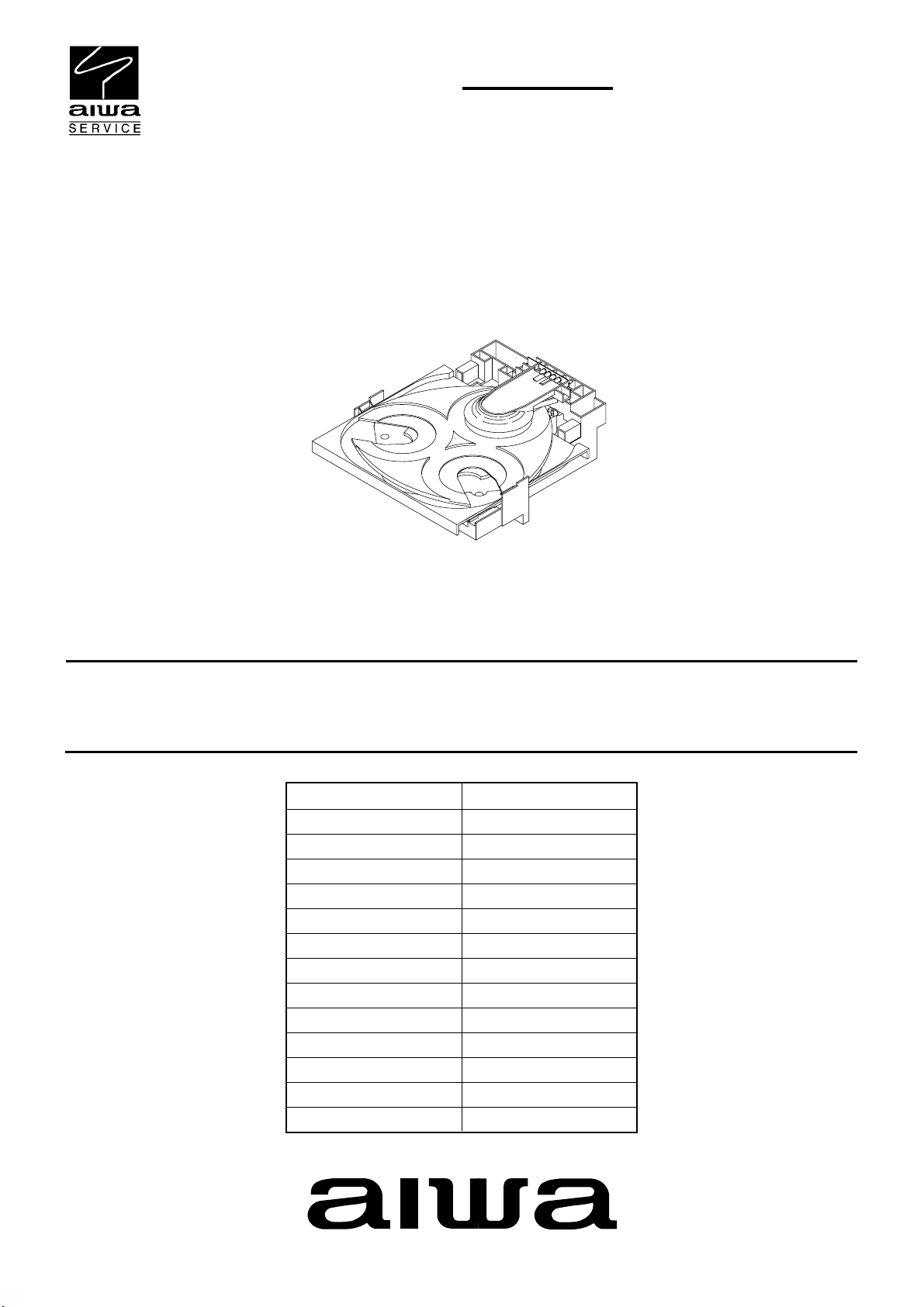
BASIC CD MECHANISM :ZA3:3ZG-2[E3]
CD-R/RW MECHANISM
TYPE
ZA3RDM
YZA3RDM
ZA3RNDM
YZA3RNDM
ZA3RN1DM
YKZA3RDF
YKZA3RNDF
ZA3RNM
YZA3RDCM
YZA3RNDCM
ZA4RDC
ZA4RNDC
ZA8RDC
ZA4:KSM-2131FAM
ZA8:KSM-880CAB
BASIC CD MECHANISM
3ZG-2 E3
3ZG-2 E3
3ZG-2 E3
3ZG-2 E3
3ZG-2 E3
3ZG-2 E3
3ZG-2 E3
3ZG-2 E3
3ZG-2 E3
3ZG-2 E3
KSM-2131 FAM
KSM-2131 FAM
KSM-880CAB
S/M Code No. 09-001-335-3NC
Page 2
PROTECTION OF EYES FROM LASER BEAM DURING SERVICING
CLASS 1
KLASSE 1
LUOKAN 1
KLASS 1
LASER PRODUCT
LASER PRODUKT
LASER LAITE
LASER APPARAT
This set employs laser. Therefore, be sure to follow carefully the
instructions below when servicing.
WARNING!
WHEN SERVICING, DO NOT APPROACH THE LASER EXIT
WITH THE EYE TOO CLOSELY. IN CASE IT IS NECESSARY TO
CONFIRM LASER BEAM EMISSION. BE SURE TO OBSERVE
FROM A DISTANCE OF MORE THAN 30cm FROM THE
SURFACE OF THE OBJECTIVE LENS ON THE OPTICAL
PICK-UP BLOCK.
Caution: Invisible laser radiation when
open and interlocks defeated avoid exposure to beam.
Advarsel:Usynling laserståling ved åbning,
når sikkerhedsafbrydere er ude af funktion.
Undgå udsættelse for stråling.
VAROITUS!
Laiteen Käyttäminen muulla kuin tässä käyttöohjeessa mainitulla tavalla saattaa altistaa käyt-täjän turvallisuusluokan 1 ylittävälle näkymättömälle lasersäteilylle.
CAUTION
Use of controls or adjustments or performance of procedures
other than those specified herein may result in hazardous
radiation exposure.
ATTENTION
L'utilisation de commandes, réglages ou procédures autres que
ceux spécifiés peut entraîner une dangereuse exposition aux
radiations.
ADVARSEL!
Usynlig laserståling ved åbning, når sikkerhedsafbrydereer ude
af funktion. Undgå udsættelse for stråling.
This Compact Disc player is classified as a CLASS 1 LASER
product.
The CLASS 1 LASER PRODUCT label is located on the rear
exterior.
VARNING!
Om apparaten används på annat sätt än vad som specificeras i
denna bruksanvising, kan användaren utsättas för osynling
laserstrålning, som överskrider gränsen för laserklass 1.
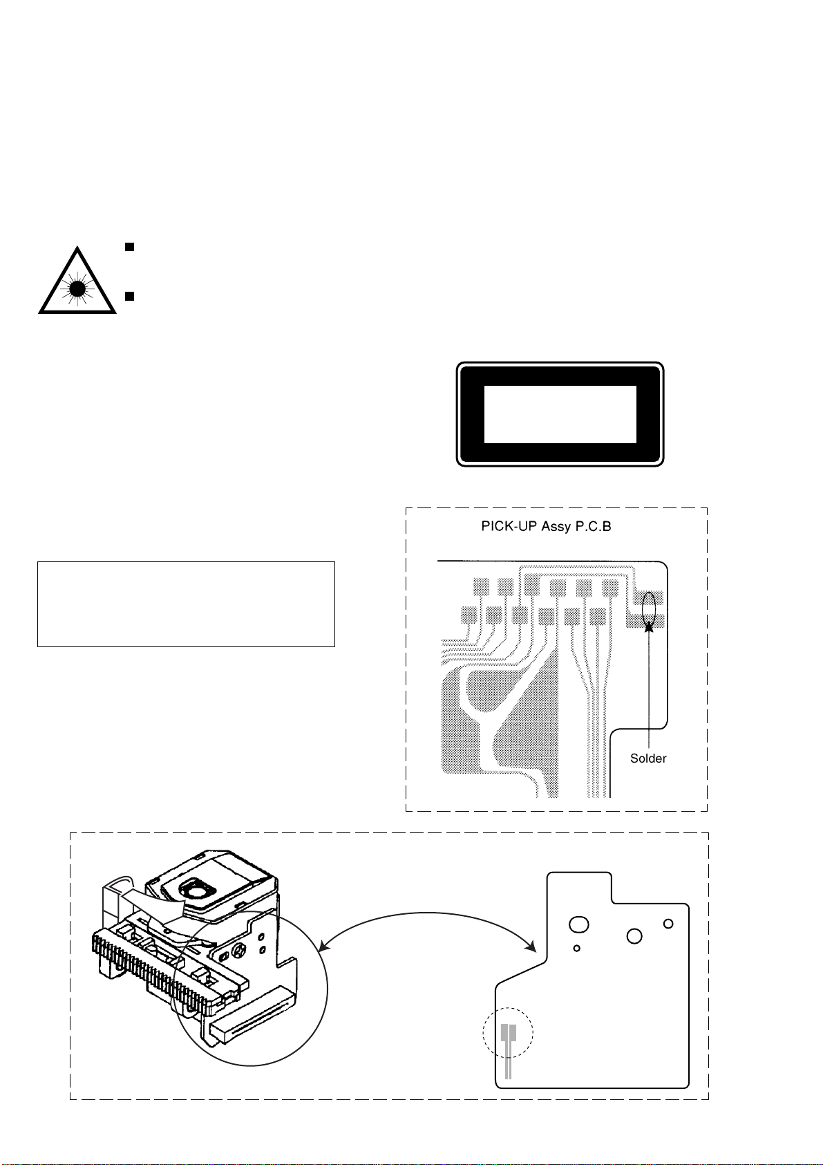
Precaution to replace Optical block
Body or clothes electrostatic potential could ruin
laser diode in the optical block. Be sure ground
body and workbench, and use care the clothes
do not touch the diode.
1) After the connection, remove solder shown in
the figure below.
ZA8 MODEL
ZA3/ZA4 MODEL (KSS-213F)
Solder
2
Page 3
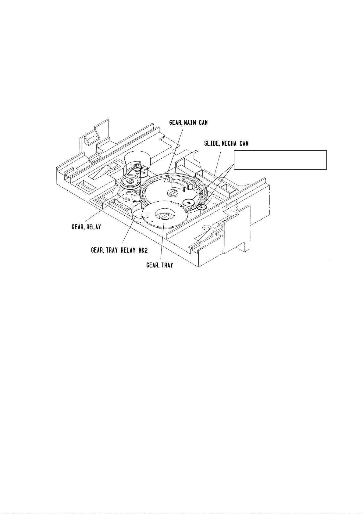
How to Adjust the Rotating Phase of the
Gear, Main Cam
1) Push down the hooking catch of the CHAS. MECH, and
remove the TRAY.
2) Align the arrow mark of the Gear, Main Cam with the black
round mark of the CHAS, MECHA as shown below.
3) Confirm that the Slide, Mech Cam is located in the right
position, then insert the TRAY gently.
Caution: If the rotating phase of the Gear, Main Cam is
incorrectly adjusted, the chucking operation and
tray movement will have malfunction.
Align the arrow 2 mark with the black
round • mark.
3
Page 4

ELECTRICAL MAIN PARTS LIST
REF. NO PART NO. KANRI DESCRIPTION
NO.
IC
87-A20-446-010 C-IC,LA9241ML
87-017-917-080 IC,BU4066BCF
87-A21-319-010 C-IC,LC78622NE
87-A20-445-010 IC,BA5936
TRANSISTOR
87-026-609-080 TR,KTA1266GR
87-026-239-080 TR,DTC114TK (0.2W)
87-026-295-080 TR,DTC144TK
87-A30-515-080
87-A30-087-080 C-FET,2SK2158
87-026-237-080 CHIP-TR,DTC124XK
<ZA3RDM,ZA4RDC,ZA3RDF,ZA8RDC,ZA3RDCM,YZA3RDM>
87-A30-076-080 C-TR,2SC3052F
87-A30-075-080 C-TR,2SA1235F<EXCEPT ZA3RNM>
DIODE
87-020-465-080 DIODE,1SS133 (110MA)
87-020-331-080 CHIP-DIODE,DAN202K
87-A40-337-080 ZENER,MTZJ 6.8B
87-A40-313-080 C-DIODE,MC 2840
87-A40-620-080 ZENER,MTZJ6.2A
3CD C.B
C11 87-012-393-080 C-CAP,S 0.22-16 R K
C12 87-012-157-080 C-CAP,S 330P-50 CH
<ZA4RDC,ZA4RNDC,ZA3RDF,ZA3RNDF,ZA8RDC,ZA3RDCM,ZA3RNDCM>
C12 87-012-157-020 C-CAP,S 330P-50 CH
<ZA3RN1DM,ZA3RDM,ZA3RNDM,ZA3RNM>
C13 87-016-369-080 C-CAP,S 0.033-25 B K
<ZA4RDC,ZA4RNDC,ZA3RDF,ZA3RNDF,ZA8RDC,ZA3RDCM,ZA3RNDCM>
C13 87-016-369-020 C-CAP,S 0.033-25 B K
<ZA3RN1DM,ZA3RDM,ZA3RNDM,ZA3RNM,YZA3RNDM,YZA3RDM>
C14 87-A10-201-080 C-CAP,S0.33-16 KB
C15 87-010-213-020 C-CAP,S 0.015-25 B
<ZA3RN1DM,ZA3RDM,ZA3RNDM,ZA3RNM,YZA3RNDM,YZA3RDM>
C15 87-010-213-080 C-CAP,S 0.015-50 B
<ZA4RDC,ZA4RNDC,ZA3RDF,ZA3RNDF,ZA8RDC,ZA3RDCM,ZA3RNDCM>
C16 87-010-992-080 C-CAP,S 0.047-25 B
C17 87-010-184-020 C-CAP,S 3300P-50 B
<ZA3RN1DM,ZA3RDM,ZA3RNDM,ZA3RNM,YZA3RNDM,YZA3RDM>
C17 87-010-184-080 CHIP CAPACITOR 3300P(K)
<ZA4RDC,ZA4RNDC,ZA3RDF,ZA3RNDF,ZA8RDC,ZA3RDCM,ZA3RNDCM>
C18 87-A11-177-080 C-CAP,S 0.15-16 K B
C19 87-010-992-080 C-CAP,S 0.047-25 B<ZA8RDC>
C19 87-010-198-080 CAP, CHIP 0.022<EXCEPT ZA8RDC>
C20 87-010-178-020 C-CAP,S 1000P-50 B
<ZA3RN1DM,ZA3RDM,ZA3RNDM,ZA3RNM,YZA3RNDM,YZA3RDM>
C20 87-010-178-080 CHIP CAP 1000P
<ZA4RDC,ZA4RNDC,ZA3RDF,ZA3RNDF,ZA8RDC,ZA3RDCM,ZA3RNDCM>
C21 87-012-393-080 C-CAP,S 0.22-16 R K
C22 87-016-083-080 C-CAP,S 0.15-16 RK
C23 87-010-197-020 C-CAP,S 0.01-25 B
<ZA3RN1DM,ZA3RDM,ZA3RNDM,ZA3RNM,YZA3RNDM,YZA3RDM>
C23 87-010-197-080 CAP, CHIP 0.01 DM
<ZA4RDC,ZA4RNDC,ZA3RDF,ZA3RNDF,ZA8RDC,ZA3RDCM,ZA3RNDCM>
C24 87-010-186-020 C-CAP,S 4700P-50 B
<ZA3RN1DM,ZA3RDM,ZA3RNDM,ZA3RNM,YZA3RNDM,YZA3RDM>
C24 87-010-186-080 CAP,CHIP 4700P
<ZA4RDC,ZA4RNDC,ZA3RDF,ZA3RNDF,ZA8RDC,ZA3RDCM,ZA3RNDCM>
C25 87-010-400-040 CAP,E 0.47-50
C26 87-010-322-080 C-CAP,S 100P-50 CH<ZA8RDC>
C26 87-010-176-020 C-CAP,S 680P-50 J SL
<ZA3RN1DM,ZA3RDM,ZA3RNDM,ZA3RNM,YZA3RNDM,YZA3RDM>
C26 87-010-176-080 C-CAP,S 680P-50 SL
<ZA4RDC,ZA4RNDC,ZA3RDF,ZA3RNDF,ZA3RDCM,ZA3RNDCM>
C27 87-010-382-040 CAP,E 22-25 SME
C28 87-010-545-040 CAP,E 0.22-50 SME
C29 87-010-184-020 C-CAP,S 3300P-50 B
<ZA3RN1DM,ZA3RDM,ZA3RNDM,ZA3RNM,YZA3RNDM,YZA3RDM>
REF. NO PART NO. KANRI DESCRIPTION
C29 87-010-184-080 CHIP CAPACITOR 3300P(K)
C31 87-010-186-020 C-CAP,S 4700P-50 B
C31 87-010-186-080 CAP,CHIP 4700P
C32 87-010-315-020 C-CAP,S 27P-50 CH
C32 87-010-315-080 C-CAP,S 27P-50 CH
C33 87-016-081-080 C-CAP,S 0.1-16 RK
C35 87-010-196-020 C-CAP,S 0.1-25 Z F GRM
C35 87-010-196-080 CHIP CAPACITOR,0.1-25
C37 87-010-405-080 CAP, ELECT 10-50V
C38 87-010-263-080 CAP, ELECT 100-10V
C39 87-010-992-080 C-CAP,S 0.047-25 B<EXCEPT ZA8RDC>
C39 87-010-197-080 CAP, CHIP 0.01 DM<ZA8RDC>
C40 87-010-401-080 CAP, ELECT 1-50V
C41 87-016-081-080 C-CAP,S 0.1-16 RK
C42 87-010-263-080 CAP, ELECT 100-10V
C43 87-010-197-020 C-CAP,S 0.01-25 B
C43 87-010-197-080 CAP, CHIP 0.01 DM
C44 87-010-263-080 CAP, ELECT 100-10V
C46 87-010-196-020 C-CAP,S 0.1-25 Z F GRM
C46 87-010-196-080 CHIP CAPACITOR,0.1-25
C47 87-010-260-080 CAP, ELECT 47-25V
C48 87-010-196-020 C-CAP,S 0.1-25 Z F GRM
C48 87-010-196-080 CHIP CAPACITOR,0.1-25
C49 87-010-404-080 CAP, ELECT 4.7-50V
C50 87-010-197-020 C-CAP,S 0.01-25 B
C50 87-010-197-080 CAP, CHIP 0.01 DM
C51 87-010-263-040 CAP,E 100-10
C52 87-012-156-020 C-CAP,S 220P-50 CH
C52 87-012-156-080 C-CAP,S 220P-50 CH
C53 87-010-381-080 CAP, ELECT 330-16V
C71 87-012-393-080 C-CAP,S 0.22-16 R K<ZA8RDC>
C80 87-010-196-020 C-CAP,S 0.1-25 Z F GRM
C80 87-010-196-080 CHIP CAPACITOR,0.1-25
C101 87-016-369-020 C-CAP,S 0.033-25 B K
C101 87-016-369-080 C-CAP,S 0.033-25 B K
C102 87-016-081-080 C-CAP,S 0.1-16 RK
C103 87-010-318-080 C-CAP,S 47P-50 CH
C103 87-010-318-020 C-CAP,S 47P-50 CH
C104 87-012-154-080 C-CAP,S 150P-50 CH
C104 87-012-154-020 C-CAP,S 150P-50 J CH GRM
C105 87-010-196-020 C-CAP,S 0.1-25 Z F GRM
C105 87-010-196-080 CHIP CAPACITOR,0.1-25
C109 87-010-197-020 C-CAP,S 0.01-25 B
C109 87-010-197-080 CAP, CHIP 0.01 DM
C111 87-010-312-080 C-CAP,S 15P-50 CH
NO.
<ZA4RDC,ZA4RNDC,ZA3RDF,ZA3RNDF,ZA8RDC,ZA3RDCM,ZA3RNDCM>
<ZA3RN1DM,ZA3RDM,ZA3RNDM,ZA3RNM,YZA3RNDM,YZA3RDM>
<ZA4RDC,ZA4RNDC,ZA3RDF,ZA3RNDF,ZA8RDC,ZA3RDCM,ZA3RNDCM>
<ZA3RN1DM,ZA3RDM,ZA3RNDM,ZA3RNM,YZA3RNDM,YZA3RDM>
<ZA4RDC,ZA4RNDC,ZA3RDF,ZA3RNDF,ZA8RDC,ZA3RDCM,ZA3RNDCM>
<ZA3RN1DM,ZA3RDM,ZA3RNDM,ZA3RNM,YZA3RNDM,YZA3RDM>
<ZA4RDC,ZA4RNDC,ZA3RDF,ZA3RNDF,ZA8RDC,ZA3RDCM,ZA3RNDCM>
<ZA3RN1DM,ZA3RDM,ZA3RNDM,ZA3RNM,YZA3RNDM,YZA3RDM>
<ZA4RDC,ZA4RNDC,ZA3RDF,ZA3RNDF,ZA8RDC,ZA3RDCM,ZA3RNDCM>
<ZA3RN1DM,ZA3RDM,ZA3RNDM,ZA3RNM,YZA3RNDM,YZA3RDM>
<ZA4RDC,ZA4RNDC,ZA3RDF,ZA3RNDF,ZA8RDC,ZA3RDCM,ZA3RNDCM>
<ZA3RN1DM,ZA3RDM,ZA3RNDM,ZA3RNM,YZA3RNDM,YZA3RDM>
<ZA4RDC,ZA4RNDC,ZA3RDF,ZA3RNDF,ZA8RDC,ZA3RDCM,ZA3RNDCM>
<ZA3RN1DM,ZA3RDM,ZA3RNDM,ZA3RNM,YZA3RNDM,YZA3RDM>
<ZA4RDC,ZA4RNDC,ZA3RDF,ZA3RNDF,ZA8RDC,ZA3RDCM,ZA3RNDCM>
<ZA3RN1DM,ZA3RDM,ZA3RNDM,ZA3RNM,YZA3RNDM,YZA3RDM>
<ZA4RDC,ZA4RNDC,ZA3RDF,ZA3RNDF,ZA8RDC,ZA3RDCM,ZA3RNDCM>
<EXCEPT ZA4RNDC>
<ZA3RN1DM,ZA3RDM,ZA3RNDM,ZA3RNM,YZA3RNDM,YZA3RDM>
<ZA4RDC,ZA4RNDC,ZA3RDF,ZA3RNDF,ZA8RDC,ZA3RDCM,ZA3RNDCM>
<ZA3RN1DM,ZA3RDM,ZA3RNDM,ZA3RNM,YZA3RNDM,YZA3RDM>
<ZA4RDC,ZA4RNDC,ZA3RDF,ZA3RNDF,ZA8RDC,ZA3RDCM,ZA3RNDCM>
<ZA4RDC,ZA4RNDC,ZA3RDF,ZA3RNDF,ZA8RDC,ZA3RDCM,ZA3RNDCM>
<ZA3RN1DM,ZA3RDM,ZA3RNDM,ZA3RNM,YZA3RNDM,YZA3RDM>
<ZA4RDC,ZA4RNDC,ZA3RDF,ZA3RNDF,ZA8RDC,ZA3RDCM,ZA3RNDCM>
<ZA3RN1DM,ZA3RDM,ZA3RNDM,ZA3RNM,YZA3RNDM,YZA3RDM>
<ZA3RN1DM,ZA3RDM,ZA3RNDM,ZA3RNM,YZA3RNDM,YZA3RDM>
<ZA4RDC,ZA4RNDC,ZA3RDF,ZA3RNDF,ZA8RDC,ZA3RDCM,ZA3RNDCM>
<ZA3RN1DM,ZA3RDM,ZA3RNDM,ZA3RNM,YZA3RNDM,YZA3RDM>
<ZA4RDC,ZA4RNDC,ZA3RDF,ZA3RNDF,ZA8RDC,ZA3RDCM,ZA3RNDCM>
<ZA4RDC,ZA4RNDC,ZA3RDF,ZA3RNDF,ZA8RDC,ZA3RDCM,ZA3RNDCM>
4
Page 5

REF. NO PART NO. KANRI DESCRIPTION
NO.
C111 87-010-312-020 C-CAP,S 15P-50 J CH
<ZA3RN1DM,ZA3RDM,ZA3RNDM,ZA3RNM,YZA3RNDM,YZA3RDM>
C112 87-010-154-020 C-CAP,S 10P-50 CH
<ZA3RN1DM,ZA3RDM,ZA3RNDM,ZA3RNM,YZA3RNDM,YZA3RDM>
C112 87-010-154-080 CAP CHIP 10P
<ZA4RDC,ZA4RNDC,ZA3RDF,ZA3RNDF,ZA8RDC,ZA3RDCM,ZA3RNDCM>
C113 87-010-178-020 C-CAP,S 1000P-50 B
<ZA3RN1DM,ZA3RDM,ZA3RNDM,ZA3RNM,YZA3RNDM,YZA3RDM>
C113 87-010-178-080 CHIP CAP 1000P
<ZA4RDC,ZA4RNDC,ZA3RDF,ZA3RNDF,ZA8RDC,ZA3RDCM,ZA3RNDCM>
C115 87-010-404-080 CAP, ELECT 4.7-50V
C116 87-010-196-020 C-CAP,S 0.1-25 Z F GRM
<ZA3RN1DM,ZA3RDM,ZA3RNDM,ZA3RNM,YZA3RNDM,YZA3RDM>
C116 87-010-196-080 CHIP CAPACITOR,0.1-25
<ZA4RDC,ZA4RNDC,ZA3RDF,ZA3RNDF,ZA8RDC,ZA3RDCM,ZA3RNDCM>
C117 87-010-263-040 CAP,E 100-10
C118 87-010-178-020 C-CAP,S 1000P-50 B
<ZA3RN1DM,ZA3RDM,ZA3RNDM,ZA3RNM,YZA3RNDM,YZA3RDM>
C118 87-010-178-080 CHIP CAP 1000P
<ZA4RDC,ZA4RNDC,ZA3RDF,ZA3RNDF,ZA8RDC,ZA3RDCM,ZA3RNDCM>
C119 87-010-194-080 CAP, CHIP 0.047<ZA3RN1DM>
C121 87-010-403-080 CAP, ELECT 3.3-50V
C122 87-010-403-080 CAP, ELECT 3.3-50V
C123 87-010-180-080 C-CER 1500P
C124 87-010-180-080 C-CER 1500P
C132 87-010-196-020 C-CAP,S 0.1-25 Z F GRM
<ZA3RN1DM,ZA3RDM,ZA3RNDM,ZA3RNM,YZA3RNDM,YZA3RDM>
C132 87-010-196-080 CHIP CAPACITOR,0.1-25
<ZA4RDC,ZA4RNDC,ZA3RDF,ZA3RNDF,ZA8RDC,ZA3RDCM,ZA3RNDCM>
C135 87-010-314-020 C-CAP,S 22P-50 CH
<ZA3RN1DM,ZA3RDM,ZA3RNDM,ZA3RNM,YZA3RNDM,YZA3RDM>
C135 87-010-314-080 C-CAP,S 22P-50V
<ZA4RDC,ZA4RNDC,ZA3RDF,ZA3RNDF,ZA8RDC,ZA3RDCM,ZA3RNDCM>
C191 87-010-263-040 CAP,E 100-10
C192 87-010-178-020 C-CAP,S 1000P-50 B
<ZA3RN1DM,ZA3RDM,ZA3RNDM,ZA3RNM,YZA3RNDM,YZA3RDM>
C192 87-010-178-080 CHIP CAP 1000P
<ZA4RDC,ZA4RNDC,ZA3RDF,ZA3RNDF,ZA8RDC,ZA3RDCM,ZA3RNDCM>
C193 87-010-196-020 C-CAP,S 0.1-25 Z F GRM
<ZA3RN1DM,ZA3RDM,ZA3RNDM,ZA3RNM,YZA3RNDM,YZA3RDM>
C193 87-010-196-080 CHIP CAPACITOR,0.1-25
<ZA4RDC,ZA4RNDC,ZA3RDF,ZA3RNDF,ZA8RDC,ZA3RDCM,ZA3RNDCM>
C201 87-010-196-020 C-CAP,S 0.1-25 Z F GRM
<ZA3RN1DM,ZA3RDM,ZA3RNDM,ZA3RNM,YZA3RNDM,YZA3RDM>
C201 87-010-196-080 CHIP CAPACITOR,0.1-25
<ZA4RDC,ZA4RNDC,ZA3RDF,ZA3RNDF,ZA8RDC,ZA3RDCM,ZA3RNDCM>
C204 87-010-196-020 C-CAP,S 0.1-25 Z F GRM
<ZA3RN1DM,ZA3RDM,ZA3RNDM,ZA3RNM,YZA3RNDM,YZA3RDM>
C204 87-010-196-080 CHIP CAPACITOR,0.1-25
<ZA4RDC,ZA4RNDC,ZA3RDF,ZA3RNDF,ZA8RDC,ZA3RDCM,ZA3RNDCM>
C205 87-010-196-020 C-CAP,S 0.1-25 Z F GRM
<ZA3RN1DM,ZA3RDM,ZA3RNDM,ZA3RNM,YZA3RNDM,YZA3RDM>
C205 87-010-196-080 CHIP CAPACITOR,0.1-25
<ZA4RDC,ZA4RNDC,ZA3RDF,ZA3RNDF,ZA8RDC,ZA3RDCM,ZA3RNDCM>
C206 87-010-196-020 C-CAP,S 0.1-25 Z F GRM
<ZA3RN1DM,ZA3RDM,ZA3RNDM,ZA3RNM,YZA3RNDM,YZA3RDM>
C206 87-010-196-080 CHIP CAPACITOR,0.1-25
<ZA4RDC,ZA4RNDC,ZA3RDF,ZA3RNDF,ZA8RDC,ZA3RDCM,ZA3RNDCM>
C207 87-010-196-020 C-CAP,S 0.1-25 Z F GRM
<ZA3RN1DM,ZA3RDM,ZA3RNDM,ZA3RNM,YZA3RNDM,YZA3RDM>
C207 87-010-196-080 CHIP CAPACITOR,0.1-25
<ZA4RDC,ZA4RNDC,ZA3RDF,ZA3RNDF,ZA8RDC,ZA3RDCM,ZA3RNDCM>
C208 87-010-196-020 C-CAP,S 0.1-25 Z F GRM
<ZA3RN1DM,ZA3RDM,ZA3RNDM,ZA3RNM,YZA3RNDM,YZA3RDM>
C208 87-010-196-080 CHIP CAPACITOR,0.1-25
<ZA4RDC,ZA4RNDC,ZA3RDF,ZA3RNDF,ZA8RDC,ZA3RDCM,ZA3RNDCM>
C211 87-010-405-040 CAP,E 10-50
C212 87-010-405-040 CAP,E 10-50
C213 87-010-196-020 C-CAP,S 0.1-25 Z F GRM
<ZA3RN1DM,ZA3RDM,ZA3RNDM,ZA3RNM,YZA3RNDM,YZA3RDM>
C213 87-010-196-080 CHIP CAPACITOR,0.1-25
<ZA4RDC,ZA4RNDC,ZA3RDF,ZA3RNDF,ZA8RDC,ZA3RDCM,ZA3RNDCM>
C251 87-010-322-020 C-CAP,S 100P-50 CH
<ZA3RDM,ZA3RNDM,ZA3RNM,YZA3RNDM,YZA3RDM>
C251 87-010-322-080 C-CAP,S 100P-50 CH
<ZA4RDC,ZA4RNDC,ZA3RDF,ZA3RNDF,ZA8RDC,ZA3RDCM,ZA3RNDCM>
REF. NO PART NO. KANRI DESCRIPTION
NO.
C252 87-010-322-080 C-CAP,S 100P-50 CH
<ZA4RDC,ZA4RNDC,ZA3RDF,ZA3RNDF,ZA8RDC,ZA3RDCM,ZA3RNDCM>
C252 87-010-322-020 C-CAP,S 100P-50 CH
<ZA3RN1DM,ZA3RDM,ZA3RNDM,ZA3RNM,YZA3RNDM,YZA3RDM>
C253 87-010-322-020 C-CAP,S 100P-50 CH
<ZA3RN1DM,ZA3RDM,ZA3RNDM,ZA3RNM,YZA3RNDM,YZA3RDM>
C253 87-010-322-080 C-CAP,S 100P-50 CH
<ZA4RDC,ZA4RNDC,ZA3RDF,ZA3RNDF,ZA8RDC,ZA3RDCM,ZA3RNDCM>
C254 87-010-322-020 C-CAP,S 100P-50 CH
<ZA3RN1DM,ZA3RDM,ZA3RNDM,ZA3RNM,YZA3RNDM,YZA3RDM>
C254 87-010-322-080 C-CAP,S 100P-50 J GH GRM
<ZA4RDC,ZA4RNDC,ZA3RDF,ZA3RNDF,ZA8RDC,ZA3RDCM,ZA3RNDCM>
C281 87-010-382-040 CAP,E 22-25 SME
C402 87-010-197-020 C-CAP,S 0.01-25 B
<ZA3RN1DM,ZA3RDM,ZA3RNDM,ZA3RNM,YZA3RNDM,YZA3RDM>
C402 87-010-197-080 CAP, CHIP 0.01 DM
<ZA4RDC,ZA4RNDC,ZA3RDF,ZA3RNDF,ZA8RDC,ZA3RDCM,ZA3RNDCM>
C403 87-010-196-020 C-CAP,S 0.1-25 Z F GRM
<ZA3RN1DM,ZA3RDM,ZA3RNDM,ZA3RNM,YZA3RNDM,YZA3RDM>
C403 87-010-196-080 CHIP CAPACITOR,0.1-25
<ZA4RDC,ZA4RNDC,ZA3RDF,ZA3RNDF,ZA8RDC,ZA3RDCM,ZA3RNDCM>
C404 87-010-260-040 CAP,E 47-25 SME
C405 87-010-382-080 CAP, ELECT 22-25V
C421 87-010-382-080 CAP, ELECT 22-25V
C422 87-010-196-020 C-CAP,S 0.1-25 Z F GRM
<ZA3RN1DM,ZA3RDM,ZA3RNDM,ZA3RNM,YZA3RNDM,YZA3RDM>
C422 87-010-196-080 CHIP CAPACITOR,0.1-25
<ZA4RDC,ZA4RNDC,ZA3RDF,ZA3RNDF,ZA8RDC,ZA3RDCM,ZA3RNDCM>
C901 87-010-260-080 CAP, ELECT 47-25V<EXCEPT ZA3RNM>
C902 87-010-196-020 C-CAP,S 0.1-25 Z F GRM
<ZA3RN1DM,ZA3RDM,ZA3RNDM,YZA3RNDM,YZA3RDM>
C902 87-010-196-080 CHIP CAPACITOR,0.1-25
<ZA4RDC,ZA4RNDC,ZA3RDF,ZA3RNDF,ZA8RDC,ZA3RDCM,ZA3RNDCM>
CN1 87-A60-429-010 CONN,16P H TOC-A
CN2 87-A60-081-010 CONN,06P H 9604S-06F
CN104 8A-ZA5-610-010 CONN ASSY,2P
CN201 87-099-030-010 CONN,13P 6216H
CN203 87-099-212-010 CONN,5P 6216 V
CN204 84-ZG1-648-010 CONN ASSY,6P
<ZA4RDC,ZA4RNDC,ZA8RDC>
CN204 87-099-199-010 CONN,6P 6216 H
<EXCEPT ZA4RDC,ZA4RNDC,ZA8RDC>
L11 87-005-849-080 COIL,10UH(CECS)
L101 87-005-614-080 COIL 100UH LAV35 J
L102 87-005-602-080 COIL,10UH LAV35 J
LED901 87-A40-558-010 LED,SLZ-8128A-01-A<EXCEPT ZA3RNM>
M201 87-045-383-010 MOT,M9I50T28-2
<ZA4RDC,ZA4RNDC,ZA8RDC>
M201 87-045-305-010 MOTOR, RF-500TB DC-5V (2MA)
<EXCEPT ZA4RDC,ZA4RNDC,ZA8RDC>
SFR101 87-A90-787-080 SFR,100K H HOKU
SW201 87-036-109-010 PUSH SWITCH
SW202 87-036-109-010 PUSH SWITCH
X101 87-A70-046-010 VIB,XTAL 16.934MHZ
LED C.B<ZA3RDM,ZA4RDC,ZA3RDF,ZA8RDC,ZA3RDCM,YZA3RDM>
LED302 87-A40-263-080 LED,SLH-56PCT31 GRN
<ZA3RDM,ZA4RDC,ZA3RDF,ZA8RDC,ZA3RDCM,YZA3RDM>
LED303 87-A40-268-080 LED,SLH-56DCT31 ORN
<ZA3RDM,ZA4RDC,ZA3RDF,ZA8RDC,ZA3RDCM,YZA3RDM>
T-T C.B
C401 87-A11-148-080 CAP,TC U 0.1-50 Z F
CN401 87-A60-082-010 CONN,05P H 9604S-05F
<ZA3RN1DM,ZA3RDM,ZA4RDC,ZA4RNDC,ZA3RDF,ZA3RNDF,YZA3RDM>
CN401 86-NFZ-675-010 CONN,5P H 6216-11H
<ZA3RNDM,ZA3RNM,ZA8RDC,ZA3RDCM,ZA3RNDCM,YZA3RNDM>
M401 87-045-364-010 MOTOR(BCH3B14)
PS401 87-026-573-010 SNSR,PHOTO GP1S53V
<EXCEPT ZA3RN1DM,ZA3RDM,ZA4RDC,ZA3RDF,ZA3RNDF,YZA3RDM>
PS401 87-A90-156-010 SNSR,SG-240
<ZA3RN1DM,ZA3RDM,ZA4RDC,ZA3RDF,ZA3RNDF,YZA3RDM>
5
Page 6
REF. NO PART NO. KANRI DESCRIPTION
NO.
DRIVE C.B<EXCEPT ZA4RDC,ZA4RNDC,ZA8RDC>
M1 87-045-358-010 MOT,RF-310TA 43
<EXCEPT ZA4RDC,ZA4RNDC,ZA8RDC>
M2 87-045-356-010 MOT,RF-310TA 30
<EXCEPT ZA4RDC,ZA4RNDC,ZA8RDC>
PIN3 87-A60-086-010 CONN,6P H6216-11
<EXCEPT ZA4RDC,ZA4RNDC,ZA8RDC>
SW1 87-A90-042-010 SW,LEAF MSW-17310MVP0
<EXCEPT ZA4RDC,ZA4RNDC,ZA8RDC>
• Regarding connectors, they are not stocked as they are not the initial order items.
The connectors are available after they are supplied from connector manufacturers upon the order is received.
CHIP RESISTOR PART CODE
REF. NO PART NO. KANRI DESCRIPTION
NO.
MOTOR C.B<ZA4RDC,ZA4RNDC>
M2 9X-262-513-210 SLED MOTOR<ZA4RDC,ZA4RNDC>
PIN3 91-564-722-110 CONNECTOR 6P<ZA4RDC,ZA4RNDC>
SW1 91-572-085-110 LEAF SW<ZA4RDC,ZA4RNDC>
MOTOR C.B<ZA8RDC>
PIN3 91-564-722-110 CONN,PIN 6P<ZA8RDC>
SW1 91-572-085-110 LEAF SWITCH<ZA8RDC>
Chip Resistor Part Coding
88
A
Resistor Code
Chip resistor
Wattage Type Tolerance
1/16W 1005 5% CJ
1/16W
1/10W
1/8W
1608
2125
3216
5%
5%
5%
TRANSISTOR ILLUSTRATION
C
Symbol
CJ
CJ
CJ
Figure
Value of resistor
Form
L
Dimensions (mm)
t
W
0.55
Resistor Code
108
118
128
LW t
1.0 0.5 0.35 104
1.6 0.8 0.45
2 1.25 0.45
3.2
1.6
: A
: A
ECB
KTA1266
B
E
2SA1235
2SC3052
2SK2158
DTC114TK
DTC124XK
DTC144TK
6
Page 7
BLOCK DIAGRAM
EXCEPT ZA3RNM
87
Page 8

WIRING-1 (3CD/LED)
1
234567
8
ZA3 MODEL
9
TO DRIVE C.B
10
11 12 13
14
A
ZA4/ZA8 MODEL
B
C
D
E
F
G
H
I
J
K
109
Page 9

SCHEMATIC DIAGRAM
MOTOR C.B
(ZA4/ZA8)
DRIVE C.B
(ZA3)
1211
Page 10

WIRING-2 (T-T/MOTOR)
VREF
VREF
1
A
B
C
D
234567
ZA3 MODEL
ZA4 MODEL
WAVE FORM
1 IC11 Pin = (RFSH) VOLT/DIV: 0.5V
TIME/DIV: 1µS
MAX
1.7±0.1 Vp-p
0 V
EYE PATTERN
must be CLEAR and MAX
2 IC11 Pin ^ (FD) VOLT/DIV: 100mV
TIME/DIV: 1mS
VREF
4 IC11 Pin ≥ (SPD) VOLT/DIV: 100mV
TIME/DIV: 1mS
VREF
5 IC11 Pin ª (SLD) VOLT/DIV: 200mV
TIME/DIV: 2S
E
F
G
H
I
3 IC11 Pin % (TO) VOLT/DIV: 100mV
TIME/DIV: 1mS
ZA8 MODEL
IC BLOCK DIAGRAM
IC, BA5936S
J
K
1413
Page 11

TEST MODE
1. How to Activate CD Test Mode
Insert the AC plug while pressing the function CD button.
All FL display tubes will light up, and the test mode will be
activated.
3. CD Test Mode Functions
When test mode is activated, the following mode functions from No.1 to No.5 can be used by pressing the operation keys.
2. How to Cancel CD Test Mode
Either one of the following operations will cancel the CD test
mode.
• Press the function button. • Press the power switch button.
(except CD function button) • Disconnect the AC plug
Mode/No.
Start mode
No.1
Search mode
No.2
Play mode
No.3
Traverse mode
No.4
Sled mode
No.5
Operation
Activation
9 key
1 2 key
key
;
fi key
fl
FL display
All lamps light
All lamps light
Operation
• Test mode is activated.
• CD block power is ON.
• Laser diode turns always ON.
• Continual focus search
(The pickup lens repeats the fullswing up-down motion.)
* Avoid continual searches that last for
more than 10 minutes.
* NOTE 1
• Normal playback
• Focus search is continued if TOC
cannot be read. * NOTE 1
• During normal disc playback
Press once; tracking servo OFF
Press twice; tracking servo ON
* NOTE 2
• Pickup moves to the outermost track
• Pickup moves to the innermost track
* NOTE 3
(During playback, machine operates
normally.)
Contents
• FL display check (All displays light.)
• APC circuit check
• Laser current measurement
(Laser current control. Across a
resistor connected between emitter
and GND.)
FOCUS SERVO
• Check focus search waveform
• Check focus error waveform
(FOK/FZC are not monitored in the
search mode)
FOCUS SERVO/TRACKING SERVO
CLV SERVO/SLED SERVO
Check DRF
TRACKING SERVO ON/OFF
Tracking balance (traverse) check
SLED SERVO
Check SLED mechanism operation
* NOTE 1: There are cases when the tracking servo cannot be locked owing to the protection circuit being operated when heat builds up
in the driver IC if the focus search is operated continually for more than 10 minutes. In these cases the power supply should be
switched off for 10 minutes until heat has been reduced and then re-started.
* NOTE 2: Do not press the fi or fl keys when the machine is in the
after the
status has been canceled. If the fi or fl keys are pressed in the ; status, press the 9 key and return to the start mode
;
status is active. If they are pressed, playback will not be possible
;
(No.1).
* NOTE 3: When pressing the fi or fl keys, take care to avoid damage to the gears. Because the sled motor is activated when the fi or fl
keys are pressed, even when the pick-up is at the outermost or innermost track.
4. Operation Outline
The operation of each mode is carried out in the direction of the arrows from the start mode as indicated in the following illustration.
No. 2 No. 3
1 2
No. 1
Start mode
(All FLs light up.)
2
Search mode
9
9
fi
fl
No. 5 No. 4
Sled mode
;
Play mode
9
1 2
;
;
9
Traverse mode
If the DISC DIRECT PLAY button is pressed, the machine performs the same operation as the PLAY button is pressed as shown. If
the tray is opened by pressing OPEN/CLOSE button during Play mode or Traverse mode, the machine returns to the Start mode.
15
Page 12

IC DESCRIPTION
IC, LC78622NE
Pin No. Pin Name I/O Description
1
2
3
DEFI
TAI
PDO
I
Defect sense signal (DEF) input pin. (Connect to 0V when not used).
I
O
Test signal input pin with built-in pull-down resistor. Be sure to connect to 0V.
Phase comparator output pin to control external VCO.
4
5
6
7
8
9
10
11
12, 13
14
15
16
17
18
19, 20
21
VVSS
ISET
VVDD
FR
VSS
EFMO
EFMIN
TEST2
CLV+, CLV–
___
V/P
HFL
TES
TOFF
TGL
JP+, JP–
PCK
—
—
—
For PLL.
I
I
Digital system GND. Be sure to connect to 0V.
O
For slice level control.
I
I
Test signal input pin with built-in pull-down resistor. Be sure to connect to 0V.
O
Disc motor control output. Three level output is possible using command.
Rough servo or phase control automatic selection monitoring output pin. Rough servo
O
at H. Phase servo at L.
I
Track detect signal input pin. Schmidt input.
I
Tracking error signal input pin. Schmidt input.
O
Tracking OFF output pin.
O
Tracking gain selection output pin. Gain boost at L.
O
Track jump control signal output pin. Three level output is possible using command.
O
EFM data playback clock monitoring pin 4.3218 MHz when phase is locked in.
GND pin for built-in VCO. Be sure to connect to 0V.
Pin to which external resistor adjusting the PD0 output current.
Power supply pin for built-in VCO.
Pin for VCO frequency range adjustment.
EFM signal output pin.
EFM signal input pin.
22
23
24
25
26
27
28
29
30
31
32, 33
34
35
36
37
38
39
40
41
FSEQ
VDD
SLD+
SLD-
PUSW
RW
LENSDW
EMPH
C2F
DOUT
TEST3, TEST4
N.C.
MUTEL
LVDD
LCHO
LVSS
RVSS
RCHO
RVDD
O
—
I/O
I/O
I/O
I/O
I/O
O
O
O
—
O
—
O
—
—
O
—
Sync signal detection output pin. H when the sync signal which is detected from EFM
signal and thesync signal which is internally generated agree.
Digital system power supply pin.
The pin is controlled by the serial data
command from microprocessor. When
General purpose input/output pin 1 to 5.
De-emphasis monitor output pin. De-emphasis disc is being played back at H.
C2 flag output pin.
DIGITAL OUT output pin. (EIAJ format).
I
Test signal input pin with built-in pull-down resistor. Be sure to connect to 0V.
Not used. Set the pin to open.
L-channel mute output pin.
L-channel 1-bit DAC.
R-channel 1-bit DAC.
L-channel power supply pin.
L-channel output pin.
L-channel GND. Be sure to connect to 0V.
R-channel GND. Be sure to connect to 0V.
R-channel output pin.
R-channel power supply pin.
the pin is not used, set the pin to the input
terminal and connect to 0V, or alternately
set the pin to output terminal and leave
the pin open.
42
MUTER
O
16
R-channel mute output pin.
Page 13

Pin No. Pin Name I/O Description
43
44
45
46
47
XVDD
XOUT
XIN
XVSS
SBSY
—
Crystal oscillator power supply pin.
O
Pin to which external 16.9344 MHz crystal oscillator is connected.
I
—
Crystal oscillator GND pin. Be sure to connect to 0V.
O
Subcode block sync signal output pin.
48
49
50
51
52
53
54
55
56
57
58
59
60
61
62
63
64
EFLG
PW
SFSY
SBCK
FSX
WRQ
RWC
SQOUT
COIN
___________
CQCK
________
RES
TST11
16M
4.2M
TEST5
______
CS
TEST1
O
C1, C2, single and dual correction monitoring pin.
O
Subcode P, Q, R, S, T, U and W output pin.
O
Subcode frame sync signal output pin. Falls down when subcode enters standby.
Subcode read clock input pin. Schmidt input. (Be sure to connected to 0V when not
I
in use.)
Pin outputting the 7.35 kHz sync signal which is generated by dividing frequency of
O
crystal oscillator.
O
Subcode Q output standby output pin.
I
Read/write control input pin. Schmidt input.
O
Subcode Q output pin.
I
Command input pin from microprocessor.
I
Command input read clock or subcode read input clock from SQOUT pin
I
LC78622 reset input pin. Set this pin to L once when the main power is turned on.
O
Test signal output pin. Use this pin as open (normally L output).
O
16.9344 MHz output pin.
O
4.2336 MHz output pin.
I
Test signal input pin with built-in pull-down resistor. Be sure to connect to 0V.
Chip select signal input pin with built-in pull-down resistor. Be sure to connect to 0V
I
while it is not controlling.
I
Test signal input pin without built-in pull-down resistor. Be sure to connect to 0V.
Note: The same potential must be applied to the respective power supply terminals. (VDD, VVDD, LVDD, RVDD, XVDD)
17
Page 14

IC, LA9241ML
Pin No. Pin Name I/O Description
1
2
FIN2
FIN1
Pin to which external pickup photo diode is connected. RF signal is created by adding
I
with the FIN1 pin signal. FE signal is created by subtracting from the FIN1 pin signal.
I
Pin to which external pickup photo diode is connected.
10
11
12
13
14
15
16
17
3
4
5
6
7
8
9
E
F
TB
TE–
TE
TESI
SCI
TH
TA
TD–
TD
JP
TO
FD
FD–
Pin to which external pickup photo diode is connected. TE signal is created by
I
subtracting from the F pin signal.
I
Pin to which external pickup photo diode is connected.
I
DC component of the TE signal is input.
I
Pin to which external resistor setting the TE signal gain is connected between the TE pin.
O
TE signal output pin.
TES “Track Error Sense” comparator input pin. TE signal is passed through a band-
I
pass filter then input.
I
Shock detection signal input pin.
I
Tracking gain time constant setting pin.
O
TA amplifier output pin.
Pin to which external tracking phase compensation constants are connected between
I
the TD and VR pins.
I
Tracking phase compensation setting pin.
I
Tracking jump signal (kick pulse) amplitude setting pin.
O
Tracking control signal output pin.
O
Focusing control signal output pin.
Pin to which external focusing phase compensation constants are connected between
I
the FD and FA pins.
18
19
20
21
22
23
24
25
26
27
28
29
30, 31
32, 33
34
FA
FA–
FE
FE–
PGND
SP
SP1
SPG
SP–
SPD
SLED
SLD
SL–, SL+
JP–, JP+
TGL
—
—
Pin to which external focusing phase compensation constants are connected between
I
the FD– and FA– pins.
Pin to which external focusing phase compensation constants are connected between
I
the FA and FE pins.
O
FE signal output pin.
I
Pin to which external FE signal gain setting resistor is connected between the FE pin.
Analog signal GND.
No connection.
O
Single ended output of the CV+ and CV– pin input signal.
I
Pin to which external spindle gain setting resistor in 12 cm mode is connected.
Pin to which external spindle phase compensation constants are connected together
I
with SPD pin.
O
Spindle control signal output pin.
I
Pin to which external sled phase compensation constants are connected.
O
Sled control signal output pin.
I
Sled advance signal input pin from microprocessor.
I
Tracking jump signal input pin from DSP.
I
Tracking gain control signal input from DSP. Low gain when TGL = H.
35
TOFF
I
Tracking off control signal input pin from DSP. Off when TOFF = H.
18
Page 15

Pin No. Pin Name I/O Description
36
TES
O
Pin from which TES signal is output to DSP.
37
38
39, 40
41
42
43
44
45
46
47
48
49
50
51
52
53
54
55
HFL
SLOF
CV–, CV+
RFSH
RFS–
SLC
SLI
DGND
FSC
TBC
NC
DEF
CLK
CL
DAT
CE
DRF
NC
“High Frequency Level” is used to judge whether the main beam position is on top of
O
bit or on top of mirror.
I
Sled servo off control input pin.
I
CLV error signal input pin from DSP.
O
RF output pin.
RF gain setting and EFM signal 3T compensation constant setting pin together with
I
RFSM pin.
“Slice Level Control” is the output pin which controls the RF signal data slice level by
O
DSP.
I
Input pin which control the data slice level by the DSP.
—
Digital system GND.
O
Output pin to which external focus search smoothing capacitor is connected.
I
“Tracking Balance Control” EF balance variable range setting pin.
—
No connection.
O
Disc defect detector output pin.
I
Reference clock input pin. 4.23 MHz of the DSP is input.
I
Microprocessor command clock input pin.
I
Microprocessor command data input pin.
I
Microprocessor command chip enable input pin.
O
“Detect RF” RF level detector output.
I
No connection.
56
57
58
59
60
61
62
63
64
VCC2
REF1
VR
LF2
PH1
BH1
LDO
LDS
VCC1
—
Servo system and digital system Vcc pin.
—
Pin to which external bypass capacitor for reference voltage is connected.
O
Reference voltage output pin.
I
Disc defect detector time constant setting pin.
I
Pin to which external capacitor for RF signal peak holding is connected.
I
Pin to which external capacitor for RF signal bottom holding is connected.
O
APC circuit output pin.
I
APC circuit input pin.
—
RF system Vcc pin.
19
Page 16

MECHANICAL EXPLODED VIEW 1/1
13
11
12
14
28
27
26
25
24
23
22
B
29
C
19
30
a
A
31
20
P.C .B
21
P.C.B
10
a
32
9
4
8
18
7
6
3
4
1
2
5
CUSHION,CD A
15
AZA-5 P.C.B
17
16
EXCEPT ZA4, ZA8 : 3ZG-2
ZA4 : KSM-2131FAM
ZA8 : KSM-880CAB
20
CUSHION,CD A
33 (EXCEPT ZA4, ZA8)
15
CUSHION,CD A
Page 17

MECHANICAL PARTS LIST 1/1
REF. NO PART NO. KANRI DESCRIPTION
NO.
1 84-ZG1-225-010 BELT,SQ1.0-63.3
2 84-ZG1-672-010 F-CABLE,5P 1.25 210MM WHITE N
3 87-045-364-010 MOTOR(BCH3B14)
4 84-ZG1-267-010 PULLEY,LOAD MO 8
<EXCEPT ZA3RDF,ZA3RNDF>
4 81-ZG1-212-010 PULLY,LOAD MO<ZA3RDF,ZA3RNDF>
5 84-ZG1-238-010 GEAR,WORM N
6 84-ZG1-248-010 SPR-C,WORM
7 84-ZG1-273-010 PULLEY,WORM 4
<ZA4RDC,ZA4RNDC,ZA8RDC>
7 84-ZG1-239-210 PULLY,WORM N
<EXCEPT ZA4RDC,ZA4RNDC,ZA8RDC>
8 8A-ZG1-001-010 TRAY,NO3 BLU
9 84-ZG1-291-110 HLDR,MAGNET 4 NAT
<ZA3RNDM,ZA4RNDC,ZA3RNDF,ZA3RNM,ZA3RNDCM>
9 84-ZG1-272-110 HLDR,MAGNET N 4
<ZA3RN1DM,ZA3RDM,ZA4RDC,ZA3RDF,ZA8RDC,ZA3RDCM>
10 84-ZG1-259-010 SPR-P,WORM
11 84-ZG1-221-010 GEAR,MAIN TT<ZA3RDF,ZA3RNDF>
11 84-ZG1-269-010 GEAR,MAIN TT 4
<EXCEPT ZA3RDF,ZA3RNDF>
12 84-ZG1-224-010 LEVER,TT
<ZA3RN1DM,ZA3RDM,ZA4RDC,ZA3RDF,ZA8RDC,ZA3RDCM>
12 84-ZG1-288-010 LEVER,TT NAT
<ZA3RNDM,ZA4RNDC,ZA3RNDF,ZA3RNM,ZA3RNDCM>
13 8A-ZG1-002-010 TURN TABLE,NO1 BLU
14 81-ZG1-239-010 S-SCREW,TT
15 81-ZG1-271-010 S-SCREW MECH REAR<EXCEPT ZA8RDC>
15 8A-ZG1-201-010 S-SCREW,MECH 880<ZA8RDC>
16 85-NFT-611-110 FF-CABLE 16P-1.0
17 84-ZG1-287-010 HLDR,MECHA NAT
<ZA3RNDM,ZA4RNDC,ZA3RNDF,ZA3RNM,ZA3RNDCM>
17 84-ZG1-212-210 HLDR,MECHA NO2
<ZA3RN1DM,ZA3RDM,ZA4RDC,ZA3RDF,ZA3RDCM>
17 84-ZG1-299-310 HLDR,MECHA NO3<ZA8RDC>
18 87-045-383-010 MOT,M9I50T28-2
<ZA4RDC,ZA4RNDC,ZA8RDC>
18 87-045-305-010 MOTOR, RF-500TB DC-5V (2MA)
<EXCEPT ZA4RDC,ZA4RNDC,ZA8RDC>
19 84-ZG1-211-010 SPR-E CAM S
20 84-ZG1-285-010 PLATE,MAGNET BLK<ZA3RN1DM>
20 81-ZG1-255-110 PLATE,MAGNET MK2<EXCEPT ZA3RN1DM>
REF. NO PART NO. KANRI DESCRIPTION
21 83-ZG3-604-010 RING,MAG 2
22 83-ZG3-213-010 LVR,SW
23 84-ZG1-208-210 LEVER,CAM
23 84-ZG1-266-010 LEVER,CAM 8
24 84-ZG1-205-210 GEAR,TRAY (*)
25 81-ZG1-250-110 GEAR,TRAY RELAY MK2*
25 81-ZG1-291-110 GEAR,TRAY RELAY NO3
26 84-ZG1-206-110 GEAR,RELAY
26 84-ZG1-274-010 GEAR,RELAY 8
27 84-ZG1-207-010 PULLEY,RELAY
27 84-ZG1-271-010 PULLEY,RELAY 8
28 84-ZG1-209-010 BELT,SQ1.8-117.7
29 84-ZG1-203-410 GEAR,MAIN CAM
29 84-ZG1-215-410 GEAR,MAIN CAM BLU
30 84-ZG1-011-010 REFLECTOR,CD
31 84-ZG1-216-310 SLIDE,MECHA CAM YEL
31 84-ZG1-204-310 SLIDER,MECHA CAM
32 84-ZG1-201-410 CHAS,MECHA
32 84-ZG1-232-210 CHAS,MECHA N<ZA4RDC,ZA8RDC>
32 84-ZG1-292-010 CHAS,MECHA N NAT<ZA4RNDC>
32 84-ZG1-286-010 CHAS,MECHA NAT
33 84-ZG1-630-010 CABLE FFC 6P-1.25
A 87-067-703-010 TAPPING SCREW, BVT2+3-10
B 87-067-981-010 BVT2+3-6 BLK
C 87-251-070-410 U+2.6-3<ZA4RDC,ZA4RNDC,ZA8RDC>
NO.
<ZA4RDC,ZA4RNDC,ZA3RDF,ZA3RNDF,ZA8RDC>
<EXCEPT ZA4RDC,ZA4RNDC,ZA3RDF,ZA3RNDF,ZA8RDC>
<ZA4RDC,ZA4RNDC,ZA8RDC>
<EXCEPT ZA4RDC,ZA4RNDC,ZA8RDC>
<ZA4RDC,ZA4RNDC,ZA3RDF,ZA3RNDF,ZA8RDC>
<EXCEPT ZA4RDC,ZA4RNDC,ZA3RDF,ZA3RNDF,ZA8RDC>
<EXCEPT ZA4RDC,ZA4RNDC,ZA8RDC>
<ZA4RDC,ZA4RNDC,ZA8RDC>
<ZA3RNDM,ZA4RNDC,ZA3RNDF,ZA3RNM,ZA3RNDCM>
<ZA3RN1DM,ZA3RDM,ZA4RDC,ZA3RDF,ZA8RDC,ZA3RDCM>
<ZA3RDM,ZA4RDC,ZA3RDF,ZA8RDC,ZA3RDCM>
<ZA3RN1DM,ZA3RDM,ZA4RDC,ZA3RDF,ZA8RDC,ZA3RDCM>
<ZA3RNDM,ZA4RNDC,ZA3RNDF,ZA3RNM,ZA3RNDCM>
<ZA3RN1DM,ZA3RDM,ZA3RDF,ZA3RDCM>
<ZA3RNDM,ZA3RNDF,ZA3RNM,ZA3RNDCM>
<EXCEPT ZA4RDC,ZA4RNDC,ZA8RDC>
<ZA3RDM,ZA4RDC,ZA3RDF,ZA8RDC,ZA3RDCM>
COLOR NAME TABLE
Basic color symbol Color Basic color symbol Color Basic color symbol Color
B Black C Cream D Orange
G Green H Gray L Blue
LT Transparent Blue N Gold P Pink
R Red S Silver ST Titan Silver
T Brown V Violet W White
WT Transparent White Y Yellow YT Transparent Yellow
LM Metallic Blue LL Light Blue GT Transparent Green
LD Dark Blue DT Transparent Orange
21
Page 18

CD MECHANISM EXPLODED VIEW 1/1 (3ZG-2E3)
9
7
8
2
10
6
A
A
A
A
1
5
3
SW1
4
M1
M2
P.C.B
CD MECHANISM PARTS LIST 1/1 (3ZG-2E3)
REF. NO PART NO. KANRI DESCRIPTION
NO.
1 83-ZG2-243-310 CHAS ASSY,SHT
2 83-ZG2-235-010 GEAR,A3
3 83-ZG2-205-210 GEAR,B
4 83-ZG2-236-010 GEAR,MOTOR 3
5 83-ZG2-253-110 SHAFT,SLIDE 5
6 87-A90-836-010 PICKUP,KSS-213F
7 83-ZG2-227-310 TURN TABLE,C1
8 83-ZG2-245-510 LEVER,SHUTTER(*)
9 83-ZG2-250-110 SPR-E,SHT 2
10 83-ZG2-241-110 PLATE,C2
A 87-261-032-210 V+2-3
22
Page 19

CD MECHANISM EXPLODED VIEW 1/1 (KSM-2131 FAM)
6
7
3
2
COVER
5
SPINDLE MOTOR
4
CD MECHANISM PARTS LIST 1/1 (KSM-2131 FAM)
A
1
MOTOR C.B
REF. NO PART NO. KANRI DESCRIPTION
1 9X-264-629-220 MOTOR CHASSIS ASSY(MB)(FR)
2 92-626-907-010 GEAR(A)(S)
3 87-A90-836-010 OPTICAL PICK UP KSS-213F
4 92-626-908-020 SHAFT SLED
5 92-627-003-010 GEAR(B)
6 92-646-697-020 LENS SHUTTER(F)
7 92-646-702-010 SPRIG EXTENSION
A 97-621-255-150 SCREW+P2-3
NO.
23
Page 20

CD MECHANISM EXPLODED VIEW 1/1 (KSM-880CAB)
8
6
4
5
2
7
A
9
10
11
3
P.C. B
1
CD MECHANISM PARTS LIST 1/1 (KSM-880CAB)
REF. NO PART NO. KANRI DESCRIPTION
1 91-564-722-110 CONN,PIN 6P
2 91-572-085-110 LEAF SWITCH
3 9X-264-655-010 SL MOTORR ASSY
4 M8-ZZK-C90-070 KSM-880CAB
5 92-647-416-020 SPRING EXTENSION
6 92-647-595-020 SHUTTER B
7 92-647-732-010 NS SLIDE RACK
8 92-647-742-010 SPRING COMPRESSION
9 93-321-813-110 POLI WASHER
10 92-647-407-010 GEAR A
11 92-647-408-020 GEAR B
A 93-713-786-510 SCREW,+P2-3
NO.
24
Page 21

REFERENCE NAME LIST
ELECTRICAL SECTION
DESCRIPTION REFERENCE NAME
ANT ANTENNAS
C- CHIP
C-CAP CAP, CHIP
C-CAP TN CAP, CHIP TANTALUM
C-COIL COIL, CHIP
C-DI DIODE, CHIP
C-DIODE DIODE, CHIP
C-FET FET, CHIP
C-FOTR FILTER, CHIP
C-JACK JACK, CHIP
C-LED LED, CHIP
C-RES RES, CHIP
C-SFR SFR, CHIP
C-SLIDE SW SLIDE SWITCH, CHIP
C-SW SWITCH, CHIP
C-TR TRANSISTOR, CHIP
C-VR VOLUME, CHIP
C-ZENER ZENER, CHIP
CAP, CER CAP, CERA-SOL
CAP, E CAP, ELECT
CAP, M/F CAP, FILM
CAP, TC CAP, CERA-SOL
CAP, TC-U CAP, CERA-SOL SS
CAP, TN CAP, TANTALUM
CERA FIL FILTER, CERAMIC
CF FILTER, CERAMIC
DL DELAY LINE
E/CAP CAP, ELECT
FILT FILTER
FLTR FILTER
FUSE RES RES, FUSE
MOT MOTOR
P-DIODE PHOTO DIODE
P-SNSR PHOTO SENSER
P-TR PHOTO TRANSISTOR
POLY VARI VARIABLE CAPACITOR
PPCAP CAP, PP
PT POWER TRANSFORMER
PTR, RES PTR, MELF
RC REMOTE CONTROLLER
RES NF RES, NON-FLAMMABLE
RESO RESONATOR
SHLD SHIELD
SOL SOLENOID
SPKR SPEAKER
SW, LVR SWITCH, LEVER
SW, RTRY SWITCH, ROTARY
SW, SL SWITCH, SLIDE
TC CAP CAP, CERA-SOL
THMS THERMISTOR
TR TRANSISTOR
TRIMMER CAP, TRIMMER
TUN-CAP VARIABLE CAPACITOR
VIB, CER RESONATOR, CERAMIC
VIB, XTAL RESONATOR, CRYSTAL
VR VOLUME
ZENER DIODE, ZENER
MECHANICAL SECTION
DESCRIPTION REFERENCE NAME
ADHESHIVE SHEET ADHESHIVE
AZ AZIMUTH
BAR-ANT BAR-ANTENNA
BAT BATTERY
BATT BATTERY
BRG BEARING
BTN BUTTON
CAB CABINET
CASS CASSETTE
CHAS CHASSIS
CLR COLLAR
CONT CONTROL
CRSR CURSOR
CU CUSHION
CUSH CUSHION
DIR DIRECTION
DUBB DUBBING
FL FRONT LOADING
FLY-WHL FLYWHEEL
FR FRONT
FUN FUNCTION
G-CU G-CUSHION
HDL HANDOL
HIMERON CLOTH
HINGE, BAT HINGE, BATTERY
HLDR HOLDER
HT-SINK HEAT SINK
IB INSTRUCTION BOOKLET
IDLE IDLER
IND, L-R INDICATOR, L-R
KEY, CONT KEY, CONTROL
KEY, PRGM KEY, PROGRAM
KNOB, SL KNOB, SLIDE
LBL LABEL
LID, BATT LID, BATTERY
LID, CASS LID, CASSETTE
LVR LEVER
P-SP P-SPRING
PANEL, CONT PANEL, CONTROL
PANEL, FR PANEL, FRONT
PRGM PROGRAM
PULLY, LOAD MO PULLY, LOAD MOTOR
RBN RIBBON
S- SPECIAL
SEG SEGMENT
SH SHEET
SHLD-SH SHIELD-SHEET
SL SLIDE
SP SPRING
SP-SCREW SPECIAL-SCREW
SPACER, BAT SPACER, BATTERY
SPR SPRING
SPR-P P-SPRING
SPR-PC-PUSH P-SPRING, C-PUSH
T-SP T-SPRING
TERM TERMINAL
TRIG TRIGGER
TUN TUNING
VOL VOLUME
W WASHER
WHL WHEEL
WORM-WHL WORM-WHEEL
25
Page 22

2–11, IKENOHATA 1–CHOME, TAITO-KU, TOKYO 110-8710, JAPAN TEL:03 (3827) 3111
0251431
Printed in Singapore
 Loading...