

AiT A7525E6R-ADJ Schematic [ru]
AiT Semiconductor Inc.
www.ait-ic.com
A7525
500mA, 1.2MHz HIGH EFFICIENCY
SYNCHRONOUS STEP-UP DC-DC CONVERTER
DESCRIPTION
FEATURES
The A7525 is synchronous, fixed frequency,
step-up DC/DC converters delivering high
efficiency in a 6-lead SOT package. Capable of
supplying 3.3V at 100mA from a single AA cell
input, the device contain an internal NMOS switch
and PMOS synchronous rectifier. A switching
frequency of 1.2MHz minimizes solution footprint
by allowing the use of tiny, low profile inductors
and ceramic capacitors. The current mode PWM
design is internally compensated, reducing
external parts count.
The A7525 features continuous switching at light
loads. Anti-ringing control circuitry reduces EMI
concerns by damping the inductor in discontinuous
mode, and the device features low shutdown
current of under 1uA.
The A7525 is available in SOT-26 package.
High Efficiency: Up to 92%
1.2MHz Constant Switching Frequency
3.3V Output Voltage at I
OUT
=100mA from a Single
AA Cell; 5.0V Output Voltage at I
OUT
=500mA from
one Li battery.
Low Start-up Voltage: 1.0V
Integrated main switch and synchronous rectifier.
No Schottky Diode Required
2.5V to 5V Output Voltage Range
Automatic Pulse Skipping Mode Operation
Tiny External Components
<1μA Shutdown Current
Anti-ringing Control Reduces EMI
Available in SOT-26 Package
APPLICATION
Cellular and Smart Phones
Microprocessors and DSP Core Supplies
Wireless and DSL Modems
MP3 Player
Digital Still and Video Cameras
Portable Instruments
TYPICAL APPLICATION CIRCUIT
ORDERING INFORMATION
Package Type
Part Number
SOT-26
E6
A7525E6R-ADJ
A7525E6VR-ADJ
Note
V: Halogen free Package
R : Tape & Reel
AiT provides all RoHS products
Suffix “ V “ means Halogen free Package
REV1.0 - JAN 2012 RELEASE - - 1 -

AiT Semiconductor Inc.
www.ait-ic.com
A7525
500mA, 1.2MHz HIGH EFFICIENCY
SYNCHRONOUS STEP-UP DC-DC CONVERTER
PIN DESCRIPTION
Top View
Pin #
Symbol
Function
1
CE
Chip Shutdown Signal Input. Logic high is normal operation mode, Logic Low is Shutdown
2,3
GND
Ground 4 LX
Power Switch Pin. It is the switch node connection to Inductor
5
VDD
Power Output Pin
6
FB
Feedback Input Pin. Connect FB to the center point of the external resistor divider.
The feedback threshold voltage is 1.23V
REV1.0 - JAN 2012 RELEASE - - 2 -

AiT Semiconductor Inc.
www.ait-ic.com
A7525
500mA, 1.2MHz HIGH EFFICIENCY
SYNCHRONOUS STEP-UP DC-DC CONVERTER
ABSOLUTE MAXIMUM RATINGS
Input Voltage
-0.3V~+6V
FB, CE Voltage
-0.3V~+6V
VDD Voltage
-0.3V~+6V
Operating Temperature, T
OPR
NOTE1
-40℃~+85℃
Storage Temperature Range
-65℃~+150℃
Lead Temperature (Soldering, 10sec)
+300℃
Package
θJA
θJC
SOT-26
250℃/W
110℃/W
Stresses above may cause permanent damage to the device. These are stress ratings only and functional operation of the device at
these or any other conditions beyond those indicated in the Electrical Characteristics are not implied. Exposure to absolute maximum
rating conditions for extended periods may affect device reliability.
NOTE1: TJ is calculated from the ambient temperature TA and power dissipation PD according to the following formula:
TJ = TA + (PD) x (250°C/W)
THERMAL RESISTANCE
REV1.0 - JAN 2012 RELEASE - - 3 -
AiT Semiconductor Inc.
www.ait-ic.com
A7525
500mA, 1.2MHz HIGH EFFICIENCY
SYNCHRONOUS STEP-UP DC-DC CONVERTER
ELECTRICAL CHARACTERISTICS
Parameter
Condition
Min.
Typ.
Max.
Unit
Minimum Start-Up Voltage
I
OUT
=1mA
- 1 -
V
Minimum Operating Voltage
VCE = VIN
-
0.8 - V
Output Voltage Range
2.5 - 5
V
Feedback Voltage
-40 ℃≤TA≤ 85℃
1.192
1.230
1.268
V
Quiescent Current(Shutdown)
V
SHDN
= 0V
0.01 1 μA
Quiescent Current(Active)
Measured on V
OUT
300
500
μA
NMOS Switch Leakage
VSW = 5V
-
0.1 5 μA
PMOS Switch Leakage
VSW = 0V
-
0.1 5 μA
NMOS Switch ON Resistance
V
OUT
= 3.3V
0.40 - Ω
V
OUT
= 5V
-
0.35 - Ω
PMOS Switch ON Resistance
V
OUT
= 3.3V
-
0.70 - Ω
V
OUT
= 5V
-
0.60 - Ω
Output Voltage
V
OUT
= 3.3V, I
OUT
= 1mA
3.201
3.300
3.399
V
V
OUT
= 5V , I
OUT
= 1mA,
VIN = 2.4V
4.850
5.000
5.150
V
Line Regulation
V
IN
= 0.8V to 3.0V,
I
OUT
= 10mA
- 1 -
%/V
Load Regulation
I
OUT
= 1mA to 100mA
-
0.02
-
%/mA
NMOS Current Limit
600
850 - mA
Current Limit Delay to Output
Note 2
-
40 - ns
Max Duty Cycle
VFB = 1.15V,
-40℃ ≤TA≤ 85℃
80
85 - %
Switching Frequency
0.95
1.2
1.5
MHz
-40℃ ≤TA ≤85℃
0.85
1.2
1.5
MHz
CE Input Threshold
0.35
0.60
1.50
V
CE Input Current
VCE = 5.5V
0.01 1 μA
VIN =1.2V, V
=3.3V, TA=25°C, unless otherwise specified
OUT
NOTE2: Guaranteed by design
REV1.0 - JAN 2012 RELEASE - - 4 -
AiT Semiconductor Inc.
www.ait-ic.com
A7525
500mA, 1.2MHz HIGH EFFICIENCY
SYNCHRONOUS STEP-UP DC-DC CONVERTER
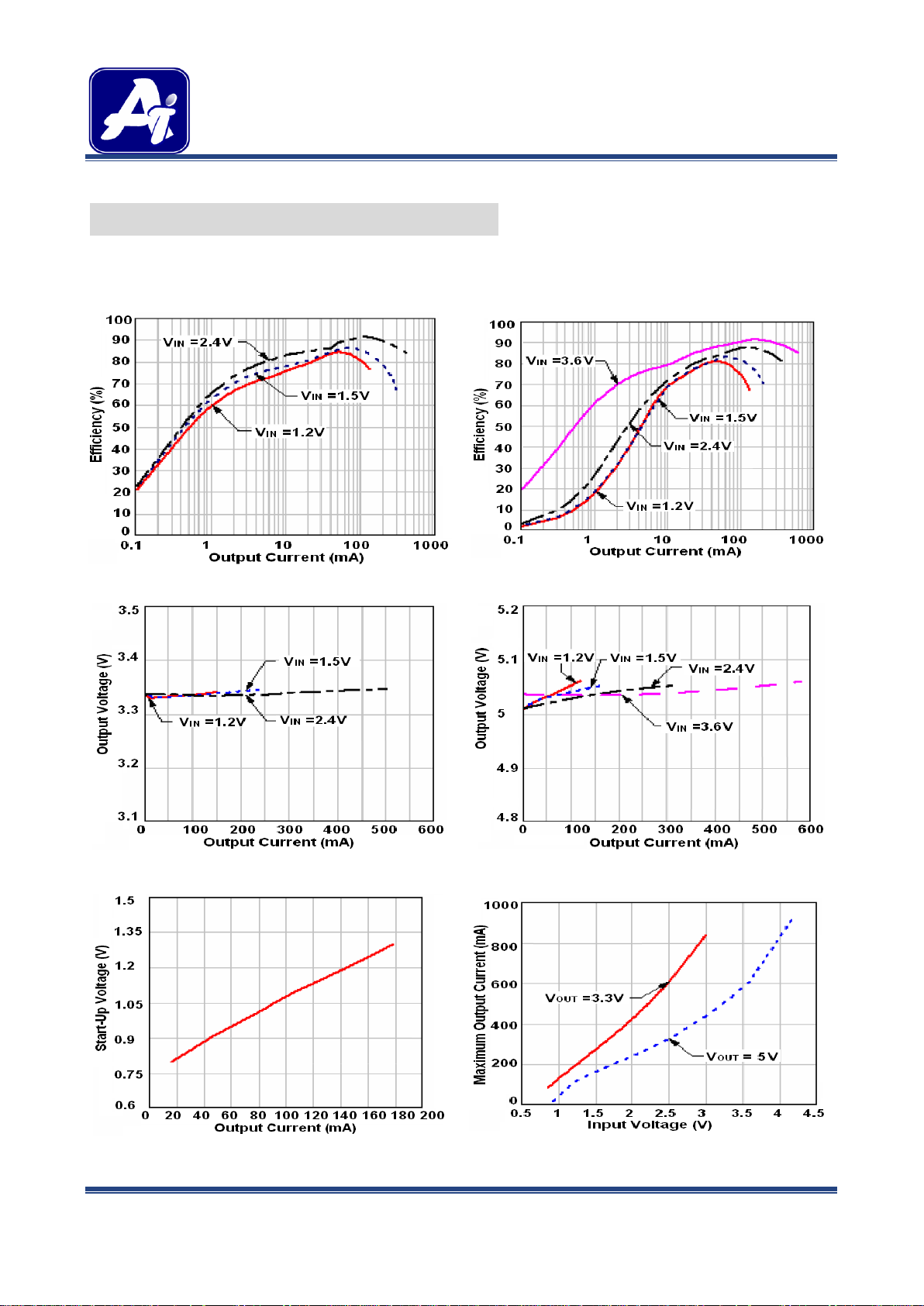
TYPICAL PERFORMANCE CHARACTERISTICS
1. Efficiency vs. Output Current
V
OUT
=3.3V, TA = 25°C
2. Input current vs. Output current
V
OUT
=5.0V, TA = 25°C
3. Output Voltage vs. Output Current
V
OUT
=3.3V, TA = 25°C
4. Output Voltage vs. Output Current
V
OUT
=5.0V, TA = 25°C
5. Minimum Start-Up Voltage vs. Output Current
V
OUT
=3.3V, TA = 25°C
6. Maximum Output Current vs. Input Voltage
L=4.7uH, TA = 25°C
REV1.0 - JAN 2012 RELEASE - - 5 -
 Loading...