

AiT A7221AE6R Schematic [ru]
AiT Semiconductor Inc.
www.ait-ic.com
A7221A
DESCRIPTION
FEATURES
to minimize the
ORDERING INFORMATION
Package Type
Part Number
A7221AE6R
A7221AE6VR
APPLICATION
TYPICAL APPLICATION
DC-DC CONVERTER BUC K (STEP-DOWN)
2A, 16V SYNCHRONOUS
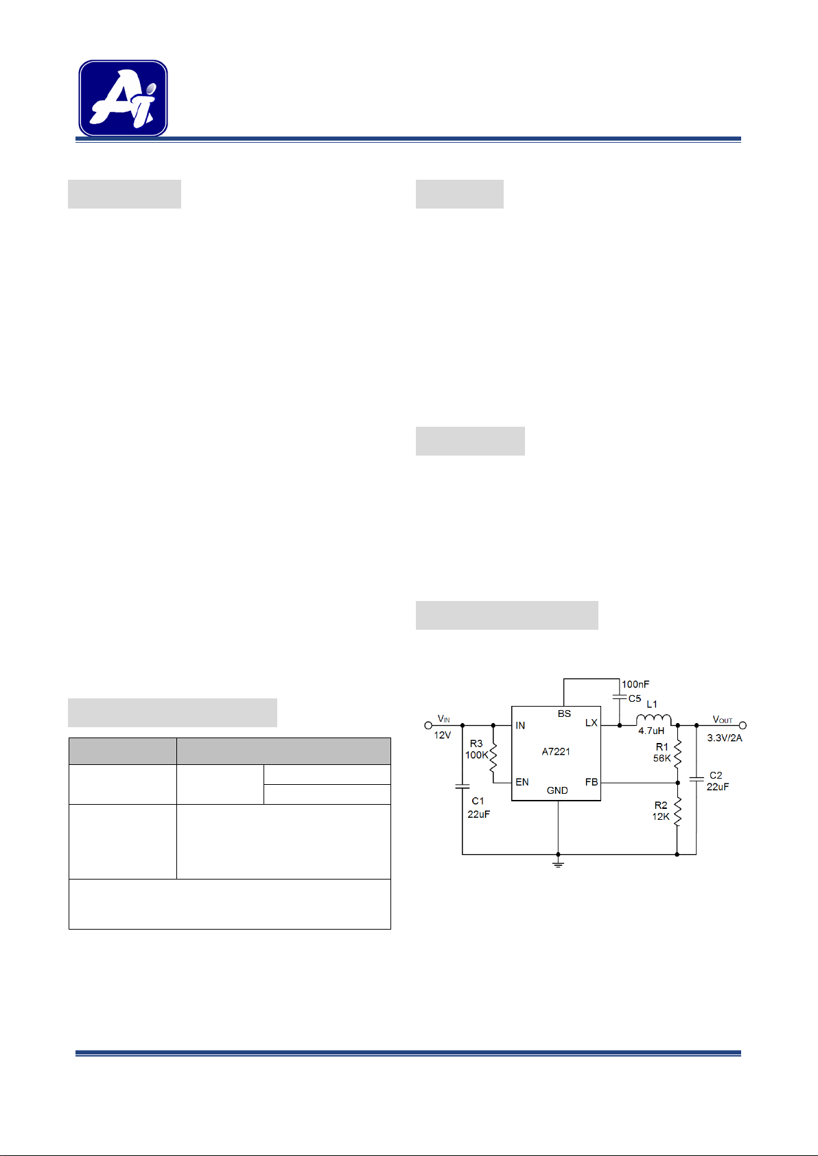
A7221A is simple, easy to use, 2A synchronous
step-down (Buck) convertor in SOT-26 package, with
high efficiency and fast transient response. A7221A
operates over a wide input voltage range from 4.5V to
16V and integrates main switch and synchronous
switch with very low R
DS(ON)
conduction loss. A7221A adopts the active constant
on time PWM architecture to achieve fast transient
responses for high step down applications and high
efficiency at light loads. In addition, it keeps in
constant frequency of 500kHz under heavy load
conditions to minimize the size of inductor and
capacitor. Fault conditions also include cycle-by-cycle
current limit, output under voltage protection, output
over current protection, output short-circuit protection
and thermal shutdown
Integrated 130mΩ and 120mΩ FETs
4.5~16V input voltage range
2A load current capability
Active constant on time PWM architecture with
500kHz switching frequency
Internal soft-start limits the inrush current
2% 0.6V reference
Available in SOT-26 Package
Set Top Box
Portable TV
Access Point Router
DSL Modem
LCD TV
The A7221A is available in SOT-26 package.
SOT-26 E6
V: Halogen free Package
Note
R: Tape & Reel
SPQ:3,000pcs/Reel
AiT provides all RoHS products
Suffix “ V “ means Halogen free Package
Figure 1. Typical Application Circuit
REV3.0 - DEC 2015 RELEASED, AUG 2016 UPDATED - - 1 -
AiT Semiconductor Inc.
www.ait-ic.com
A7221A
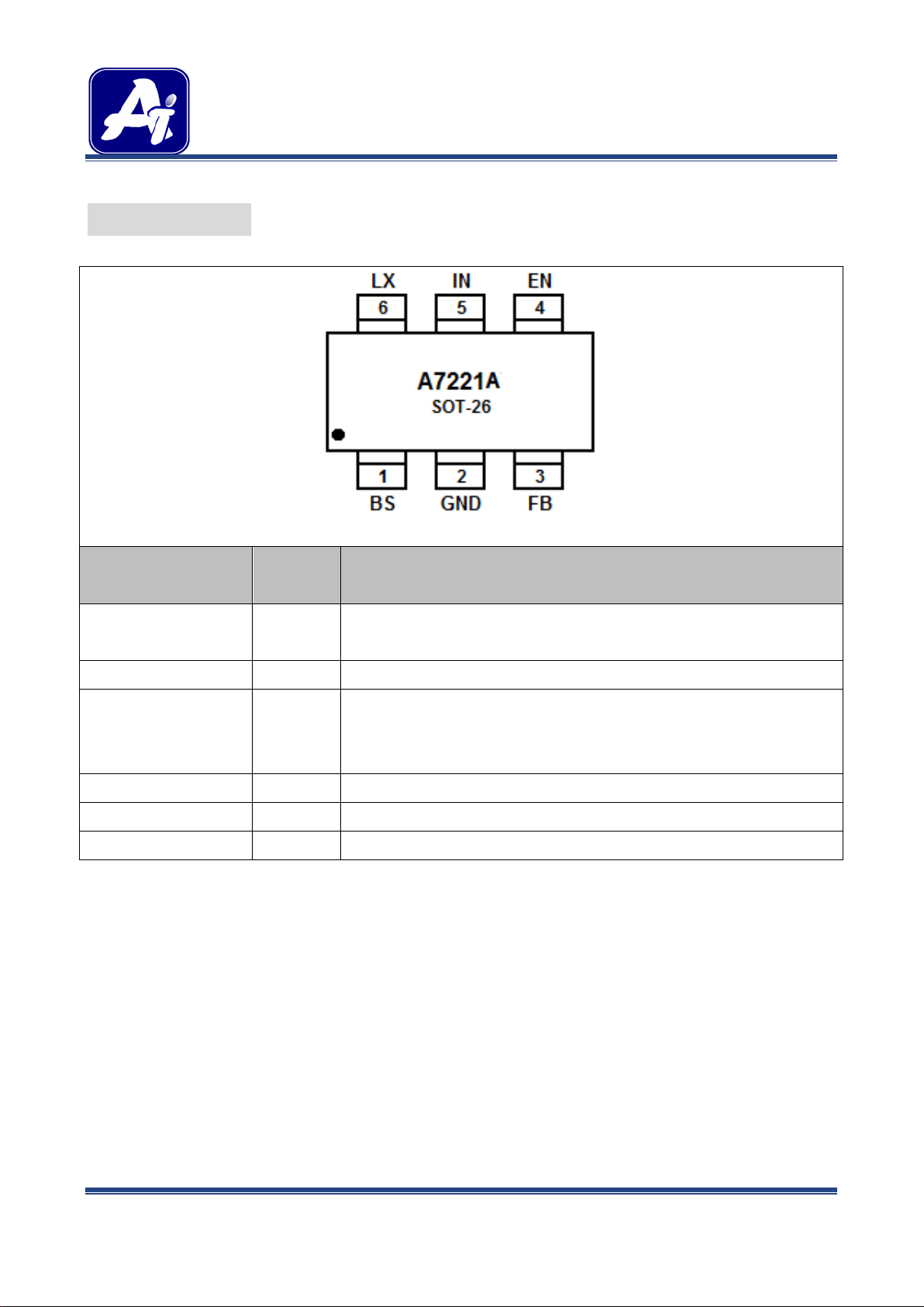
Pin #
Symbol
Function
PIN DESCRIPTION
DC-DC CONVERTER BUC K (STEP-DOWN)
2A, 16V SYNCHRONOUS
Top View
Boot-Strap Pin. Supply high side gate driver. Decouple this pin to LX
1 BS
pin with 0.1uF ceramic cap.
2 GND Ground pin.
Output Feedback Pin. Connect this pin to the center point of the output
3 FB
resistor divider (as shown in Figure 1) to program the output voltage:
V
=0.6x(1+R1/R2).
OUT
4 EN Enable control. Pull high to turn on. Do not float.
5 IN Input pin. Decouple this pin to GND pin with at least 1uF ceramic cap.
6 LX Inductor pin. Connect this pin to the switching node of inductor.
REV3.0 - DEC 2015 RELEASED, AUG 2016 UPDATED - - 2 -
AiT Semiconductor Inc.
www.ait-ic.com
A7221A
Parameter
Symbol
Min.
Max.
Unit
DC-DC CONVERTER BUC K (STEP-DOWN)
2A, 16V SYNCHRONOUS
ABSOLUTE MAXIMUM RATINGS
VIN, Supply Voltage -0.3V ~ 18V
VSW, Switch Voltage -1V ~ VIN + 0.3V
VEN, Enable -1V ~ VIN + 0.3V
VBS, Bootstrap Voltage -0.3V ~ +4V
VFB, Feedback Voltage -0.3V~ +4V
Thermal Resistance
θJA 100℃/W
θJC 55℃/W
Junction Temperature +150℃
Lead Temperature (Soldering, 10s) +260℃
NOTE1
Storage Temperature -65℃~+150℃
Stress beyond above listed “Absolute Maximum Ratings” may lead permanent damage to the device. These are stress ratings only and
operations of the device at these or any other conditions beyond those indicated in the operational sections of the specifications are not
implied. Exposure to absolute maximum rating conditions for extended periods may affect device reliability.
NOTE1: Measured on approximately 1” square of 1oz copper.
RECOMMENDED OPERATING CONDITIONS
NOTE2
Input Voltage VIN 4.5 16 V
Operating Temperature -40 85 ℃
NOTE2: The device is not guaranteed to function outside of its operating conditions.
REV3.0 - DEC 2015 RELEASED, AUG 2016 UPDATED - - 3 -
AiT Semiconductor Inc.
www.ait-ic.com
A7221A
Parameter
Conditions
Min.
Typ.
Max.
Unit
DC-DC CONVERTER BUC K (STEP-DOWN)
2A, 16V SYNCHRONOUS
ELECTRICAL CHARACTERISTICS
= 12V, V
V
IN
Shutdown Supply Current VEN=0V 10 20 μA
= 3.3V, L = 4.7uH, TA = 25°C, unless otherwise specified
OUT
Supply Current I
=0, VFB=V
OUT
×105% 350 μA
REF
Feedback Voltage 5V<VIN<16V 588 600 612 mV
FB Input Current -50 50 nA
High-Side Switch-On Resistance 130 mΩ
Low-Side Switch-On Resistance 120 mΩ
High-Side Switch Leakage VEN = 0V, VSW = 0V 0 10 μA
Upper Switch Current Limit 3.0 3.5 A
Lower Switch Current Limit 1.3 A
Oscillator Frequency 500 kHz
EN Rising Threshold 1.2 V
EN Falling Threshold 0.4 V
Input UVLO Threshold Rising VIN Rising 3.8 4.2 4.5 V
Input UVLO Threshold Hysteresis 15 mV
Min ON Time 50 ns
Soft-start Time tSS 0.2 ms
Max Duty Cycle 85 %
Thermal Shutdown 160 ℃
REV3.0 - DEC 2015 RELEASED, AUG 2016 UPDATED - - 4 -
AiT Semiconductor Inc.
www.ait-ic.com
A7221A
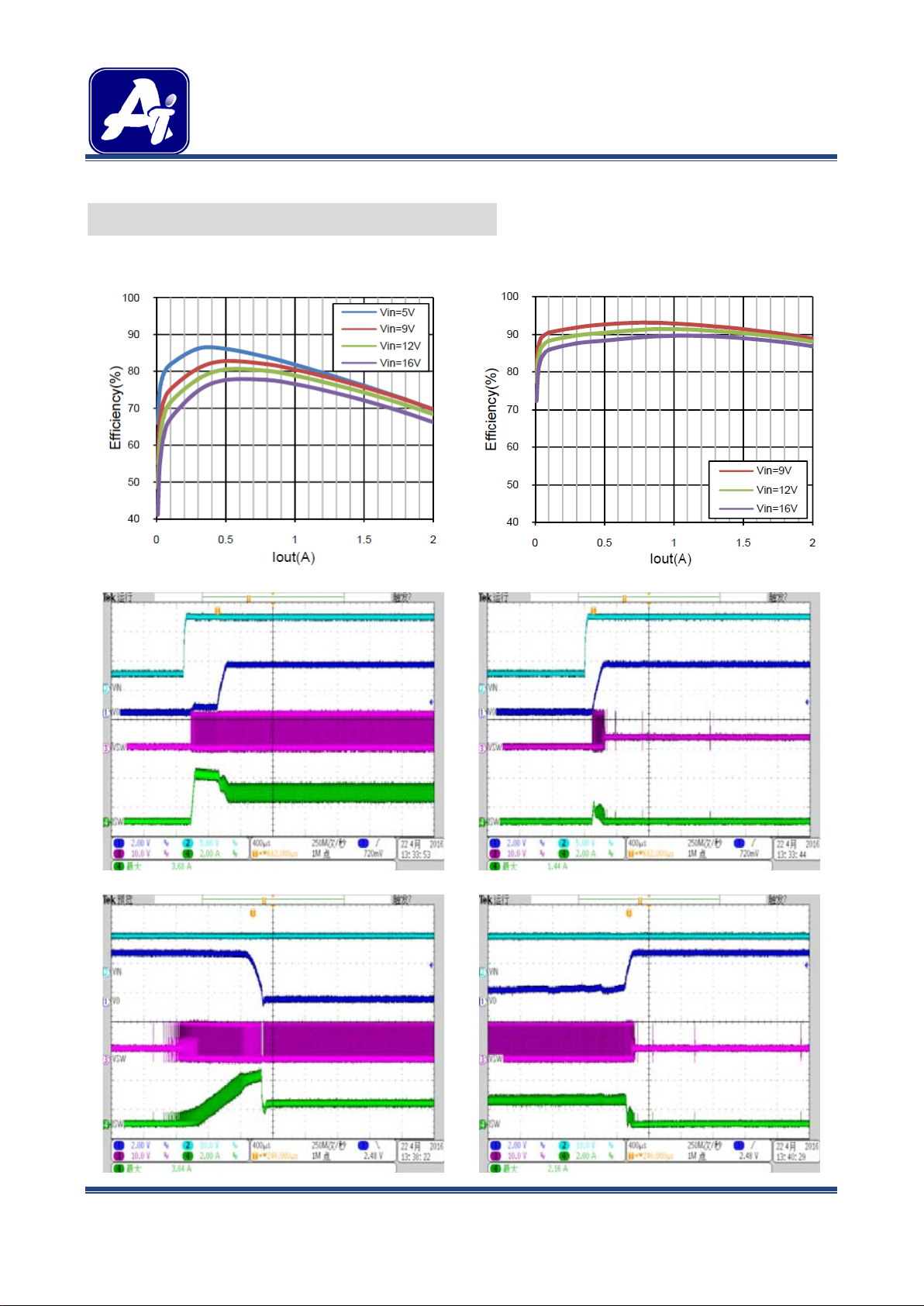
1. Efficiency vs. I
OUT
@V
OUT
=1.2V
2. Efficiency vs. I
OUT
@V
OUT
=5V
3. Soft-Start (V
IN
=12V, VO=3.3V, IO=2A)
4. Soft-Start (V
IN
=12V,VO=3.3V,IO=0A)
5. Short Circuit
6. Short Circuit Recovery
TYPICAL PERFORMANCE CHARACTERISTICS
DC-DC CONVERTER BUC K (STEP-DOWN)
2A, 16V SYNCHRONOUS
REV3.0 - DEC 2015 RELEASED, AUG 2016 UPDATED - - 5 -
 Loading...