

AiT A7122AE5R, A7122AE6R Schematic [ru]
AiT Semiconductor Inc.
www.ait-ic.com
A7122A
DESCRIPTION
FEATURES
overload protection improves design
ORDERING INFORMATION
Package Type
Part Number
APPLICATION
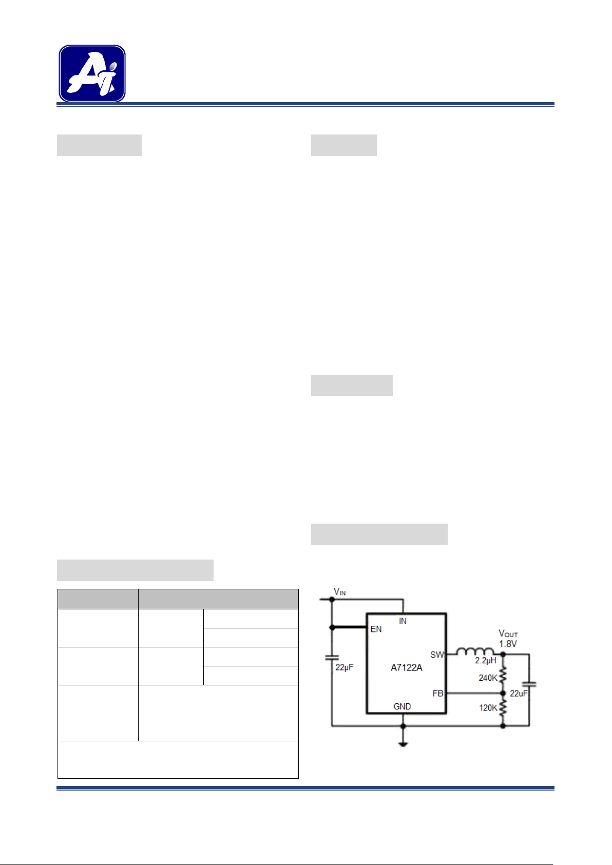
TYPICAL APPLICATION
DC-DC CONVERTER BUCK (STEP-DOWN)
5.5V 2A 1.3MHz SYNCHRONOUS
The A7122A is a high-efficiency, DC-to-DC
step-down switching regulators, capable of delivering
up to 2A of output current. The device operates from
an input voltage range of 2.5V to 5.5V and provides
an output voltage from 0.6V to V
, making the
IN
A7122A ideal for low voltage power conversions.
Running at a fixed frequency of 1.3MHz allows the
use of small external components, such as ceramic
input and output caps, as well as small inductors,
while still providing low output ripples. This low noise
output along with its excellent efficiency achieved by
the internal synchronous rectifier, making A7122A an
ideal green replacement for large power consuming
linear regulators. Internal soft-start control circuitry
reduces inrush current. Short-circuit and
thermal-
reliability.
High Efficiency: Up to 97%
Capable of Delivering 2A
1.3MHz Switching Frequency
No External Schottky Diode Needed
Light-load Mode
Internal Compensation and Soft-Start
Current Mode control
0.6V Reference for Low Output voltages
Logic Control Shutdown (I
<1uA)
Q
Thermal shutdown and UVLO
Available in SOT-26 and SOT-25 Packages
Digital Cameras
MP3 and MP4 players
Set top boxes
Wireless and DSL Modems
The A7122A is available in SOT-26 and SOT-25
packages.
SOT-26 E6
SOT-25 E5
V: Halogen free Package
Note
AiT provides all RoHS products
Suffix “ V “ means Halogen free Package
R: Tape & Reel
SPQ: 3,000pcs/Reel
USB supplied Devices in Notebooks
Portable Devices
A7122AE6R
A7122AE6VR
A7122AE5R
A7122AE5VR
REV1.0 - MAY 2016 RELEASED - - 1 -
AiT Semiconductor Inc.
www.ait-ic.com
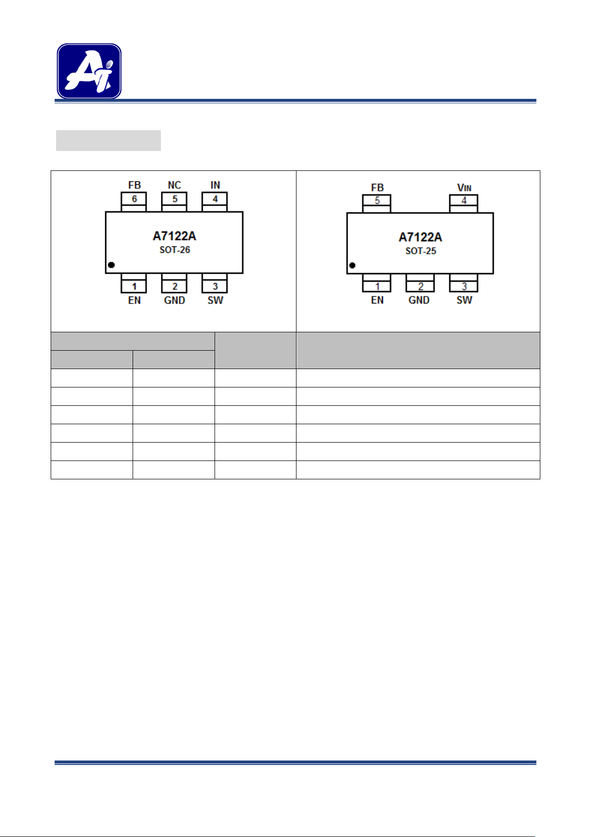
A7122A
Pin #
Symbol
Function
SOT-26
SOT-25
PIN DESCRIPTION
DC-DC CONVERTER BUCK (STEP-DOWN)
5.5V 2A 1.3MHz SYNCHRONOUS
Top View
1 1 EN Enable pin
2 2 GND Ground
3 3 SW Power Switch Output
4 4 IN Power Supply Input
5 - NC Not Connected
6 5 FB Feedback input pin
Top View
REV1.0 - MAY 2016 RELEASED - - 2 -

AiT Semiconductor Inc.
www.ait-ic.com
A7122A
Parameter
Symbol
Min
Max
Unit
DC-DC CONVERTER BUCK (STEP-DOWN)
5.5V 2A 1.3MHz SYNCHRONOUS
ABSOLUTE MAXIMUM RATINGS
Max Input Voltage 6.5V
TJ, Max Operating Junction Temperature 125°C
TA, Ambient Temperature -40°C ~ 85°C
Maximum Power Dissipation SOT-25 400mW
TS, Storage Temperature -40°C ~ 150°C
Lead Temperature & Time 260°C, 10s
Stress beyond above listed “Absolute Maximum Ratings” may lead permanent damage to the device. These are stress ratings only and
operations of the device at these or any other conditions beyond those indicated in the operational sections of the specifications are not
implied. Exposure to absolute maximum rating conditions for extended periods may affect device reliability.
RECOMMENDED OPERATING CONDITIONS
VIN Supply Voltage
Operating Temperature
V
2.5 5.5 V
IN
T
-40 85 ℃
OPT
REV1.0 - MAY 2016 RELEASED - - 3 -
AiT Semiconductor Inc.
www.ait-ic.com
A7122A
Parameter
Symbol
Conditions
Min.
Typ.
Max.
Unit
DC-DC CONVERTER BUCK (STEP-DOWN)
5.5V 2A 1.3MHz SYNCHRONOUS
ELECTRICAL CHARACTERISTICS
=5V, TA=25°C
V
DD
Input Voltage Range VIN 2.5 5.5 V
Feedback Voltage VFB 0.585 0.6 0.615 V
Feedback Leakage Current IFB 0.1 0.4 μA
Quiescent Current IQ Active, VFB=0.65V 50 μA
Shutdown Current ISD Shutdown 1 μA
Switching Frequency FSW 1.3 MHz
PMOSFET R
NMOSFET R
Peak Current Limit I
SW Leakage Current ISW
R
DSON
R
DSON
120 mΩ
ONP
80 mΩ
ONN
2.5 A
LIMIT
V
=5.5V,VSW=0 or 5.5V,
IN
10 μA
V
=0V
EN
EN Leakage Current IEN 1 μA
EN Input High Voltage V
EN Input Low Voltage V
1.5 V
ENH
0.4 V
ENL
Thermal Shutdown TSD 150 ℃
Thermal Shutdown Hysteresis HYSTSD 15 ℃
REV1.0 - MAY 2016 RELEASED - - 4 -
AiT Semiconductor Inc.
www.ait-ic.com
A7122A
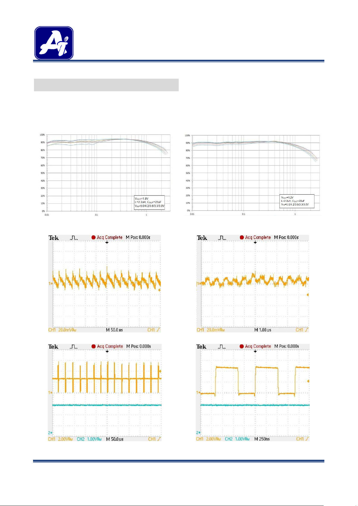
TYPICAL OPERATING CHARACTERISTICS
Tested under T
1. 2.
=25°C, unless otherwise specified
A
DC-DC CONVERTER BUCK (STEP-DOWN)
5.5V 2A 1.3MHz SYNCHRONOUS
3. 4.
5. 6.
REV1.0 - MAY 2016 RELEASED - - 5 -
 Loading...