

AiT A6155E6R Schematics
AiT Semicond
AiT Semiconductor Inc.
AiT SemicondAiT Semicond
www.ait-ic.com
DESCRIPTION
DESCRIPTION FEATURES
DESCRIPTIONDESCRIPTION
uctor Inc.
uctor Inc.uctor Inc.
FEATURES
FEATURESFEATURES
AAAA6155
6155
61556155
LOW DROPOUT VOLTAGE REGULATOR
150mA DUAL OUTPUT CMOS LOW NOISE
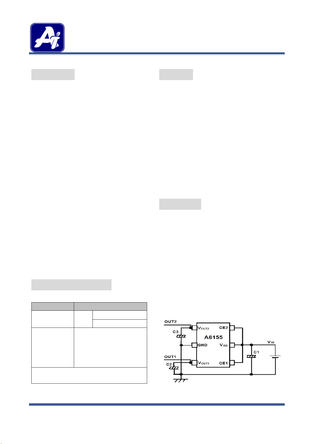
The A6155 is a dual output, low noise; low-dropout
regulator delivers at least 150mA of continuous
output current. The output voltage for each
regulator is set independently by trimming.
Voltages are selectable in 100mV steps within a
range of 1.2V to 5.0V. Typical output noise is
27uV
The A6155 includes two independent
logic-controlled shutdown inputs and allows the
output of each regulator to be turned of
independently.
The A6155 includes high accuracy voltage
reference, error amplifier, and current limit circuit
and output driver module.
The A6155 has excellent load and line transient
response and good temperature characteristics,
which can assure the stability of chip and power
system and A6155 uses trimming technique to
guarantee output voltage accuracy within ±2%.
The A6155 is available in SOT-26 package.
ORDERING INFORMATION
ORDERING INFORMATION
ORDERING INFORMATIONORDERING INFORMATION
AiT provides all Pb free products
Suffix “ V “ means Green Package
, and PSRR is 65dB at 1KHz.
RMS
Package Type
Package Type
Package TypePackage Type
SOT-26 E6
X: Output Portfolio
See output voltage portfolio
Note
Z: Pin Type, C or D
V: Green Package
R: Tape & Reel
Part Number
Part Number
Part NumberPart Number
A6155E6R-XZ
A6155E6VR-XZ
Low Output Noise (27uV
Standby Mode: 0.1uA
150mA output current for each channel
25uA Operating Supply Current per channel
High Ripple Rejection: 65dB@1KHz(Typ.)
Low 200mV dropout at 100mA load
Excellent Line Regulation: 0.05%/V
Built-in chip Enable Circuit
Independent Shutdown Controls
Output Voltage Range: 1.2V~5.0V
Output Current Limit
Highly Accurate: ±2% (±1% customized)
Available in SOT-26 Package
APPLICATION
APPLICATION
APPLICATIONAPPLICATION
Power Source for Cellular Phones and various
kind of PCs
Battery Powered Equipment
Power Management of MP3, PDA, DSC,
Mouse, PS2 Games
Reference Voltage Source
Regulation after Switching Power
Notebook and Handheld equipment
Wireless LAN, Bluetooth, GPS Receivers
Cordless Phones
Radio Communication Equipment
Typical
Typical Application
Typical Typical
Application
ApplicationApplication
RMS
)
REV1.2 - DEC 2006 RELEASED – DEC 2008 REVISED - - 1 -

AiT Semicond
AiT Semiconductor Inc.
AiT SemicondAiT Semicond
www.ait-ic.com
PIN DESCRIPTION
PIN DESCRIPTION
PIN DESCRIPTIONPIN DESCRIPTION
uctor Inc.
uctor Inc.uctor Inc.
AAAA6155
6155
61556155
LOW DROPOUT VOLTAGE REGULATOR
150mA DUAL OUTPUT CMOS LOW NOISE
Pin #
Pin # Symbol
Pin #Pin #
Type C
Type C Type D
Type CType C
1 6 V
2 2 VDD Input Pin
3 4 V
4 3 CE2 Chip Enable Pin2
5 5 GND Ground Pin
6 1 CE1 Chip Enable Pin1
Top View
Type D
Type DType D
Top View
Symbol Function
SymbolSymbol
Output1 Pin
OUT1
Output2 Pin
OUT2
Function
FunctionFunction
REV1.2 - DEC 2006 RELEASED – DEC 2008 REVISED - - 2 -
AAAA6155
6155
AiT Semicond
AiT Semiconductor Inc.
AiT SemicondAiT Semicond
www.ait-ic.com
OUTPUT VOLTAGE PORTFOLIO
OUTPUT VOLTAGE PORTFOLIO
OUTPUT VOLTAGE PORTFOLIOOUTPUT VOLTAGE PORTFOLIO
Output Voltage
Output Voltage Part Number
Output VoltageOutput Voltage
Code
Code
CodeCode
A 1.5 2.5 A6155E6-AC A6155E6-AD M 2.8 1.8 A6155E6-MC A6155E6-MD
B 1.5 2.8 A6155E6-BC A6155E6-BD N 2.8 2.5 A6155E6-NC A6155E6-ND
C 1.5 3.0 A6155E6-CC A6155E6-CD
D 1.5 3.3 A6155E6-DC A6155E6-DD
E 1.5 4.0 A6155E6-EC A6155E6-ED Q 3.0 2.5 A6155E6-QC A6155E6-QD
F 1.8 1.8 A6155E6-FC A6155E6-FD R 3.0 3.0 A6155E6-RC A6155E6-RD
G 1.8 2.5 A6155E6-GC A6155E6-GD
H 1.8 2.8 A6155E6-HC A6155E6-HD
I 1.8 3.0 A6155E6-IC A6155E6-ID U 3.3 2.5 A6155E6-UC A6155E6-UD
J 1.8 3.3 A6155E6-JC A6155E6-JD V 3.3 2.8 A6155E6-VC A6155E6-VD
K 2.5 1.8 A6155E6-KC A6155E6-KD W 3.3 3.3 A6155E6-WC A6155E6-WD
L 2.5 2.5 A6155E6-LC A6155E6-LD X 2.8 1.5 A6155E6-XC A6155E6-XD
VVVV
VVVV
1111
2222
Type C
Type C Type D
Type CType C
uctor Inc.
uctor Inc.uctor Inc.
Part Number Output Voltage
Part NumberPart Number
Type D Code
Type DType D
Output Voltage PPPPaaaart Number
Output VoltageOutput Voltage
Code
CodeCode
O 2.8 2.8 A6155E6-OC A6155E6-OD
P 2.8 3.0 A6155E6-PC A6155E6-PD
S 3.0 3.3 A6155E6-SC A6155E6-SD
T 3.3 1.8 A6155E6-TC A6155E6-TD
VVVV
1111
LOW DROPOUT VOLTAGE REGULATOR
150mA DUAL OUTPUT CMOS LOW NOISE
rt Number
rt Numberrt Number
VVVV
2222
Type C
Type C Type D
Type CType C
61556155
Type D
Type DType D
ABSOLUTE MAXIMUM RATINGS
ABSOLUTE MAXIMUM RATINGS
ABSOLUTE MAXIMUM RATINGSABSOLUTE MAXIMUM RATINGS
Max Input Voltage 10V
Junction Temperature(TJ) 125oC
Output Current 200mA
Power Dissipation (SOT-26) 200mW
Storage Temperature (Ts) -45oC~150oC
Lead Temperature and Time 260oC, 10S
Stresses beyond may cause permanent damage to the device. These are stress ratings only and functional operation of the device at
these or any other conditions beyond those indicated in the Electrical Characteristics are not implied. Exposure to absolute maximum
rating conditions for extended periods may affect device reliability.
REV1.2 - DEC 2006 RELEASED – DEC 2008 REVISED - - 3 -
AiT Semicond
AiT Semiconductor Inc.
AiT SemicondAiT Semicond
www.ait-ic.com
ELECTRICAL CHARACTERISTICS
ELECTRICAL CHARACTERISTICS
ELECTRICAL CHARACTERISTICSELECTRICAL CHARACTERISTICS
uctor Inc.
uctor Inc.uctor Inc.
LOW DROPOUT VOLTAGE REGULATOR
150mA DUAL OUTPUT CMOS LOW NOISE
Test Conditions: C1=1uF, C2=C3==2.2uF, TA=25oC, unless otherwise specified.
Symbol
Symbol Parameter
SymbolSymbol
Parameter Conditions
ParameterParameter
Conditions Min
ConditionsConditions
Min Typ
MinMin
VIN Input Voltage 1.5 8 V
V
Output Voltage VIN=Set V
OUT
I
(Max) Max Output Current VIN-V
OUT
Dropout
Voltage
ΔV
ΔV
IN
ΔV
OUT
OUT
x V
/ΔI
OUT
OUT
Input-Output Voltage
Differential
Line Regulation I
Load Regulation VIN=Set V
Iss Supply Current VIN=Set V
I
STANDBY
Supply Current (Standby) VIN=Set V
1mA≦I
OUT
Refer to the Electrical Characteristics by output voltage
=40mA
OUT
1.6V≦Vin≦8V
1mA≦I
OUT
+1V
OUT
≦30mA
V
OUT
x0.98
=1V 150 mA
0.05
+1V
OUT
≦80mA
OUT
+1V 25 50 uA
OUT
+1V,
OUT
12 40 mV
0.1 1.0 uA
VCE=GND
ΔV
OUT
ΔT x V
OUT
PSRR Ripple Rejection F=1KHz,
Output Voltage
Temperature Coefficiency
I
=30mA ±100
OUT
65 dB
Ripple=0.5Vp-p
I
Short Current Limit V
LIM
VIN=Set V
=0V 20 mA
OUT
OUT
+1V
Rpd CE Pull down Resistance 2.0 5.0 10.0 mΩ
V
CE Input Voltage “H” 1.5 VIN V
CEH
V
CE Input Voltage “L” 0 0.25 V
CEL
en Output Noise BW=10Hz~100KHz 27 uV
Typ Max
TypTyp
V
Max Unit
MaxMax
OUT
x1.02
0.2 %/V
ppm/oC
AAAA6155
6155
61556155
Unit
UnitUnit
V
RMS
ELECTRICAL CHARACTERISTICS BY OUTPUT VOLTAGE
ELECTRICAL CHARACTERISTICS BY OUTPUT VOLTAGE
ELECTRICAL CHARACTERISTICS BY OUTPUT VOLTAGEELECTRICAL CHARACTERISTICS BY OUTPUT VOLTAGE
Output Voltage
Output Voltage
Output VoltageOutput Voltage
VVVV
(V)
(V)
(V)(V)
OUT
OUT
OUTOUT
V
=1.5V
OUT
V
=1.6V 0.36 0.65
OUT
V
=1.7V 0.34 0.60
OUT
1.8V≦V
2.1V≦V
2.8V≦V
REV1.2 - DEC 2006 RELEASED – DEC 2008 REVISED - - 4 -
≦2.0 0.32 0.55
OUT
≦2.7 0.28 0.60
OUT
≦4.0 0.22 0.35
OUT
Condition
Condition Typ.
ConditionCondition
I
=120mA
OUT
Dropout Voltage, V
Dropout Voltage, V
Dropout Voltage, VDropout Voltage, V
Typ. Max
Typ.Typ.
0.38 0.70
DIF
DIF
DIFDIF
(V)
(V)
(V)(V)
Max
MaxMax
 Loading...