

AIM AT1382A Datasheet
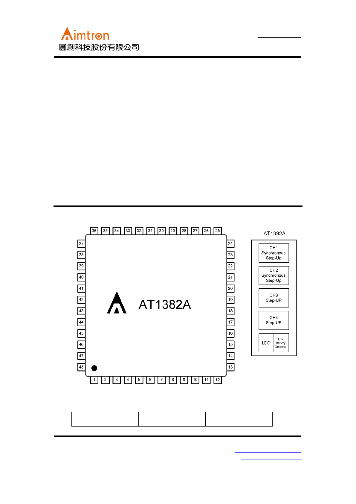
AT1382A
4-Channel DC-DC Converter for DSC
Features
• Low start-up power supply voltage :1.4V(CH4)
• Wide supply voltage range from 1.8V to 7V
(CH1~4)
• High speed operation is possible: Maximum
1 MHz
• Supports for up, flyback and up/down SEPIC
conversion (CH1~4)
• Totem-pole type output for MOSFET
• Built-in On/Off function
• Built-in Short-Circuit Protection.
Applications
• Digital Cameras
• CCD Imaging Devices
• Camcorders
General Description
The AT1382A is a 4-channel PWM DC/DC control
IC for low voltage applications with a soft start
function and short circuit detection function. This
IC is ideal for up conversion, down conversion,
and up/down conversion (using a step-up/stepdown SEPIC system with free input and output
settings). Four channels can be built in the
LQFP48 package, each channel be controlled, and
soft-start.
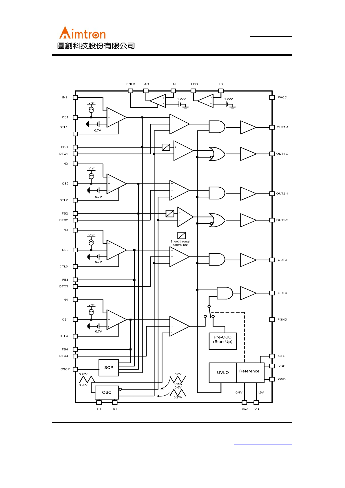
The AT1382A include one comparator to generate
low-battery warning outputs. It also contains a gain
block that can be used with an external P-channel
MOSFET to make a low-dropout linear regulator.
Pin Assignment
Ordering Information
Part number Package Marking
AT1382A LQFP48 AT1382AF
2F, No.10, Prosperity RD. II, Science-Based Industrial Park, Hsinchu 300,Taiwan, R.O.C.
Tel: 886-3-563-0878 WWW: http://www.aimtron.com.tw
Fax: 886-3-563-0879 Email: service@aimtron.com.tw
1
AT1382A
4-Channel DC-DC Converter for DSC
Pin Description
Pin No. Pin name I/O Function
1 DTC4 I CH4 Dead Time Control
2 FB4 O CH4 Error Amplifier Output
3 IN4 I CH4 Error Amplifier Inverted Input
4 CS4 - CH4 Soft Start Setting Capacitor
5 CTL4 I CH4 ON/OFF Control
6 DTC3 I CH3 Dead Time Control
7 FB3 O CH3 Error Amplifier Output
8 IN3 I CH3 Error Amplifier Inverted Input
9 CS3 - CH3 Soft Start Setting Capacitor
10 CTL3 I CH3 ON/OFF Control
11 CSCP - Timer Latch Short-Circuit Detection Capacitor Input
12 VREF O Reference 0.9V Output
13 GND P Ground
14 GND P Ground
15 VBG TEST Reference Test Pin
16 VCC P Power Supply
17 VCC P Power Supply
18 POR TEST Pre-OSC Change to Main-OSC Indicator
19 RT - Oscillation Frequency Setting Resistor
20 CT - Oscillation Frequency Setting Capacitor
21 VB O Reference 1.8V Output
22 CTL I Power Supply Control
23 ENLD I Gain Block Enable Input
24 CT2 TEST Triangular wave OSC Inverted output Test Pin
25 CTL2 I CH2 ON/OFF Control
26 CS2 - CH2 Soft Start Setting Capacitor
27 IN2 I CH2 Error Amplifier Inverted Input
28 FB2 O CH2 Error Amplifier Output
29 DTC2 I CH2 Dead Time Control
30 CTL1 I CH1 ON/OFF Control
31 CS1 - CH1 Soft Start Setting Capacitor
32 IN1 I CH1 Error Amplifier Inverted Input
33 FB1 O CH1 Error Amplifier Output
34 DTC1 I CH1 Dead Time Control
35 LBI I Low Battery Detected Input
36 LBO O Low Battery Indicator
37 AI I LDO Regulated Input
38 AO O LDO Drive Output
39 OUT1_1 O CH1 Main Side Output
40 OUT1_2 O CH1 Synchronous Rectifier Side Output
41 OUT2_1 O CH2 Main Side Output
42 OUT2_2 O CH2 Synchronous Rectifier Side Output
43 N.C. 44 PVCC P Drive Output Block Power Supply
45 N.C. 46 PGND P Drive Output Block Ground
47 OUT3 O CH3 Output
48 OUT4 O CH4 Output
2F, No.10, Prosperity RD. II, Science-Based Industrial Park, Hsinchu 300,Taiwan, R.O.C.
Tel: 886-3-563-0878 WWW: http://www.aimtron.com.tw
Fax: 886-3-563-0879 Email: service@aimtron.com.tw
2
AT1382A
4-Channel DC-DC Converter for DSC
Block Diagram
2F, No.10, Prosperity RD. II, Science-Based Industrial Park, Hsinchu 300,Taiwan, R.O.C.
Tel: 886-3-563-0878 WWW: http://www.aimtron.com.tw
Fax: 886-3-563-0879 Email: service@aimtron.com.tw
3
AT1382A
g
yp
4-Channel DC-DC Converter for DSC
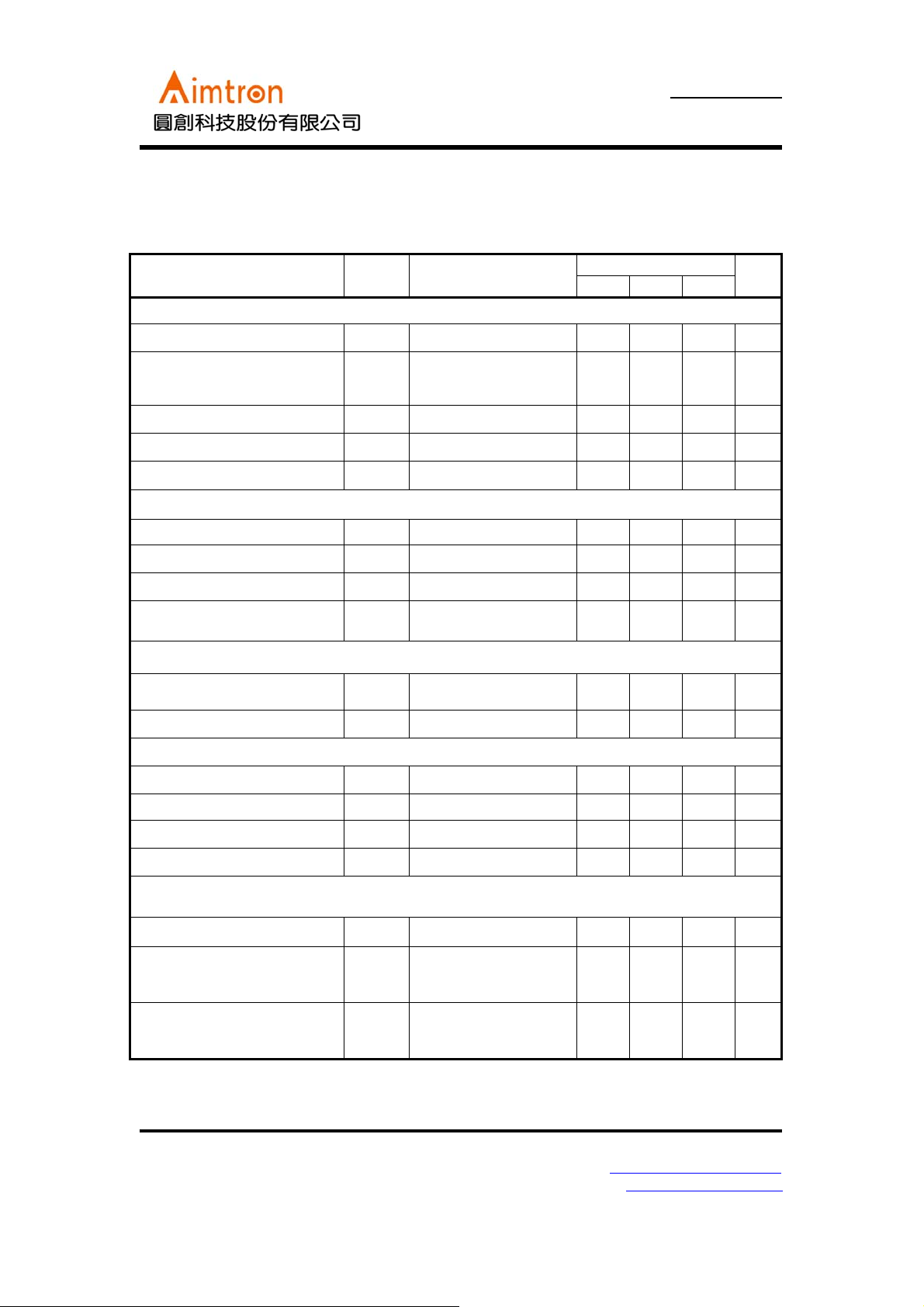
Absolute Maximum Ratings
Parameter Symbol Condition
Ratin
Min Max
Unit
Power supply voltage Vcc -- -- 8 V
Output current Io Output pin -- 20 mA
Output peak current Io
Power dissipation P
Operation temperature Topr -- -30 85
Storage temperature Tstg -- -55 125
Semiconductor devices can be permanently damaged by application of stress in excess of absolute ratings. Do not
*
exceed these ratings.
Output pin, Duty≦5%
Ta≦25℃ (LQFP-48P)
D
-- 200 mA
-- 860 mW
℃
℃
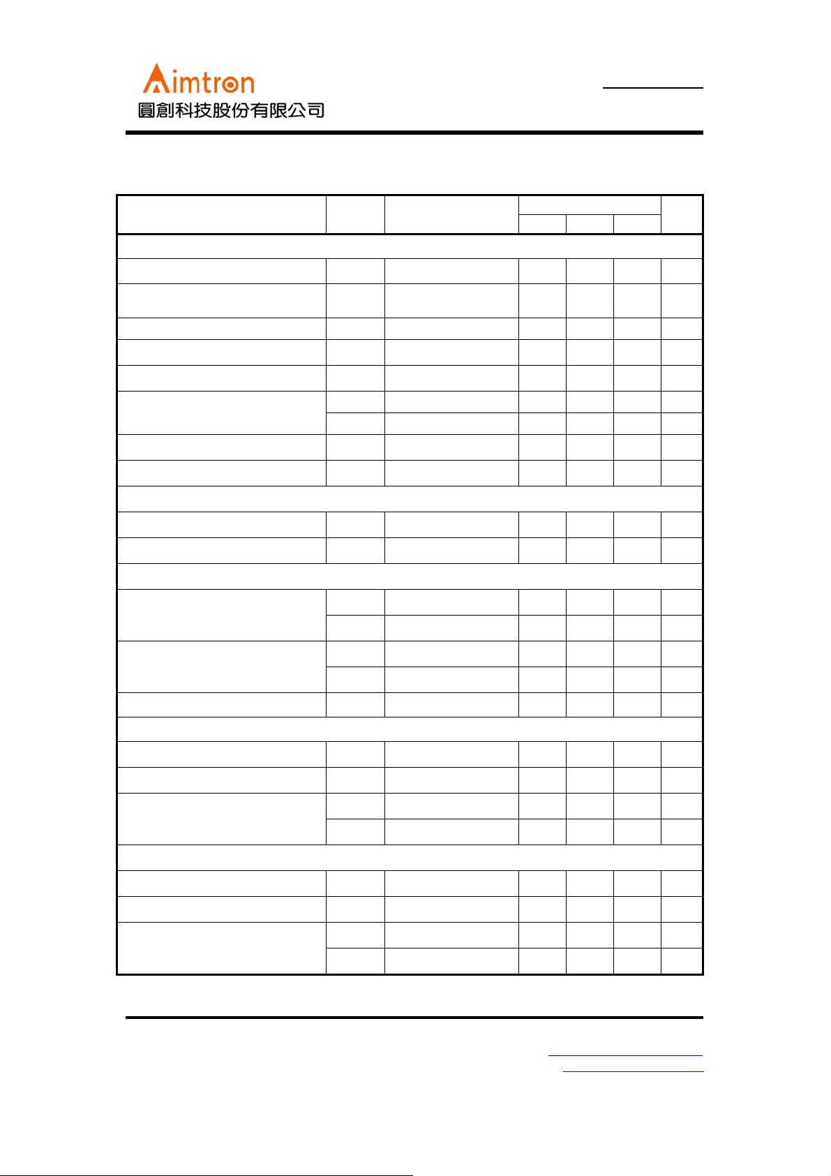
Recommended Operating Conditions
Val ue
Parameter Symbol Condition
Min T
Startup power supply voltage Vcc CH4 1.4 -- 7 V
Power supply voltage Vcc
Reference voltage output current I
VB pin output current I
Input voltage V
Control input voltage V
Output current Io
Oscillator f
Timing capacitor C
Timing resistor R
Soft start capacitor
C
Short detection capacitor C
VB pin capacitor C
Operating ambient temperature Ta -- -30 25 85
CH4 1.5 5.0 7 V
CH1 to CH3 1.8 5.0 7 V
VREF pin -1 -- 0 mA
OR
VB pin -0.5 -- 0 mA
B
IN1 to IN4 pins 0 -- Vcc-1.8 V
IN
CTL pin 0 -- 7 V
CTL
OUT pin (CH1 to CH3) -- 2 15 mA
OUT pin (CH4) 1 2 15 mA
OSC
T
T
-- 100 500 1000 kHz
-- 47 100 560 pF
-- 8.2 18 100
Cs CH1 to CH3 -- 0.027 1.0
CH4 -- 0.47 1.0
+IN6
SCP
VB
-- -- 0.1 1.0
-- 0.082 0.1 --
Max
Unit
kΩ
μF
μF
μF
μF
℃
2F, No.10, Prosperity RD. II, Science-Based Industrial Park, Hsinchu 300,Taiwan, R.O.C.
Tel: 886-3-563-0878 WWW: http://www.aimtron.com.tw
Fax: 886-3-563-0879 Email: service@aimtron.com.tw
4
AT1382A
4-Channel DC-DC Converter for DSC
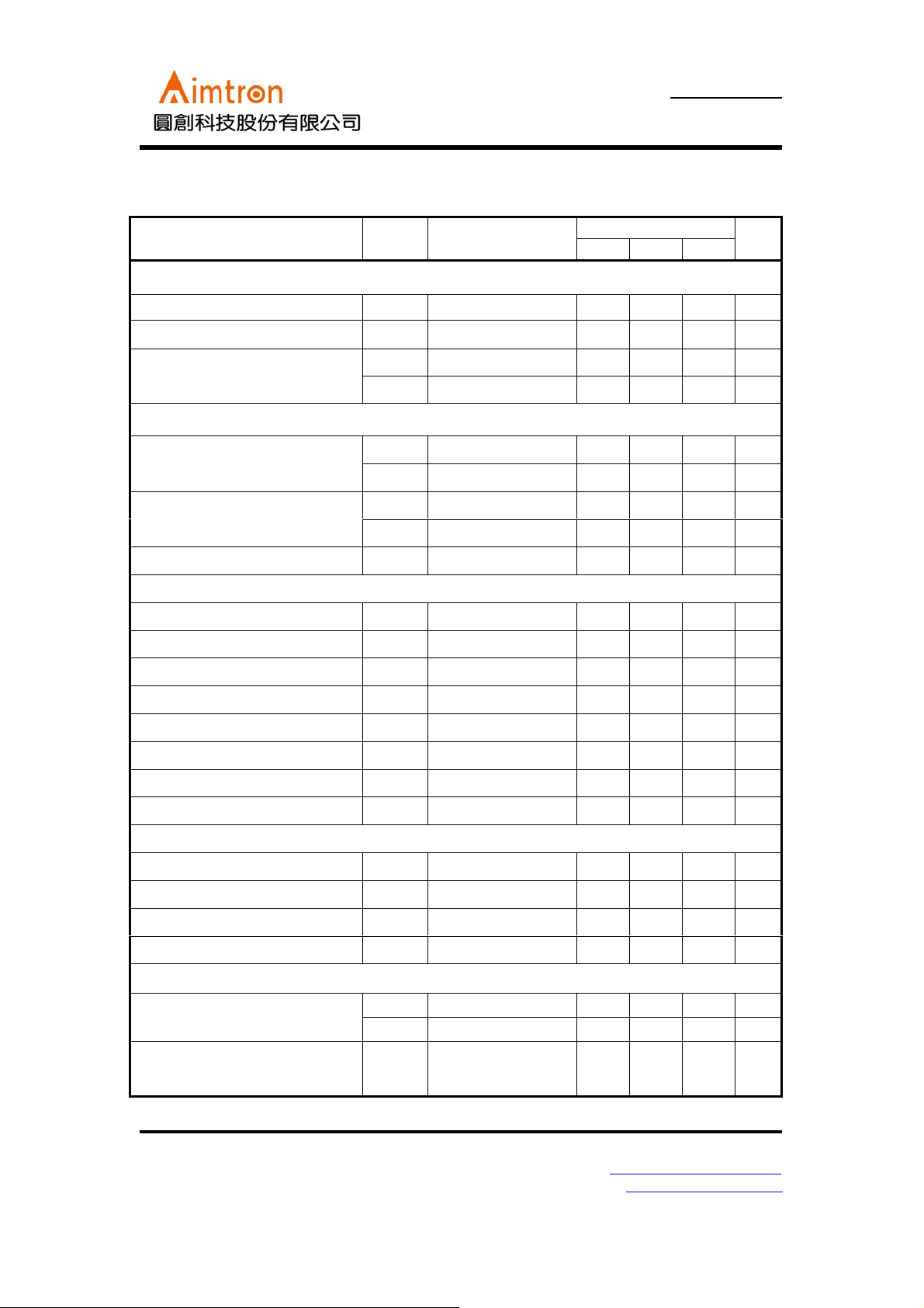
Electrical Characteristics
(Ta=25℃, VCC=PVCC=5V)
Parameter Symbol Condition
Reference voltage block [REF]
Measure result
Min. Typ. Max.
Unit
Reference voltage V
Output voltage temperature
△V
stability
/V
REF
REF
Ta = -30℃ to 85℃
REF
0.88 0.90 0.92 V
-0.5-%
Input stability Line VCC=1.8V to 7V -10 - 10 mV
Load stability Load VREF=0mA to –1mA -10 - 10 mV
Shout circuit output current I
VREF=0.7V -20 -5 -1 mA
OSC
Under voltage lockout block [U.V.L.O]
Threshold voltage(CH1~CH3) V
Hysteresis width(CH1~CH3) V
Reset voltage(CH1~CH3) V
CH4 Pre-OSC change to MainOSC threshold
V
TH
H
RST
TH2
1.5 1.6 1.7 V
-0.2-V
1.6 1.7 1.8 V
-1.7-V
Soft start block [CS]
Input standby voltage V
Charge current I
STB
CS
-50100mV
-6.0 -5.0 -4.0
μA
Short circuit detection block [SCP]
Threshold voltage V
Input standby voltage V
Input latch voltage V
Input source current I
TH
STB
I
CSCP
0.65 0.70 0.75 V
-50100mV
-50100mV
-1.4 -1.0 -0.6
μA
Triangular wave oscillator block [OSC]
Oscillator frequency f
Frequency stability for voltage
Frequency stability for
temperature
OSC
△f
/fdv
△f
/fdt
CT=100pF, RT=20kΩ
VCC=1.8V to 7V - 1 10 %
Ta=-30℃ to 85℃
450 500 550 kHz
-1-%
2F, No.10, Prosperity RD. II, Science-Based Industrial Park, Hsinchu 300,Taiwan, R.O.C.
Tel: 886-3-563-0878 WWW: http://www.aimtron.com.tw
Fax: 886-3-563-0879 Email: service@aimtron.com.tw
5
AT1382A
4-Channel DC-DC Converter for DSC
Parameter Symbol Condition
Measure result
Min. Typ. Max.
Unit
Error amplifier block [Error Amp](CH1~CH4)
Threshold voltage V
VT temperature stability
△V
Input bias current I
Voltage gain A
FB=0.9V 0.69 0.70 0.71 V
TH
Ta = -30℃ to 85℃
T/VT
IN=0V -320 -80 - nA
B
DC - 100 - dB
V
-0.5-%
Frequency bandwidth BW AV=0dB - 10 - MHz
Output voltage
Output source current I
Output sink current I
V
OH
V
OL
SOURCE
SINK
FB=0.5V - -4.0 -1.0 mA
FB=0.5V 70 140 -
1.3 1.4 - V
-50200mV
μA
Short detect comparator [SCP Comp]
Threshold voltage
Input bias current I
V
CH1 to CH4 0.65 0.7 0.75 V
TH
IN=0V -320 -80 - nA
B
PWM Comp. [PWM Comp]
V
Duty = 0 % 0.25 0.3 - V
Threshold voltage(CH4)
Threshold voltage(CH1~3)
Input current I
T0
V
V
Duty = 100 % - 0.75 0.80 V
Tmax
V
Duty = 0 % 0.20 0.25 -
T0
Duty = 100 % - 0.65 0.70
Tmax
DTC=0.4V -1.0 -0.3 -
DTC
μA
Output block (CH1,2) [Pin 39,41]
Output source current I
Output sink current I
Output ON resistor
SOURCE
SINK
R
OH
R
OL
Duty≧95%, OUT=0V
Duty≦5%, OUT=5V
OUT = -15mA - 18 30
OUT = 15mA - 16 25
- -130 -80 mA
65 100 - mA
Ω
Ω
Output block (CH1 to CH3) [Pin 40,42,47]
Output source current I
Output sink current I
Output ON resistor
SOURCE
SINK
R
OH
R
OL
Duty≧95%, OUT=0V
Duty≦5%, OUT=5V
OUT = -15mA - 18 30
OUT = 15mA - 16 25
- -130 -80 mA
65 100 - mA
Ω
Ω
2F, No.10, Prosperity RD. II, Science-Based Industrial Park, Hsinchu 300,Taiwan, R.O.C.
Tel: 886-3-563-0878 WWW: http://www.aimtron.com.tw
Fax: 886-3-563-0879 Email: service@aimtron.com.tw
6
AT1382A
yp
4-Channel DC-DC Converter for DSC
Parameter Symbol Condition
Measure result
Min. T
Max.
Unit
Output block (CH4) [Pin 48]
Output source current I
Output sink current I
Output ON resistor
SOURCE
SINK
R
OH
R
OL
Duty≧95%, OUT=0V
Duty≦5%, OUT=5V
OUT = -15mA - 9 15
OUT = 15mA - 9 15
- -260 -160 mA
150 260 - mA
Ω
Ω
Control block [CTL]
V
Active mode 1.3 - 7 V
CTL input voltage
CTL1 to CTL4 input voltage
Input current I
IH
V
Standby mode 0 - 0.8 V
IL
V
Active mode 1.3 - 7 V
IH
V
Standby mode 0 - 0.8 V
IL
CTL = 5V - 5 20
CTL
μA
Analog gain block [AO,AI]
AI feedback regulation voltage VAO=V
-1.22V 1.20 1.22 1.24 V
OUT
AI input common-mode range -0.1 - 1.3 V
AI input current VAI=1.32V - - 100 nA
AI to AO voltage gain 70 100 140 V/V
AO output sink current VAI=1V, VAO=2V 0.5 2.5 - mA
AO output source current VAI=1.5V, VAO=2V 0.5 2.5 - mA
ENLD enable V
ENLD disable V
Active mode 1.2 - 7 V
IH
Standby mode 0 - 0.8 V
IL
Low battery detect block [LBI, LBO]
LBI detect threshold 1.20 1.22 1.24 V
Detect Hysteresis -50 +50 mV
LBO output voltage low Isink=1mA - - 0.4 V
LBO output high leakage
LBO
=5V
-0.011
μA
V
General
Standby current
Icss CTL=0V - - 10
Icss(o) CTL=0V - - 10
μA
μA
CTL=CTL1=CTL2=C
Power supply current Icc
TL3=CTL4=ENLD="
-36mA
H"
2F, No.10, Prosperity RD. II, Science-Based Industrial Park, Hsinchu 300,Taiwan, R.O.C.
Tel: 886-3-563-0878 WWW: http://www.aimtron.com.tw
Fax: 886-3-563-0879 Email: service@aimtron.com.tw
7
AT1382A
4-Channel DC-DC Converter for DSC
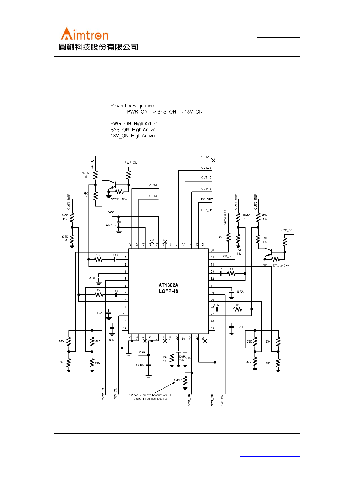
Typical Application
A.
2F, No.10, Prosperity RD. II, Science-Based Industrial Park, Hsinchu 300,Taiwan, R.O.C.
Tel: 886-3-563-0878 WWW: http://www.aimtron.com.tw
Fax: 886-3-563-0879 Email: service@aimtron.com.tw
8
 Loading...