

AIM AT1380A Datasheet
AT1380A
Switching Regulator Controller for LCD Bias
Features
•2.5 to 15 V supply voltage operating range.
•Low current consumption: 6 mA in operation,
1 µA or less in stand-by.
•20 kHz to 1 MHz operation frequency range.
•Provides a fixed output current with minimal
supply voltage fluctuations by using an external
resistor to set the output current.
• Totem-pole output.
• Built-in soft start circuit.
• Built-in timer-latch short circuit detection and
protection circuit (SCP).
Applications
• LCD Displays
• PDAs
• Digital Still Cameras
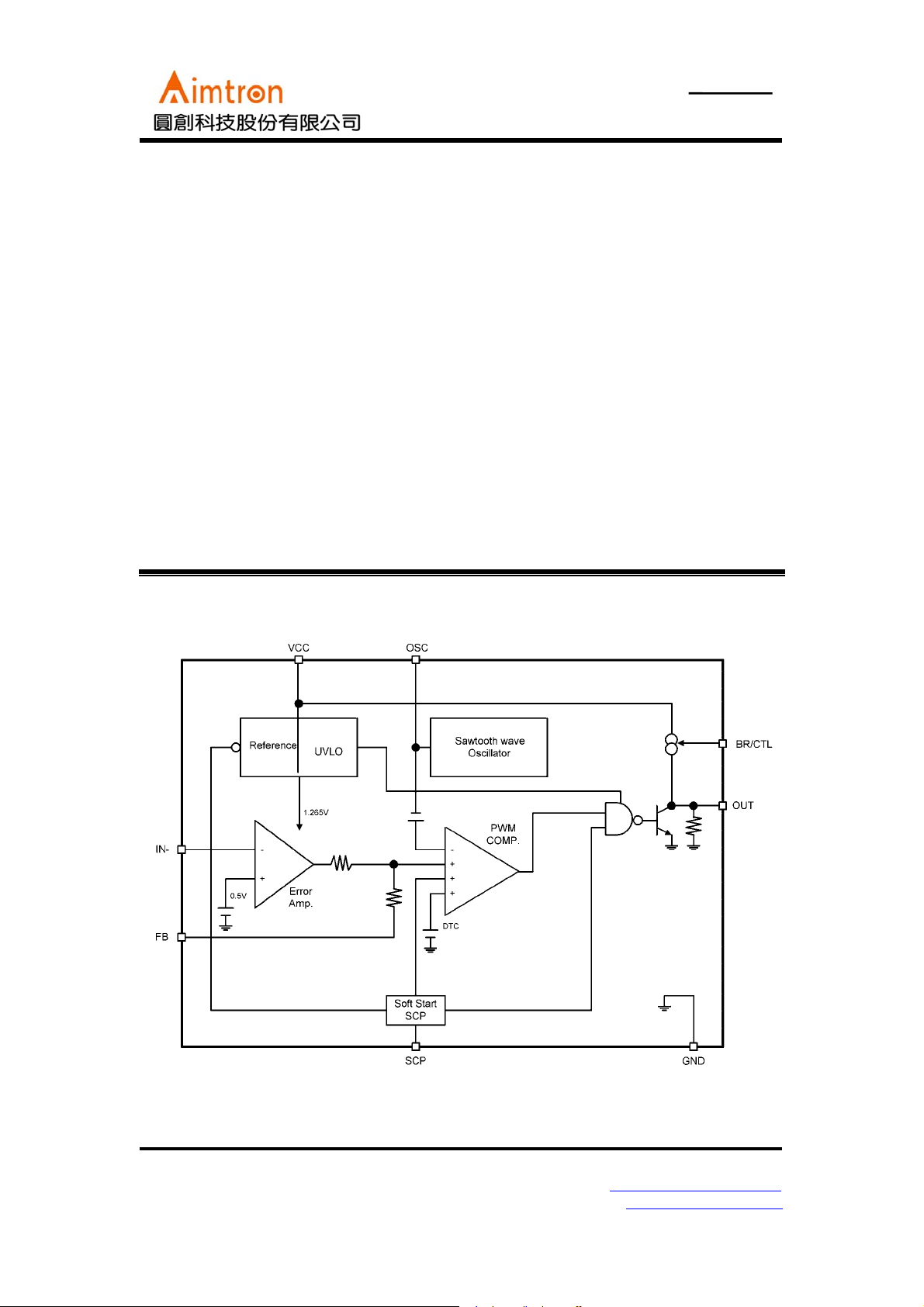
Block Diagram
General Description
The AT1380A is a single-channel PWM control IC
for DC/DC conversion with soft start function and
short circuit detection. Adjustable soft start is
programmed with an external capacitor on SCP
pin. The AT1380A is ideal for up, down and flyback conversion.
2F, No.10, Prosperity RD. II, Science-Based Industrial Park, Hsinchu 300,Taiwan, R.O.C.
Tel: 886-3-563-0878 WWW: http://www.aimtron.com.tw
Fax: 886-3-563-0879 Email: service@aimtron.com.tw
1
AT1380A
Switching Regulator Controller for LCD Bias
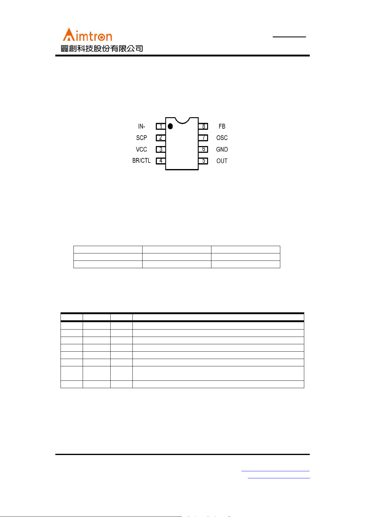
Pin Configuration
Ordering Information
Part number Package Remarks
AT1380A 8-pin Plastic SOP AT1380AS
AT1380A 8-pin TSSOP AT1380AP
Pin Description
Pin No. Symbol I/O Description
1 IN- I Error amplifier inverting input
2 SCP — Soft start and SCP setting capacitor connection
3 VCC — Power supply
4 BR/CTL I Output current setting
5 OUT O Totem-pole type output
6GND—Ground
7 OSC — Capacitor and resistor connection pin for setting the oscillation
frequency
8 FB O Error amplifier output
2F, No.10, Prosperity RD. II, Science-Based Industrial Park, Hsinchu 300,Taiwan, R.O.C.
Tel: 886-3-563-0878 WWW: http://www.aimtron.com.tw
Fax: 886-3-563-0879 Email: service@aimtron.com.tw
2
AT1380A
Switching Regulator Controller for LCD Bias
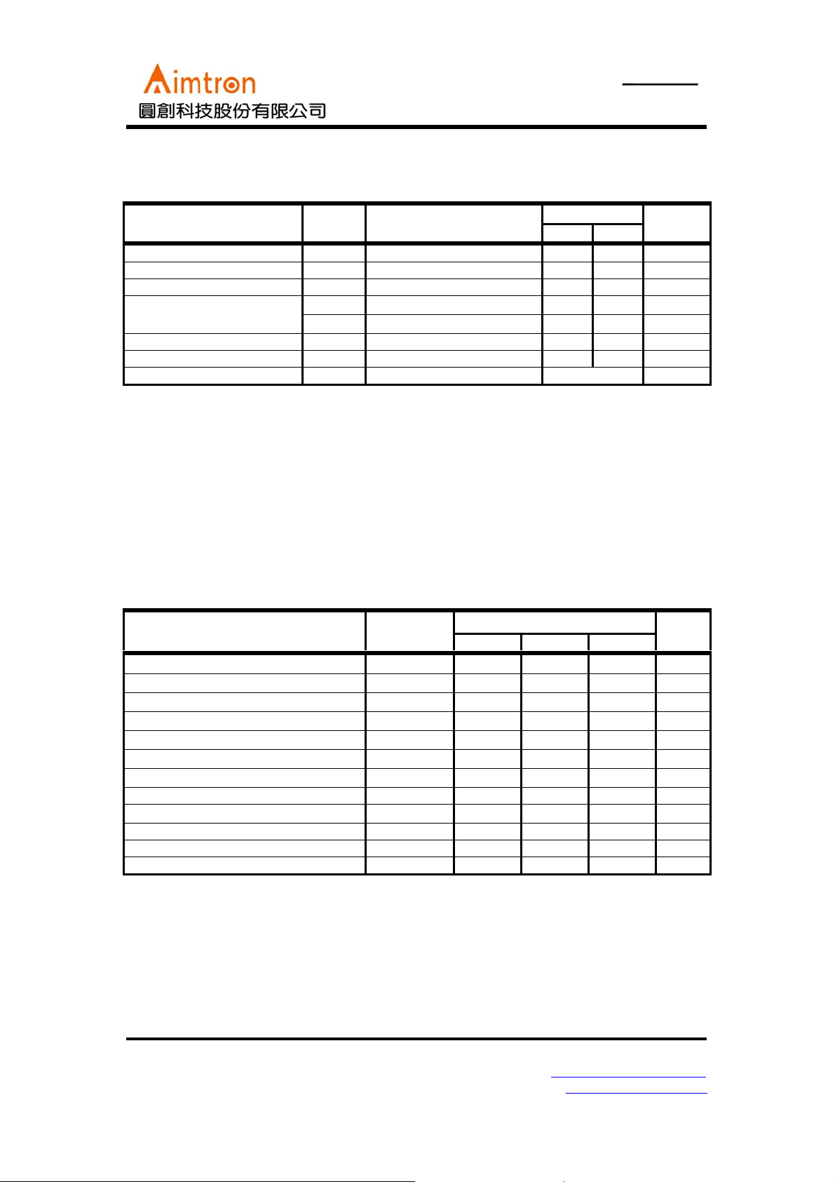
Absolute Maximum Ratings
(Ta=+250C)
Rated ValueParameter Symbol Condition
Unit
Min. Max.
Power supply voltage V
Output source current I
Output sink current I
Allowable dissipation
Operating temperature T
Storage temperature T
CC
+
O
-
O
P
D
P
D
OP
stg
SOP-8, Ta ≦+25°C
TSSOP-8, Ta ≦+25°C
——15V
——-50mA
——50mA
—570 mW
—430 mW
—-30+85
— -55 +125
0
C
0
C
ESD Classification MIL-STD-883 Class 2
* : When mounted on a 10 cm square double-sided epoxy board
WA R N IN G : Do not exceed these ratings. IC devices can be permanently damaged by stress (voltage,
current, temperature, etc.) in excess of absolute maximum ratings.
Recommended Operating Conditions
(Ta=+250C)
Va lu esParameter Symbol
Min. Typ. Max.
Power supply voltage V
Error amplifier input voltage V
BR/CTL pin input voltage V
Output source current I
Output sink current I
SCP pin capacitance C
Phase compensation capacitance C
Output current setting resistance R
Timing resistance R
Timing capacitance C
Oscillation frequency f
Operating temperature T
O
O
OSC
OP
CC
BR
PE
I
+
-
P
B
T
T
2.5 -- 13.5
-0.2 -- 1.0
-0.2 -- V
CC
-20 -- --
-- -- 40
-- 0.1 --
-- 0.1 --
150 390 5000 Ω
1.0 3.0 10.0
100 270 10000 pF
10 500 1000 kHz
-30 +25 +85 °C
WA R N IN G : Recommended operating conditions are normal operating ranges for the IC device. All
the device’s electrical characteristics are warranted for operation within these ranges. Use IC devices
only within the recommended operating conditions. Operation outside these ranges may adversely
affect the reliability and can result in device failure.
Unit
V
V
V
mA
mA
μF
μF
kΩ
2F, No.10, Prosperity RD. II, Science-Based Industrial Park, Hsinchu 300,Taiwan, R.O.C.
Tel: 886-3-563-0878 WWW: http://www.aimtron.com.tw
Fax: 886-3-563-0879 Email: service@aimtron.com.tw
3
AT1380A
Switching Regulator Controller for LCD Bias
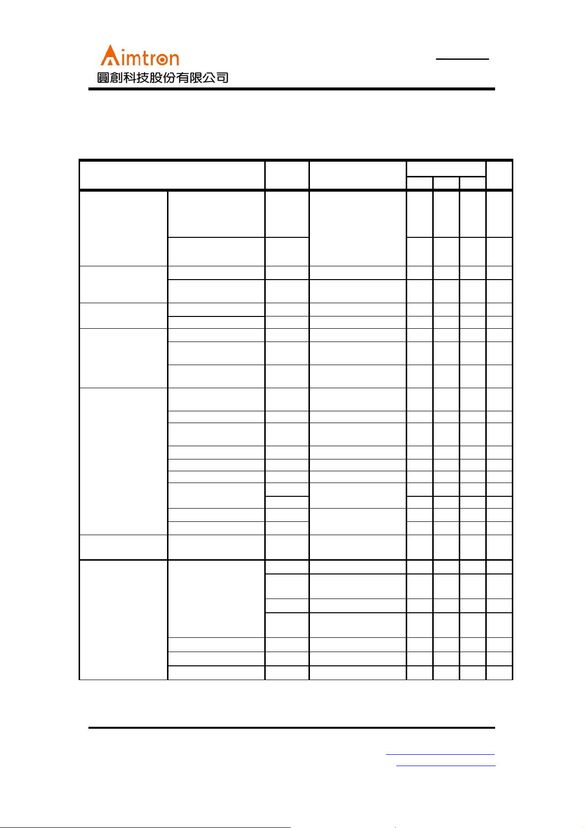
Electrical Characteristics
(VCC=+3.0V, Ta=+250C)
Va lu esParameter Symbol Condition
Min. Typ. Max.
Lockout
(U.V.L.O.)
Reset voltage for
falling Vcc. OUT
remains off if Vcc is
below this level.
Startup voltage for
rising Vcc.
V
R
-- 1.8 1.9 VVCC Under voltage
--
V
TH
2.4 2.5 2.6 V
Unit
Soft start
Short circuit
detection (S.C.P.)
Sawtooth waveform
oscillator (OSC)
Error amplifier
Idle period
adjustment section
Output section
Charging current I
Voltage at soft start
V
CS
V
ts
=0V -1.5 -1.0 -0.7
SCP
-- 0.7 0.8 0.9 V
μA
completion
Charging current I
Threshold voltage V
Oscillation frequency f
Frequency input
V
CPC
OSC
f
tPC
∆V
=0V -1.5 -1.0 -0.7
SCP
-- 0.7 0.8 0.9 V
RT=3kΩ, CT=270pF
400 500 600 kHz
VCC=2.5V to 13.5V -- 2 10 %
μA
Stability
Frequency variation
f
Ta =-300C to 850C--5--%
∆T
with temperature
Input threshold
V
V
T
= 450mV 480 500 520 mV
FB
Voltage
VT input stability V
VT variation with
V
VCC=2V to 13.5V -- 5 20 mV
T∆V
Ta = -300C to 850C--1--%
T∆T
Temperature
Input bias current I
Voltage gain A
Frequency bandwidth BW AV = 0 dB -- 6 -- MHz
V
voltage range
V
Output source current I
Output sink current I
Maximum duty cycle T
V
V
Output voltage
V
V
Output source current I
Output sink current I
Pull down resistance R
VIN = 0V -1.0 -0.2 1.0
B
V
+
OM
_
OM
+
V
OM
OM
DUTY
OH1
OH2
OL1
OL2
O
O
FB
_
RT=3.3kΩ, CT=270pF
f
OSC
RB= 390Ω, IO= -15 mA
RB= 750Ω, VCC = 3.0V
= -10 mA
I
O
RB= 390Ω, IO= -15 mA
RB= 750Ω, VCC = 3.0V
= -10 mA
I
O
+
RB= 390Ω, VO = 0.9V
-
RB= 390Ω, VO = 0.3V
O
-- 70 100 145 V/V
--
0.78 0.87 -- VMaximum output
= 450mV
= 500KHz
-- 20 30 40
μA
-- 0.05 0.2 V
-- -40 -24
24 40 --
μA
μA
75 -- 85 %
1.0 1.2 -- V
0.8 1.0 -- V
-- 0.1 0.2 V
-- 0.1 0.2 V
-- -40 -30 mA
40 70 -- mA
kΩ
2F, No.10, Prosperity RD. II, Science-Based Industrial Park, Hsinchu 300,Taiwan, R.O.C.
Tel: 886-3-563-0878 WWW: http://www.aimtron.com.tw
Fax: 886-3-563-0879 Email: service@aimtron.com.tw
4
 Loading...