

AIC AIC3842CS, AIC3842 Datasheet
PRELIMINARY
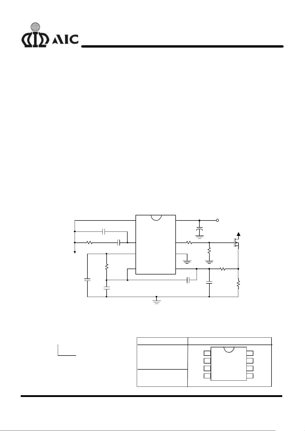
C6
RS
R1
10
R3
51KC50.1µF
+
COMP
VREF
AIC3842
INDUCTOR
SIGNAL
VCC
3
4
VCC
OUTPUT
VFB
PACKAGE TYPE
ORDER NUMBER
PIN CONFIGURATION
AIC3842CX
5 8 7
6
AIC3842
Current-Mode PWM Controller
n FEATURES
l Low Start-Up Current (300 µA Typical)
l Internal Precision Reference.
l 500KHz Current-Mode Operation.
l Pulse-by-Pulse Current Limiting.
l Automatic Feed-Forward Compensation.
l Optimized for Off-Line and DC/DC Converters.
l Undervoltage Lockout with Hysteresis.
l Double Pulse Suppression.
l High Current Totem-Pole Output.
n APPLICATIONS
l Off-Line Converter.
l DC/DC Converter.
n TYPICAL APPLICATION CIRCUIT
2
C2
300pF
FEEDBACK
R4
7.5K
C4
2.2nF
C3
1000P
1
8
RT/CT
n DESCRIPTION
The AIC3842 control IC provides the features
that are necessary to implement off-line or
DC/DC Converter fixed-frequency current-mode
schemes with a minimum number of external
components. This integrated circuits features
an undervoltage lockout (UVLO) with
approximately 300µA start-up current, a
precision reference trimmed for accuracy at the
error amplifier input, high gain error amplifier,
current sensing comparator, logic to insure
latched operation, and a totem-pole output
stage designed to source or sink high peak
current. The output stage, suitable for driving N
channel MOSFETs, is low in the off state.
7
C1
47µF
GND
ISENSE
6
5
300P
R2
20K
R5
390
C7
1nF
M1
0.33
n ORDERING INFORMATION
Analog Integrations Corporation 4F, 9, Industry E. 9th Rd, Science Based Industrial Park, Hsinchu Taiwan, ROC www.analog.com.tw
DS-3842-P1 May 5, 00 TEL: 886-3-5772500 FAX: 886-3-5772510 1
Current Mode PWM Control Circuit
N: PLASTIC DIP
S: SMALL OUTLINE
AIC3842CN
(PLASTIC DIP)
ISENSE
AIC3842CS
(PLASTIC SO)
COMP
VFB
RT/CT
1
2
3
4
VREF
VCC
OUTPUT
GND
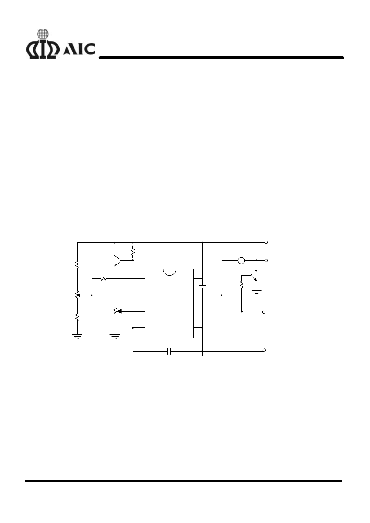
4.7K
4.7K
ISENSE
Q2
2N2222
RT
0.1µF
OUTPUT
CT
GROUND
S1
VCC
V
REF
1W
0.1µF
COMP
VREF
VFB
VCC
RT/CT
OUTPUT
n ABSOLUTE MAXIMUM RATINGS
Supply Voltage (Low Impedance Source ) …..........………….............………........................ 30V
Supply Voltage (ICC<300mA) ...................…..………….… ……..…................……….......... Self Limiting
Output Current ..............………………………....………….................... ……….……….........… ......... ±1A
Output Energy (Capacitive Load) ...................…........…………….….........……….… ...................... 5µJ
Analog Inputs (Pins 2, 3) ….....……………………...…......… ……….................……….... -0.3V to +6.3V
Error Amp Output Sink Current ......…....….……...…………................……….…………............... 10mA
Operation Temperature Range ......…....….……...………….................…………............... -40°C~85°C
Power Dissipation at TA≤25°C DIP Package ......………………………....…………..……............... 1W
SOIC Package .........…….…..….....…………………............. 725mW
Storage Temperature Range .....……...…………...........................… … ......………… -65°C to +150 °C
Lead Temperature (Soldering, 10 seconds) .....……...… ………..…………….……....……........... 300°C
Note 1: All voltages are with respect to Pin 5.
All currents are positive into the specified terminal.
AIC3842
n TEST CIRCUIT
R5
R4
Error Amp.
Adjust
R7
100K
R6
10K
Adjust
R3
5K
ISENSE
AIC3842
GND
C2
A
R1
1K
C1
2
AIC3842
n ELECTRICAL CHARACTERISTICS {V
specified.}
PARAMETERS CONDITIONS MIN. TYP. MAX. UNIT
Reference Section
Output Voltage IO=1mA 4.9 5 5.1 V
Line Regulation
Load Regulation
Temperature Coefficient of
Output Voltage
Output Noise Voltage
Output Voltage Long-Term
Drift
Short-Circuit Output Current
Oscillator Section
Oscillator Frequency (see
Note 3)
Frequency Change with
Supply Voltage
VCC=12V to 25V
IO=1mA to 20mA
f=10Hz to 10KHz
After 1000H at TA=25°C
47 52 57 KHz
VCC=12V to 25V 0.2 %
= 15V (see Note 2), Ta=25°C, unless otherwise
CC
5 20 mV
5 25 mV
0.2 mV/°C
50 µV
5 mV
85 mA
Frequency Change with
Temperature
Peak-to-Peak Amplitude at
RT/CT
Error Amplifier Section
Feedback Input Voltage COMP at 2.5V 2.42 2.50 2.58 V
Input Bias Current
Open-Loop Voltage
Amplification
Gain-Bandwidth Product
Supply Voltage Rejection
Ratio
Output Sink Current VFB at 2.7V, COMP at 1.1V
Output Source Current
High-Level Output Voltage VFB at 2.3V, RL=15KΩ to GND
Low-Level Output Voltage
TA=TLOW to THIGH 5 %
1.7 V
VO=2V to 4V
VCC=12V to 25V
VFB at 2.3V, COMP at 5V
VFB at 2.7V, RL=15Ω to VREF 0.8 V
-0.3 µA
90 dB
1 MHz
70 dB
10 mA
1 mA
6.2 V
3
 Loading...