

AiC AIC3643GG6, AIC3643GK6 Schematic [ru]
Ω
AIC3643
Built-in OVP White LED Step-Up Converter
FEATURES
Built-In Open Circuit Protection
Over Voltage Protection
Efficiency Up to 83% at VIN=4.2V, 3LEDs,
I
=20mA
LED
1.2MHz Fixed Switching Frequency
Drives Up to 5LEDs in series
2.5V to 5.5V Input Voltage
Low Supply Current: 150μA
Matches LED Current
Requires Tiny Inductor and Capacitors
TSOT-23-6, and SOT-23-6 Packages
DESCRIPTION
AIC3643 is a current-mode pulse-widthmodulation (PWM), step-up DC/DC converter
designed to drive white LEDs with a constant
current to provide backlight in hand-held devices.
Series connection of LEDs provides identical
LED currents resulting in uniform brightness.
This configuration eliminates the need of ballast
resistors. The built-in open load protection
prevents the damage resulting from an open
circuit condition. Also low 100mV feedback
voltage minimizes power loss in the current
setting resistor for better efficiency.
APPLICATIONS
Cellular Phones
PDAs
DSCs
Handheld Devices
White LED Display Backlighting
AIC3643 is a step-up PWM converter, which
includes an internal N-channel MOSFET switch
for high efficiency. The high switching frequency,
1.2MHz, allows the use of tiny external
components.
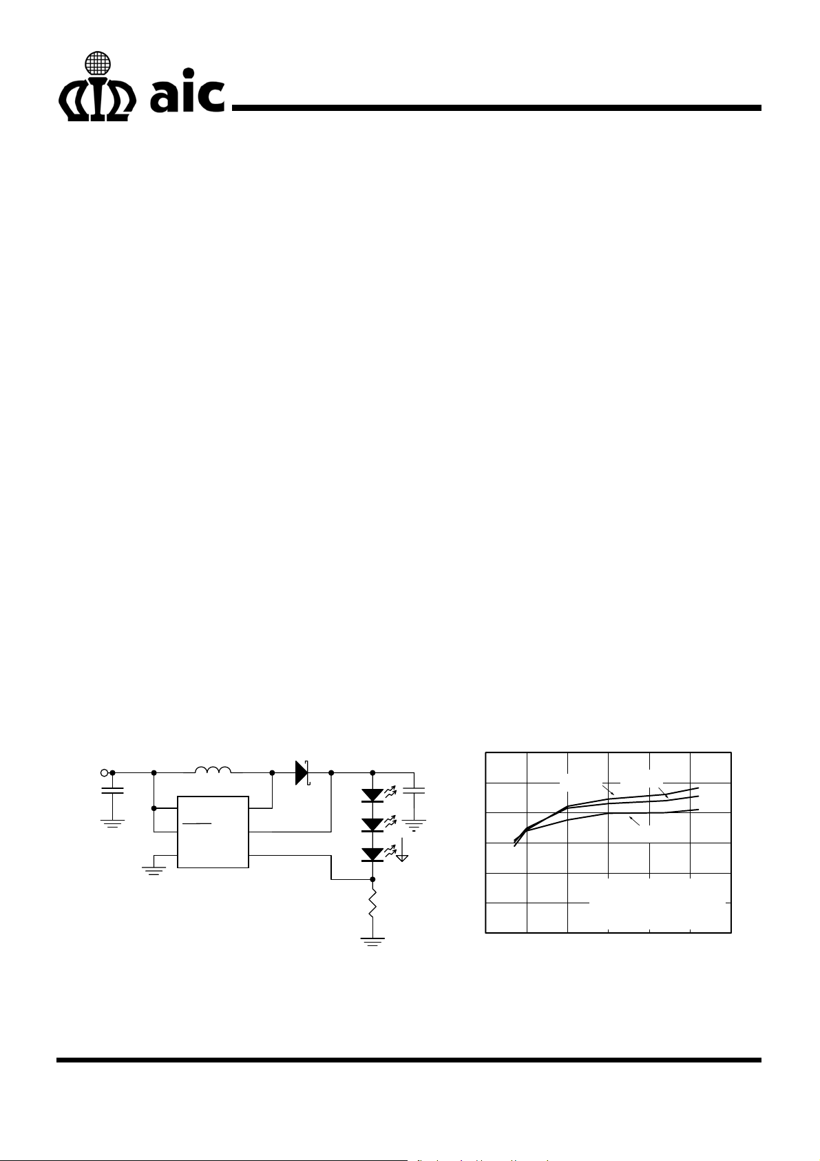
TYPICAL APPLICATION CIRCUIT
3.0~4.2V
C1
1μF
L1: GTSD31-6R8M, GOTREND
D1: SS0540, PAN JIT
C1: JMK107BJ105KA, TAIYO YUDEN
C2: GRM21BR61C335K, MURATA
L
6.8μH
VIN
SHDN
GND
AIC3643
SW
OVP
FB
Fig. 1 Li-Ion Powered Driver for Three White LEDs
D1
RFB
5
C2
3.3μF
20mA
AIC3643 is available in a space-saving TSOT23-6, and SOT-23-6 packages.
90
85
80
75
70
Efficiency (%)
65
60
0 5 10 15 20 25 30
VIN=4.2V
LED Current (mA)
VIN=3.6V
VIN=3V
3 LEDs, 6.8μH
L1: GTSD31-6R8M, GOTREND
D1: SS0540, PAN JIT
Test Circuit refer to Fig.1
Analog Integrations Corporation Si-Soft Research Center DS-3643G-01 20090820
3A1, No.1, Li-Hsin Rd. I, Science Park, Hsinchu 300, Taiwan, R.O.C.
TEL: 886-3-5772500 FAX: 886-3-5772510 www.analog.com.tw
1
A
AIC3643
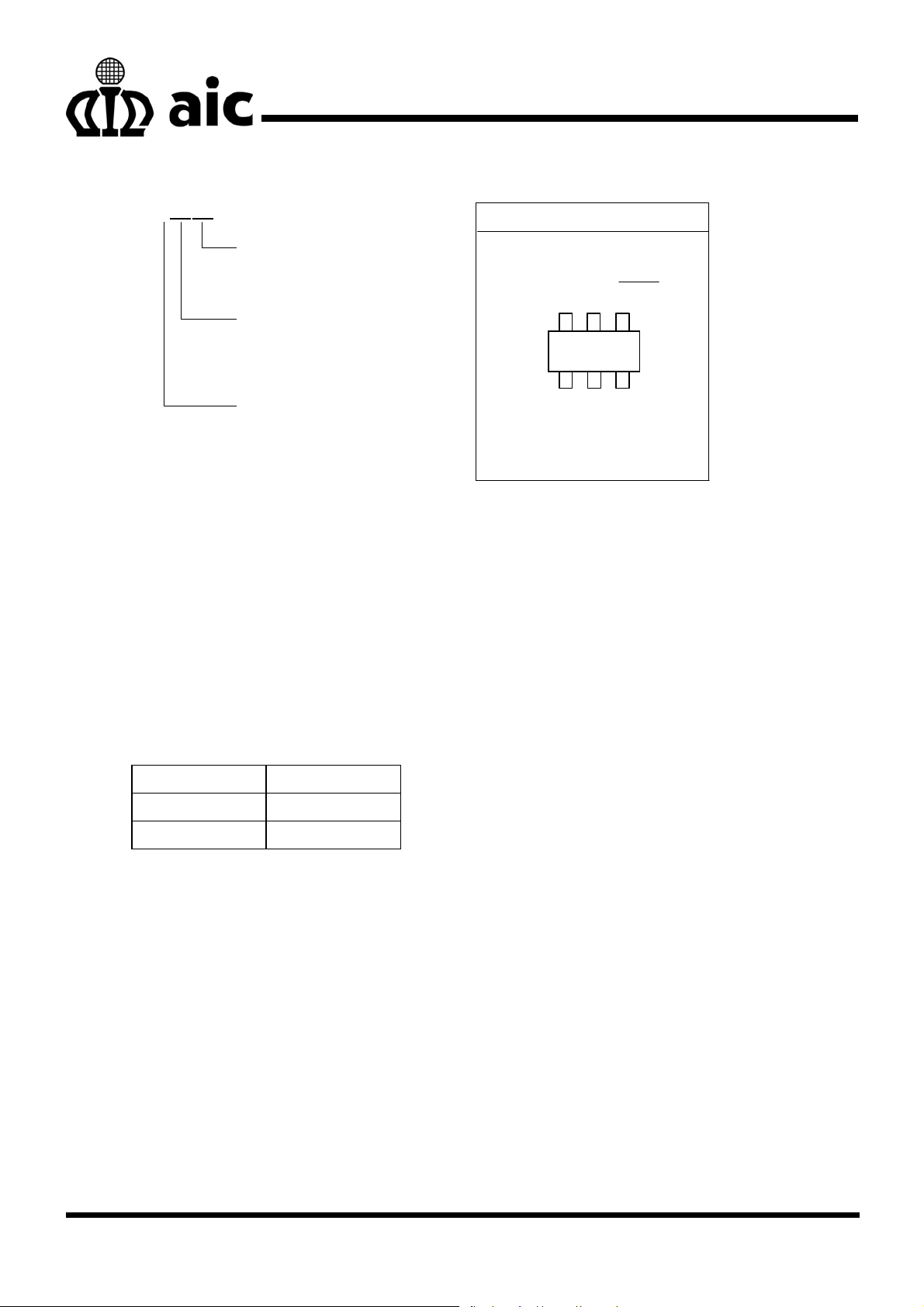
ORDERING INFORMATION
IC3643XXX XX
PIN CONFIGURATION
PACKING TYPE
TR: TAPE & REEL
BG: BAG
PACKAGE TYPE
G6: SOT-23-6
K6: TSOT-23-6
G: Green Package
Example: AIC3643GG6TR
in SOT-23-6 Green Package &
Tape & Reel Packing Type
SOT-23-6
TSOT-23-6
FRONT VIEW
OVP
5
2
GNDSW
SHDN
4
3
FB
VIN
6
3643G/3643K
1
Note: Pin1 is determined by orienting
the package marking as shown.
Marking
Part No. Marking
AIC3643GG6 3643G
AIC3643GK6 3643K
2
AIC3643
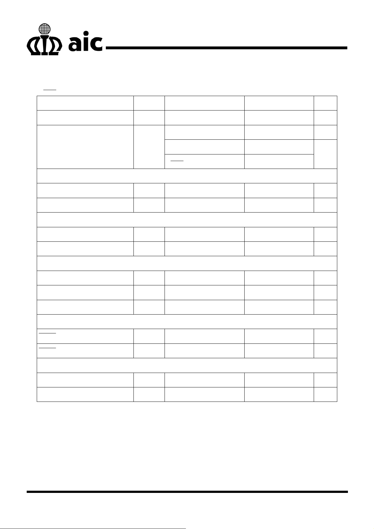
ABSOLUTE MAXIMUM RATINGS
Input Voltage (VIN) 6V
SW Voltage
FB Voltage
SHDN
OVP Voltage
Operating Temperature Range
Storage Temperature Range
Maximum Junction Temperature
Lead Temperature (Soldering, 10 sec)
Thermal Resistance Junction to Case SOT-23-6
TSOT-23-6
Thermal Resistance Junction to Ambient SOT-23-6
TSOT-23-6
Absolute Maximum Ratings are those values beyond which the life of a device may be impaired.
Voltage 6V
–40°C to 85°C
–65°C to 150°C
33V
6V
34V
150°C
260°C
115°C/W
115°C/W
250°C/W
250°C/W
3
AIC3643
ELECTRICAL CHARACTERISTICS
(V
=1.5V, VIN=3V, TA=25°C, unless otherwise specified.) (Note 1)
SHDN
PARAMETER SYMBOL TEST CONDITIONS MIN TYP MAX UNIT
Operating Voltage VIN 2.5 5.5 V
Switching 1 3 mA
Supply Current IIN
Non switching 150 270
V
= 0V 0.1 1.0
SHDN
ERROR AMPLIFIER
V
Feedback Voltage
FB Input Bias Current
90 100 110 mV
FB
I
FB
V
FB
=100mV
1 nA
OSCILLATOR
Switching Frequency f
0.8 1.2 1.6 MHz
OSC
Maximum Duty Cycle D 91 94 %
μA
POWER SWITCH
SW ON Resistance R
Switch Leakage Current I
DS(ON)
SW(OFF)VSW
1.4 2.5 Ω
=33V 0.1 1 μA
Switch Current Limit IIL 0.65 1 A
CONTROL INPUT
SHDN Voltage High V
SHDN
Voltage Low V
ON 1.5 V
IH
OFF 0.3 V
IL
OVER VOLTAGE PROTECTION
OVP Input Resistance R
OVP Threshold V
0.8 1.2 1.6 MΩ
OVP
1V Hysteresis typical 22 28 32 V
OVP
Note 1: Specifications are production tested at TA=25°C. Specifications over the -40°C to 85°C operating
temperature range are assured by design, characterization and correlation with Statistical Quality
Controls (SQC).
4
AIC3643
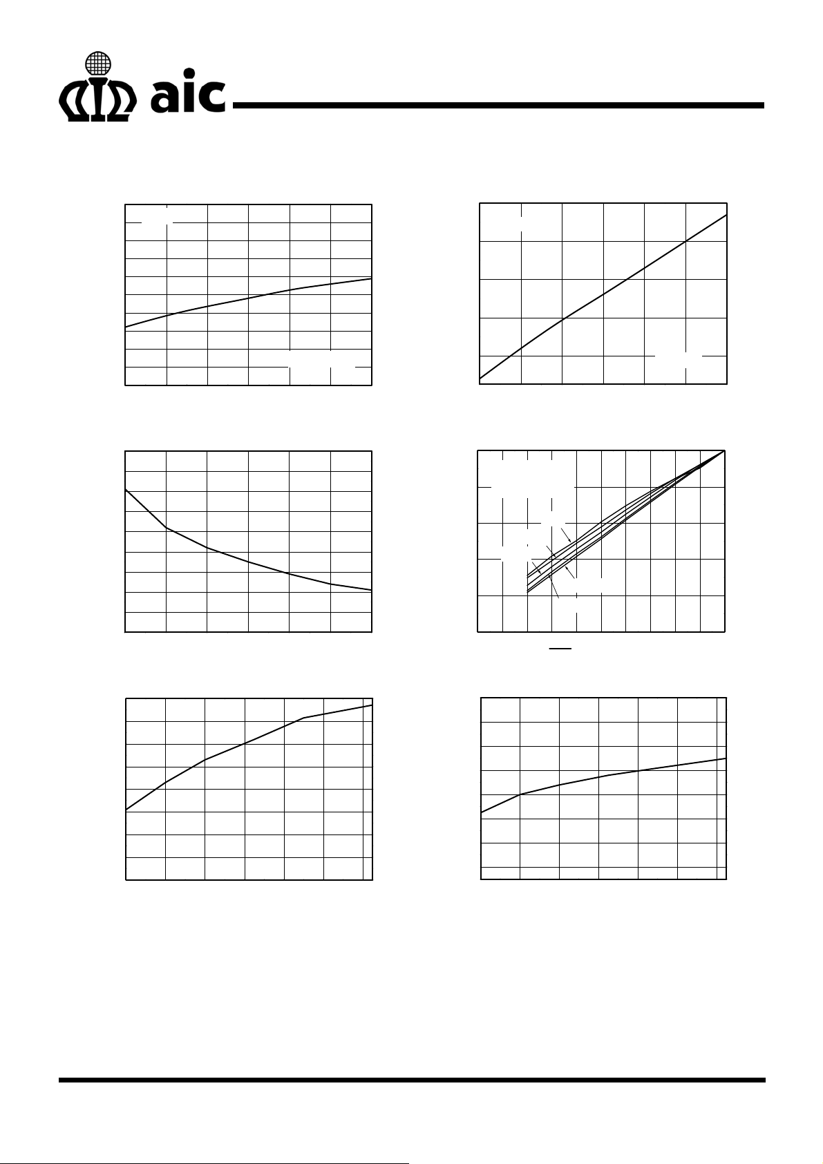
TYPICAL PERFORMANCE CHARACTERISTICS
200
FB=V
190
180
170
160
150
140
130
Supply Current (μA)
120
110
100
2.5 3.0 3.5 4.0 4.5 5.0 5.5
Fig. 2 Supply Current vs. Supply Voltage Fig. 3 Supply Current vs. Supply Voltage
IN
Non-Switching
Supply Voltage (V)
1600
FB=GND
1400
1200
1000
Supply Current (μA)
800
2.5 3.0 3.5 4.0 4.5 5.0 5.5
Supply Voltage (V)
Switching
1.7
1.6
1.5
1.4
1.3
(Ω)
1.2
DS-ON
R
1.1
1.0
0.9
0.8
2.53.03.54.04.55.05.5
Fig. 4 R
1.6
1.5
1.4
1.3
1.2
1.1
1.0
Switching Frequency (MHz)
0.9
0.8
-40-200 20406080
100
VIN=3.6V; L=6.8μH
C
=1μF; C
500Hz
=3.3μF
OUT
2kHz
1kHz
100Hz
200Hz
SHDN PIN PWM Duty (%)
Temperature (oC)
IN
80
3LEDs
60
(%)
LEDMAX
/I
40
LED_DUTY
I
20
0
0 102030405060708090100
Supply Voltage (V)
vs. Supply Voltage Fig. 5 Dimming Control by Shutdown Pin
DS_ON
Temperature (oC)
110
108
106
104
102
100
98
Feedback Voltage (mV)
96
-40-200 20406080
Fig. 6 Switching Frequency vs. Temperature Fig. 7 Feedback Voltage vs. Temperature
5
 Loading...