

AIC AIC1811CCV, AIC1811BCV, AIC1811 Datasheet
AIC1811
µ
µ
M1
BATTERY
One-Cell Lithium-Ion Battery Protection IC
n FEATURES
l Reduction in Board Size due to Miniature
Package SOT-23-5 and Less External
Components.
l Ultra-Low Quiescent Current at 7
l Ultra-Low Power-Down Current at 0.4
=2.3V).
l Precision Overcharge Protection Voltage
4.35V ± 50mV for the AIC1811A
4.30V ± 50mV for the AIC1811B
4.25V ± 50mV for the AIC1811C
l Built-in Delay Time Circuits for Overcharge,
Over-discharge, and Overcurrent Protection.
l Load Detection Function during Overcharge
Mode.
l Two Detection Levels for Overcurrent Protection.
A (VCC=3.5V).
A (V
CC
n DESCRIPTION
The AIC1811 battery protection IC is designed to
protect lithium-ion battery from damage or
degrading the lifetime due to overcharge,
overdischarge, and/or overcurrent for one-cell
lithium-ion battery powered systems, such as
cellular phones. The ultra-small package and less
required external components make it ideal to
integrate the AIC1811 into the limited space of
battery pack.
The accurate ±50mV overcharging detection
voltage ensures safe and full utilization charging.
Three different specification values for overcharge
protection voltage are provided for various
protection requirements. The very low standby
current drains little current from the cell while in
storage.
n APPLICATIONS
l Protection IC for One-Cell Lithium-Ion Battery
Pack.
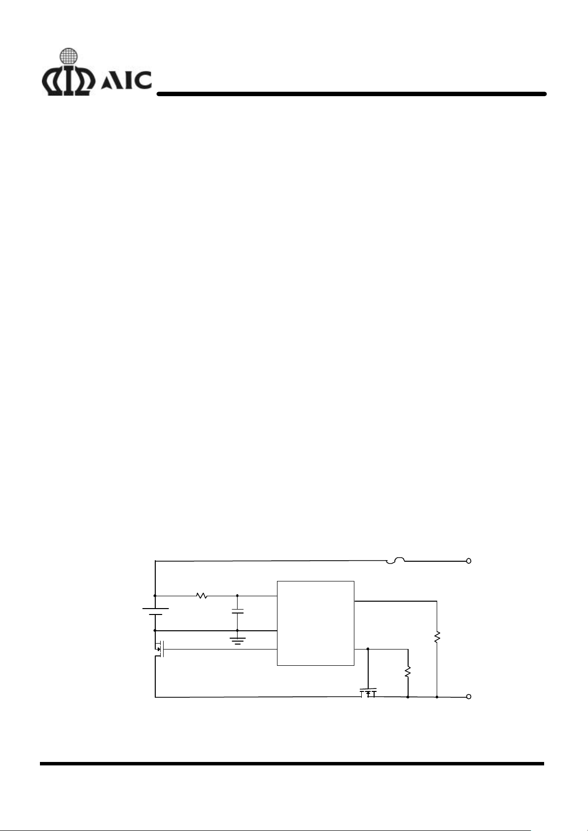
n TYPICAL APPLICATION CIRCUIT
R1
100
SI9926
Protection Circuit for One -Cell Lithium-Ion Battery
C1
0.1µF
5
VCC
2
GND
3
OD
AIC1811
CS
OC
4
1
M2 SI9926
BATT+
FUSE
R2
51K
R3
10M
BATT-
DS-1811-00 June 7, 00 www.analog.com.tw
1
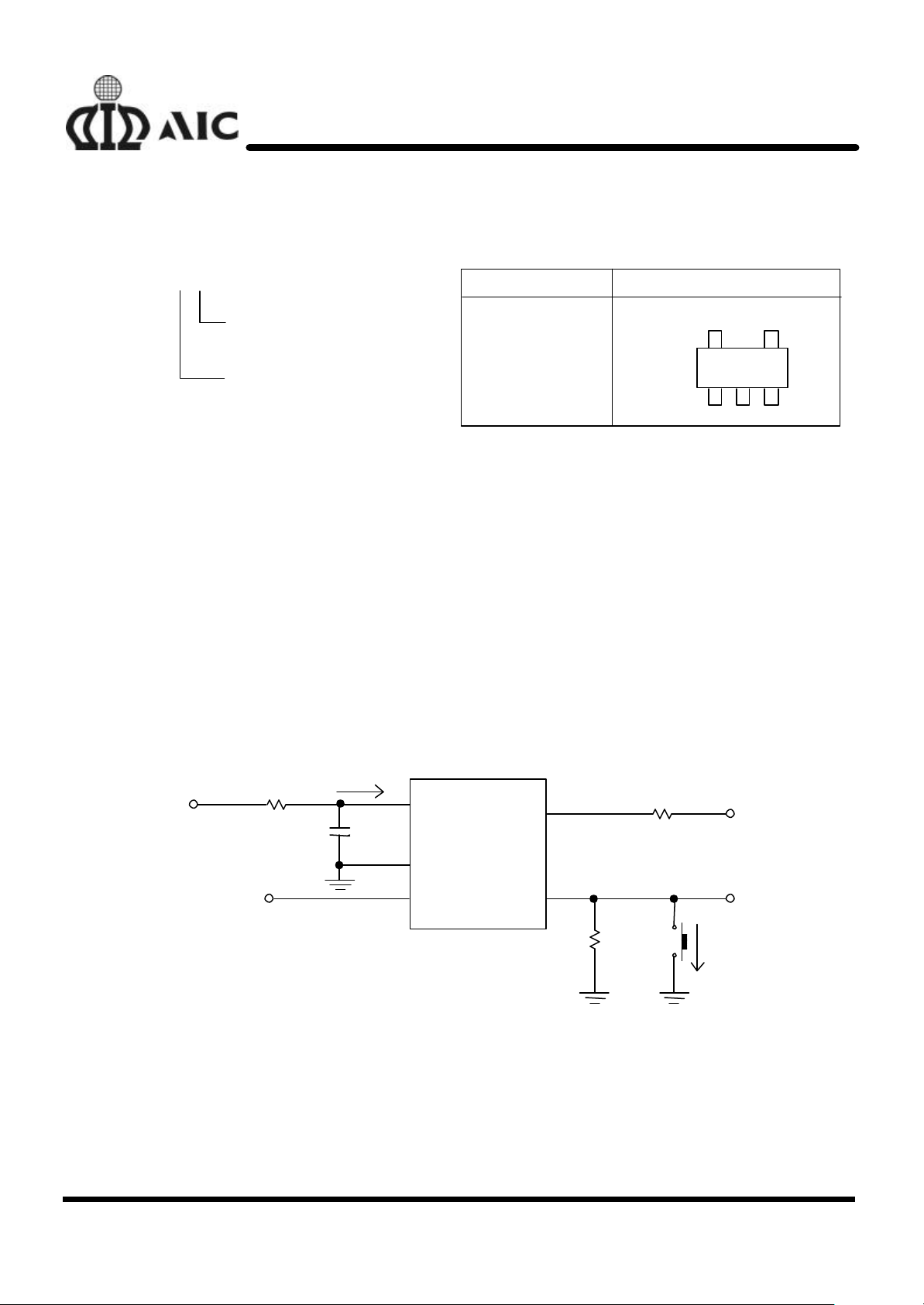
n ORDERING INFORMATION
V: SOT-2
OD
OC
AIC18
11
XC
X
4
5
AIC1811
ORDER NUMBER PIN CONFIGURATION
PACKAGE TYPE
3-5
AIC1811ACV
AIC1811BCV
TOP VIEW
AIC1811CCV
OVERCHARGE PROTECTION
(SOT-23-5)
A: 4.35V
B: 4.30V
C: 4.25V
n ABSOLUTE MAXIMUM RATINGS
Supply Voltage ....................................……………..................................................... 18V
DC Voltage Applied on other Pins ...............………………………….............................. 18V
Operating Temperature Range .....................................……………….............. -40°C~85°C
Storage Temperature Range .........................…………………..................... - 65°C~125°C
n TEST CIRCUIT
VCC
CS
321
GND
I
V
CC
R1
100
V
OD
CC
C1
0.1µF
5
VCC
2
GND
3
OD
AIC1811
CS
OC
4
1
R3
10M
R2
51K
S1
V
CS
V
OC
I
OC
2
AIC1811
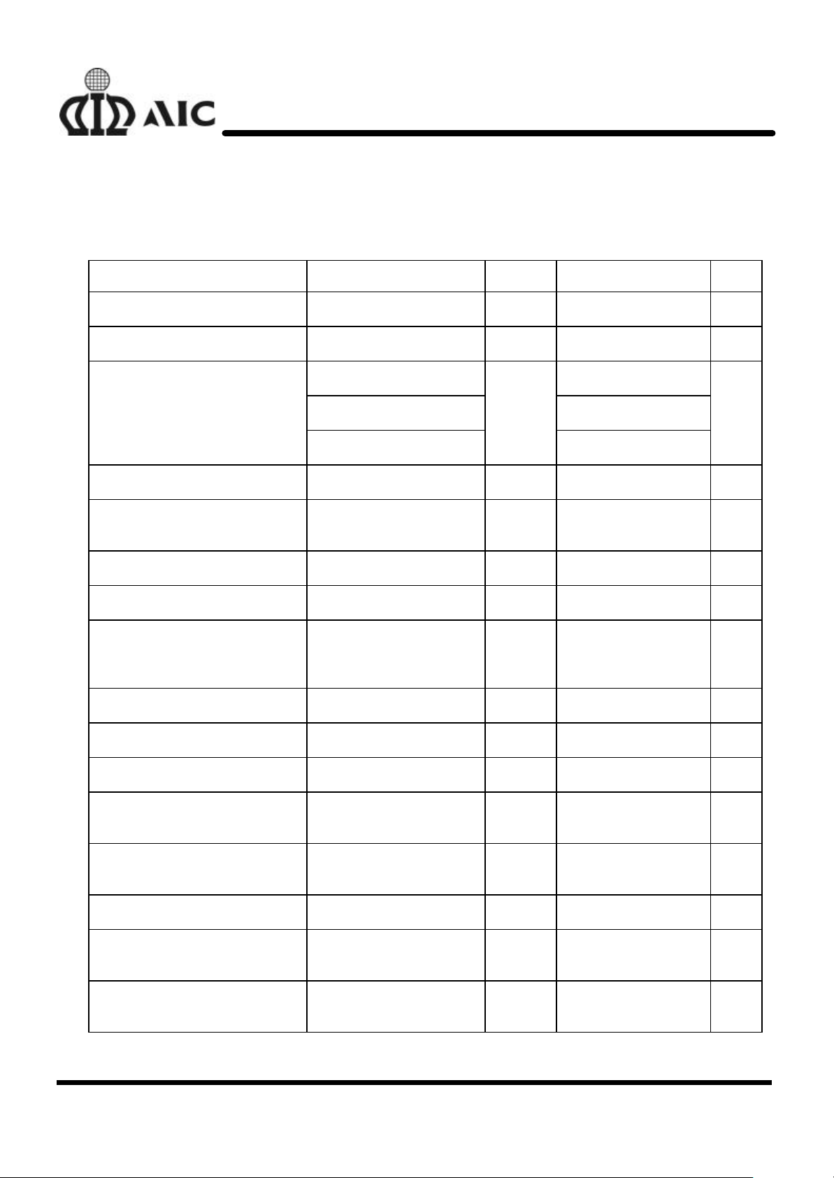
n ELECTRICAL CHARACTERISTICS (Ta=25 °C, unless otherwise specified.)
PARAMETER TEST CONDITIONS
SYMBOL
Supply Current VCC=3.5V I
Power-Down Current VCC=2.3V, I
Overcharge Protection Voltage
AIC1811A 4.30 4.35 4.40
AIC1811B 4.25 4.30 4.35
V
AIC1811C
Overcharge Hysteresis Voltage V
Overdischarge Protection
V
Voltage
Overdischarge Release Voltage V
Overcurrent Protection Voltage VCC=3.5V V
Overcharge Delay Time VCC=V
V
OCP
-0.1→
OCP
+ 0.1V
CC
PD
OCP
HYS
ODP
ODR
T
OIP
OC
MIN. TYP. MAX. UNIT
7 11 µA
0.4 1.0 µA
V
4.20 4.25 4.30
150 200 250 mV
2.2 2.4 2.6 V
2.6 2.9 3.2 V
180 200 220 mV
50 100 150 mS
Overdischarge Delay Time VCC= 2.5V →2.3V T
Overcurrent Delay Time (1) VCC=3.5V, 1V>VCS>0.2V T
Overcurrent Delay Time (2) VCC=3.5V, VCS>1V T
OC Pin Source Current VCC=3.5V, OC pin short to
GND
OD Pin Output “H” Voltage
V
OD Pin Output “L” Voltage V
Load Dectection Threshold
Voltage
Charge Detection Threshold
Voltage
VCC=V
–50mV V
OCP
VCC=2.3V V
I
OD
OI1
OI2
OC
DH
DL
LD
CH
50 100 150 mS
5 10 15 mS
150 300 450 µS
240 340 440 µA
VCC-0.1
VCC-
0.02
V
0.01 0.1 V
0.3 0.4 V
-0.45 -0.3 V
3
 Loading...