

AIC AIC1802CCS, AIC1802BCS, AIC1802 Datasheet

AIC1802
µ
µ
*C
TC
*C
TD
1µF
M2
Q1
Two-Cell Lithium-Ion Battery Protection IC
n FEATURES
l Ultra-Low Quiescent Current at 10
VC=3.5V).
l Ultra-Low Power-Down Current at 0.2
=3.8V, VC=1.9V).
l Wide Supply Range: 2 to 18V.
l Precision Overcharge Protection Voltage
4.35V ± 30mV for the AIC1802A
4.30V ± 30mV for the AIC1802B
4.25V ± 30mV for the AIC1802C
l Built-in Delay Circuits for Overcharge, Over-
discharge and Overcurrent Protection.
l Overcharge and Overdischarge Delay Time
can be Extended by External Capacitors.
l Built-in Cell-balancing Bleeding Network under
Overcharge Condition.
n APPLICATIONS
l Protection IC for Two-Cell Lithium-Ion Battery
Pack.
A (VCC=7V,
A (V
CC
n DESCRIPTION
The AIC1802 battery protection IC is designed
to protect lithium-ion batteries from damage due
to overcharging, overdischarging, and
overcurrent for two series cells in portable
phones and laptop computers. It can be a part of
the low-cost charge control system within a twocell lithium-ion battery pack.
Safe and full utilization charging is ensured by
the accurate ±30mV overcharge detection.
Three different specification values for
overcharge protection voltage are provided for
various protection requirements. The very low
standby current drains little current from the
cells while in storage.
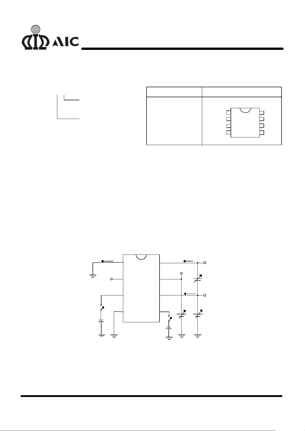
n TYPICAL APPLICATION CIRCUIT
**R1
C1
C2
BATTERY 2
M1
CEM9926
1µF
**R2
*CTC & CTD are optional for delay time adjustment.
**R1 & R2: Refer application informations.
Protection Circuit for Two-Cell Lithium-Ion Battery Pack
DS-1802-03 July 13, 00 www.analog.com.tw
8
VCC TC
6
VC TD
4
GND OC
2
OD CS
AIC1802
5
3
1
7
R6
1K
R3
1M
CEM9926
C3
0.01µF
V
+
BAT
R4
1M
R5
1M
V
-
BAT
1
n ORDERING INFORMATION
AIC1
802ACS
VCVCODTD
GNDCSTC
OC13428657
+
+
V
V
432
1
I
V
CSCTC
V
COICC
AIC1802
AIC1802 XCX
PACKAGE TYPE
S: SOP-8
OVERCHARGE
PROTECTION VOLTAGE
A: 4.35V
B: 4.30V
C: 4.25V
ORDER NUMBER
AIC1802BCS
AIC1802CCS
(PLASTIC SO8)
PIN CONFIGURATION
TOP VIEW
n ABSOLUTE MAXIMUM RATINGS
Supply Voltage ....................................……………..................................................... 18V
DC Voltage Applied on VC, CS, OC, OD Pins ...............…………….............................. 18V
DC Voltage Applied on TC, TD Pins ...............…………………..…….............................. 5V
Operating Temperature Range .......................................….………….............. -40°C~85°C
Storage Temperature Range .........................…………………..................... - 65°C~150°C
n TEST CIRCUIT
I
OC VCC
OD CS
TD VC
GND TC
C
TD
AIC1802
8
7
6
5
CC
2
AIC1802
n ELECTRICAL CHARACTERISTICS (Ta=25 °C, unless otherwise specified.)
PARAMETER TEST CONDITIONS SYMBOL MIN. TYP. MAX. UNIT
Supply Current in Normal Mode VCC=7V, VC=3.5V I
Supply Current in Power-Down
Mode
VCC=4.8V, VC=2.4V I
VC Pin Input Current VCC=7V, VC=3.5V I
AIC1802A 4.32 4.35 4.38
AIC1802B 4.27 4.30 4.33 Overcharge Protection Voltage
V
AIC1802C
Overcharge Release Voltage V
Overdischarge Protection
Voltage
V
Overdischarge Release Voltage V
Overcurrent Protection Voltage VCC=7V V
Overcharge Delay Time (1)
VCC=8.6V, VC=4.3V,
CTC=0µF
T
CC
PD
C
OCP
OCR
ODP
ODR
OIP
OC1
10 15 µA
0.8 1.2 µA
400 600 nA
V
4.22 4.25 4.28
3.85 4.0 4.15 V
2.25 2.4 2.55 V
2.85 3.0 3.15 V
135 150 165 mV
12 25 38 mS
Overcharge Delay Time (2)
Overdischarge Delay Time (1)
Overdischarge Delay Time (2)
Overcurrent Delay Time (1)
Overcurrent Delay Time (2)
OC Pin Source Current
VCC=8.6V, VC=4.3V,
CTC=0.47µF
VCC=4.8V, VC=2.4V,
CTD=0µF
VCC=4.8V, VC=2.4V,
CTD=0.47µF
VCC=7V, VC=3.5V,
VCS=0.15V
VCC=7V, VC=3.5V,
VCS=0.36V
VCC=8.6V, VC=4.3V,
OC Pin Short to GND
T
T
T
OD Pin Output “H” Voltage V
T
T
I
OC2
OD1
OD2
OI1
OI2
CO
DL
0.7 1.1 1.5 S
12 25 38 mS
0.7 1.1 1.5 S
4 9 14 mS
1.0 2.0 3.0 mS
270 400 530 µA
VCC-0.1 VCC-0.02 V
3
 Loading...