

AIC AIC1781CS, AIC1781 Datasheet
AIC1781
/
/
g
(
)
/
/
/
Battery Charge Controller
FEATURES
Fast Charge Control of NiMH/NiCd Batteries,
even with a Fluctuating Charging Current.
∆∆T
Fast Charge Termination by:
0V∆
, Safety Timer, Maximum Temperature,
t, −∆V
Maximum Voltage.
∆∆T
Linearly Adjustable
t
Detection Slope and
Safety Timer.
Adjustable Peak Voltage Timer for
Battery Voltage Protection Range Selectable.
Selectable Battery Temperature Protection
0V∆
.
Mode.
Protection against Battery Voltage and Battery
Temperature Faults.
Selectable LED Display Mode for Battery Status.
Five Pulsed Trickle Charge Modes.
Discharge-before-Charge Function Available for
Eliminating Memory Effect.
Quick and Easy Testing for Production.
16-pin DIP or SO Packages.
APPLICATIONS
Battery Fast Chargers for:
Mobile Phones.
Notebook and Laptop Personal Computers.
Portable Power Tools and Toys.
Portable Communication Equipments.
Portable Video & Stereo Equipments.
1.55
Charge Current = 600 mA
Cell Capacit y = 550 mA
NiMH Battery
1.45
V
e
1.35
Cell Volta
1.25
1.15
Cell Voltage
Temperature
0 102030405060
Charge Time (min.)
100
80
60
40
Temperature (°C)
20
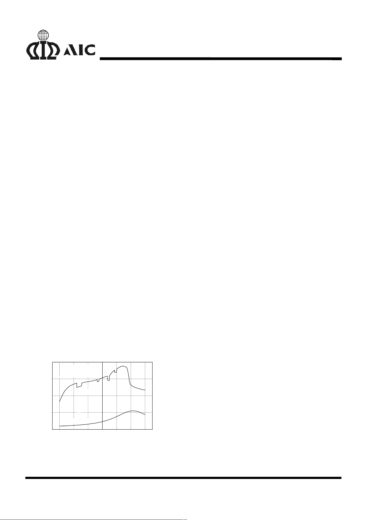
Fig. 1 Battery Charging Characteristics Resulting
from an AIC1781-Controlled Charger with a
Fluctuating Charging Current
DESCRIPTION
The AIC1781 fast charge controller IC is designed
for intelligent charging of NiMH or NiCd batteries
,
without the risk of overcharge.
∆∆T
0V∆
detection (peak voltage timer)
t
detection are the primary methods
(-0.25%),
and
−∆V
detection
employed by the AIC1781 to terminate fast charge.
The fast charge can also be cut off by maximum
battery voltage and maximum battery temperature
detection along with the safety timer to prevent
charging under fault conditions of the charging
system or the battery itself.
∆∆T
Both
t
and
−∆V
detection methods have
been proved powerful in terminating fast charging
for NiMH and NiCd batteries. The AIC1781 utilizes
the combination of these two methods to achieve
reliable decision of ending fast charge and prevent
misaction caused by using
−∆V
detection alone
under certain conditions. Fig. 1 shows an example
of charging curve of a battery charged by a
fluctuating current from a NiMH battery charger
which uses the AIC1781 controller IC to achieve
optimal charging. This technique, in cooperating
with the
0V∆
detection (peak voltage timer), is
particularly suitable for NiMH batteries, whose
voltage drop is hardly significant yet temperature
rises rapidly. The
t
or
−∆V
detection
∆∆T
circuitry may be disabled independently for
different applications, such as system-integrated
chargers, chargers with varying charge current, or
battery packs lack of temperature sensing
thermistor.
The safety timer period, mode of battery
temperature protection, battery voltage protection
range, pulsed trickle charge duty, and LED display
mode are all adjustable or selectable. Dischargebefore-charge function is included to get rid of
memory effect of NiCd batteries without the risk of
overdischarging. Test mode is provided for charger
manufactures to dramatically reduce production
test time.
Analog Integrations Corporation 4F, 9, Industry E. 9th Rd, Science Based Industrial Park, Hsinchu Taiwan, ROC www.analog.com.tw
DS-1781-00 TEL: 886-3-5772500 FAX: 886-3-5772510
1
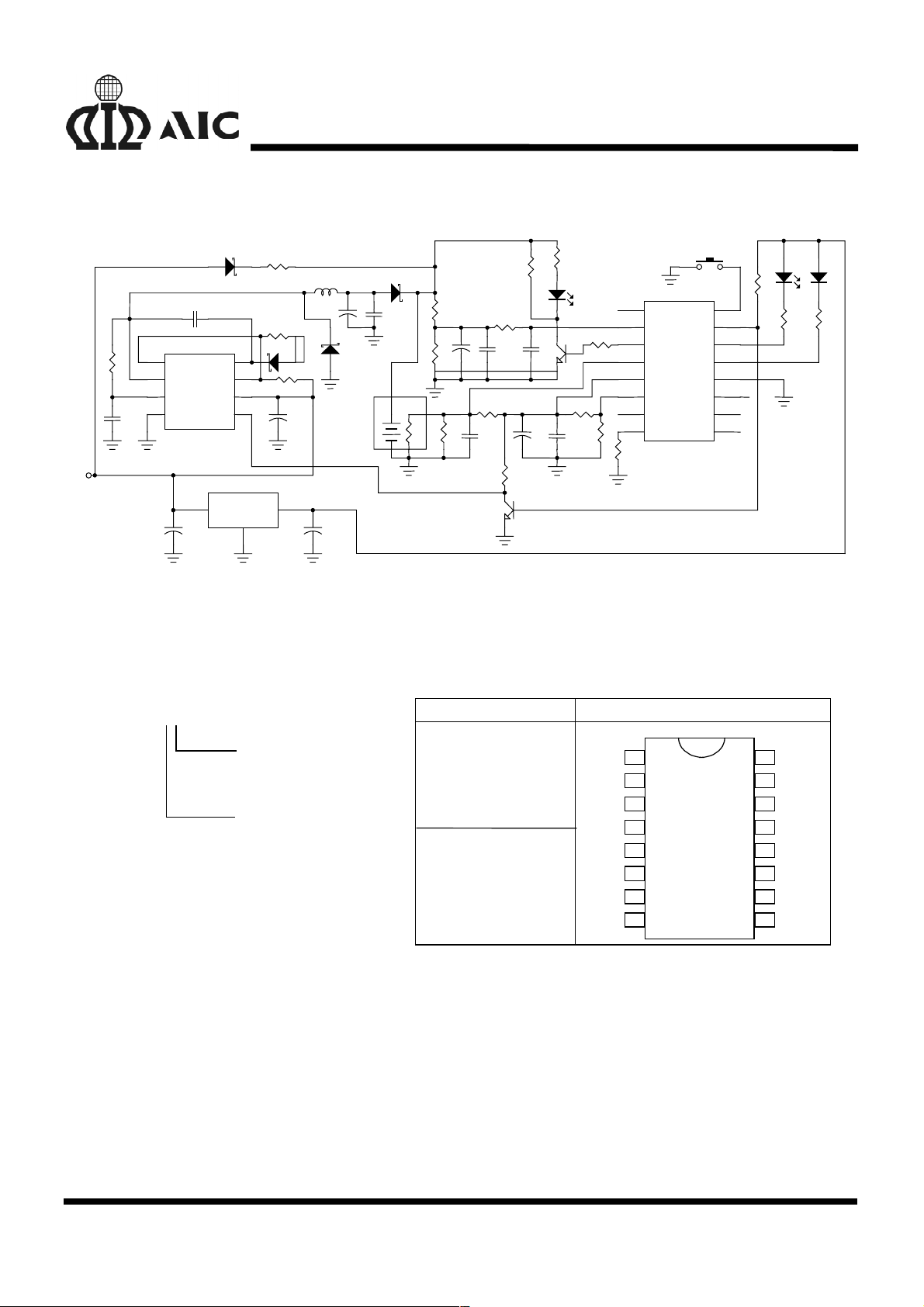
TYPICAL APPLICATION CIRCUIT
µ
A
A
A
(
)
A
AIC1781
VIN
R4
390K
C1
1000P
D1
IN4148
C2
1µF
U1
1
DC
DE
CF
GND
+
C12
1uF
AIC1563
1
BOOST
IS
VCC
FB
U3 7805
VIN
2
3
4
2
8
7
6
5
VOUT
GND
R1
1K
R5 120/0.5W
D3
IN4148
R6
0.3/1W
+
C3
220µF
3
L1
220µH
+
C13
10µF
Battery Charge Circuit for Fluctuating Charging Current Application
ORDERING INFORMATION
IC1781XX
+
C4
220µF
D4
1N5819
BAT1
BATTERY
D2 IN4148
C5
.1µF
0
R9
240K
R8
120K
R7
THERMIS TOR
ORDER NUMBER
RY1
100K
+
C9
4.7µF
2N3904
RX1
100K
C6
0.1
470K
Q2
SW PB
AIC1781
DSW
ICON
LED2
LED1
GND
SEL1
SEL2
MODE
SW1
LED3
LED2
R12
GREEN
100K
16
15
14
13
12
11
10
9
R16
680
RED
R17
680
R3
R2
C10
47nF
+
C11
100µF
270
Q1
2N3904
C8
0.1µF
LED1
YELLOW
R15
680
R14
200K
R18
50K
R11
100K
1
PEAK
2
VBT
3
DIS
4
VTS
5
VCC
6
ADJ
7
SEL3
8
TMR
20/5W
R10
100K
C7
0.1µF
F
R13
PIN CONFIGURATION
PACKAGE TYPE
N: PLASTIC DIP
S: SMALL OUTLINE
IC1781CN
(PLASTIC DIP)
PEAK
VBT
DIS
TEMPERATURE RANGE
C= 0°C~70°C
IC1781CS
PLASTIC SO
VTS
VCC
DJ
SEL3
TMR
ABSOLUTE MAXIMUM RATINGS
Supply Voltage ............................................…………........................................ 5.5V
DC Voltage Applied on any pin ......................……………...................................... 5.5V
Sink current of ICON pin, LED1 and LED2 pin .......................……….................. 20mA
Operating Temperature Range .....................................…………….............. 0°C~ 70°C
Storage Temperature Range .............................................…………...... -65°C~ 150°C
1
2
3
4
5
6
7
8
16
15
14
13
12
11
10
9
DSW
ICON
LED2
LED1
GND
SEL1
SEL2
MODE
2
TEST CIRCUIT
A
V
CC
VOLTAGE
SOURCE
-+
YELLOW
R1
560
-+
VOLTAGE SOURCE
VCC (5V)
V
V1 (0.95V)
CC
PEAK DSW
VBT ICON
DIS LED2
VTS LED1
AIC1781
VCC GND
DJ SEL1
R3
560
R4
560
R5
560
ORANGE
GREEN
RED
V
CC
AIC1781
V
CC
V2 (3V)
100K
ELECTRICAL CHARACTERISTICS (Ta=25°
SEL3 SEL2
TMR MODE
R2
PARAMETER TEST CONDITIONS SYMBOL MIN. TYP. MAX. UNIT
Supply Voltage V
Supply Current I
Voltage Protection Limit
Battery Low
During Initial Timer 0.11 0.16 0.21
After Initial Timer
(SEL3>3V) 0.63 0.69 0.75
(SEL3<2V) 1.1 1.2 1.30
Battery High
(SEL3>3V) 2.6 2.7 2.80
(SEL3<2V)
V
CC
V
CC
°C, VCC=5V, unless otherwise specified.)
°°
CC
CC
V
BT
4.5 5.0 5.5 V
1.1 mA
V
1.9 2.0 2.10
3
AIC1781
ELECTRICAL CHARACTERISTICS (Ta=25°
PARAMETER TEST CONDITIONS SYMBOL MIN. TYP. MAX. UNIT
Temperature High 1.35 1.45 1.55
Temperature Sense Limit
Temperature Low
Output impedance of DIS Pin Z
LED1, LED2, ICON Pins
Output Impedance
ON
OFF 1
Source Current
Capability
SEL3 pin
DSW pin
MODE, PEAK, SEL1,
Input Impedance
SEL2 pins 300 KΩ
VBT, VTS, ADJ pins 1 MΩ
Recommended
External Resistor of TMR pin
°C, VCC=5V, unless otherwise specified.)
°°
V
TS
DIS
3.5 3.6 3.70
140 250 Ω
25 50 Ω
I
SEL3
I
DSW
R
TMR
2 100 1000 KΩ
5.5
16
V
MΩ
µA
-∆V Detection Level w.r.t.*
Peak Value
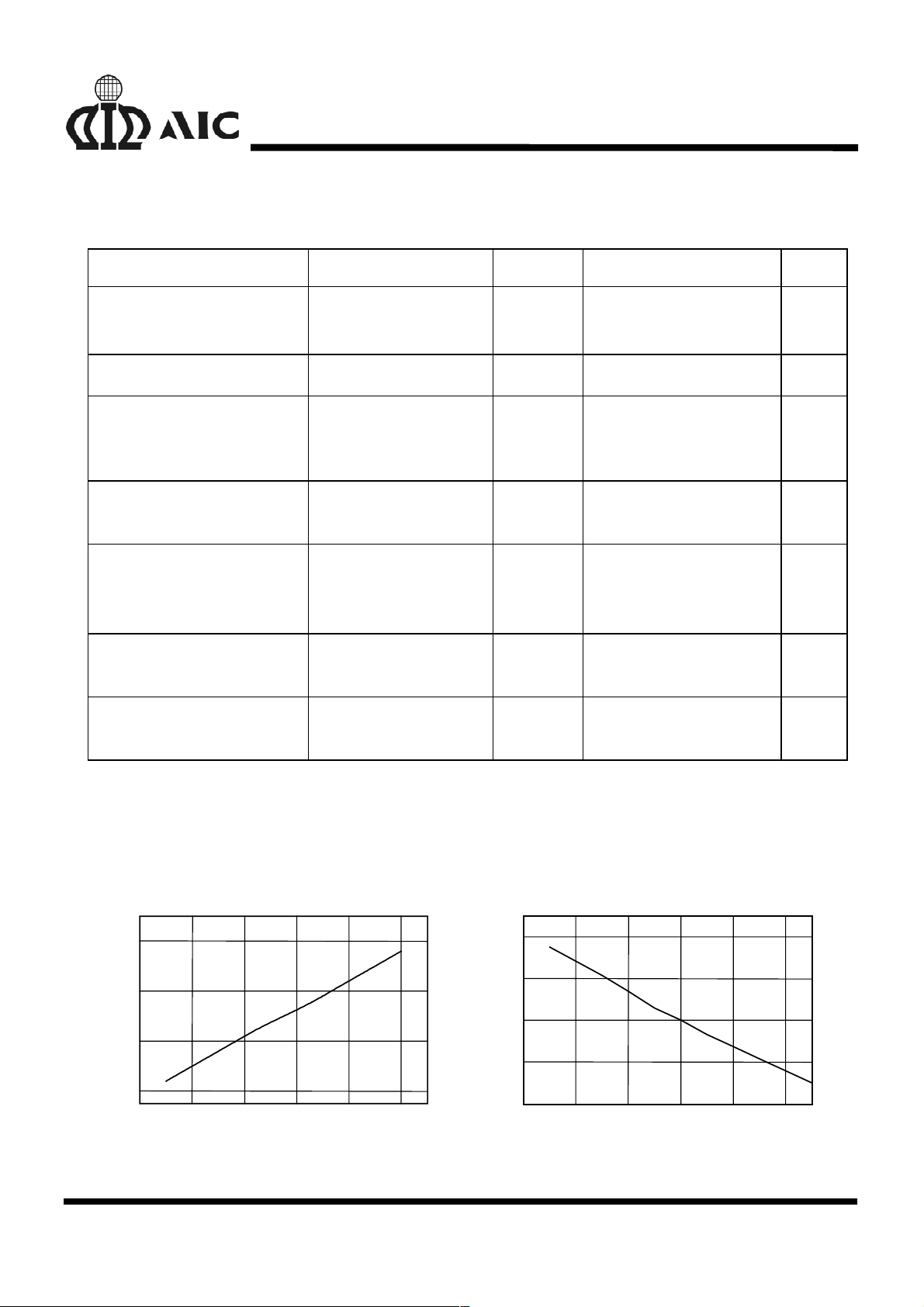
TYPICAL PERFORMANCE CHARACTERISTICS (Ta=25°
V
=5V, refer to Test Circuit)
CC
1.21
1.18
1.12
1.06
Supply Current (mA)
1.00
4.4 4.6 4.8 5.0 5.2 5.4
Supply Current vs Supply Voltage
VCC (V)
81.0
80.5
80.0
Safety Timer (min.)
79.5
79.0
4.4 4. 6 4.8 5. 0 5.2 5.4
Safety Timer vs Supply Volatge
-0.25 %
°C, R2=100KΩΩΩΩ,
°°
VCC (V)
4
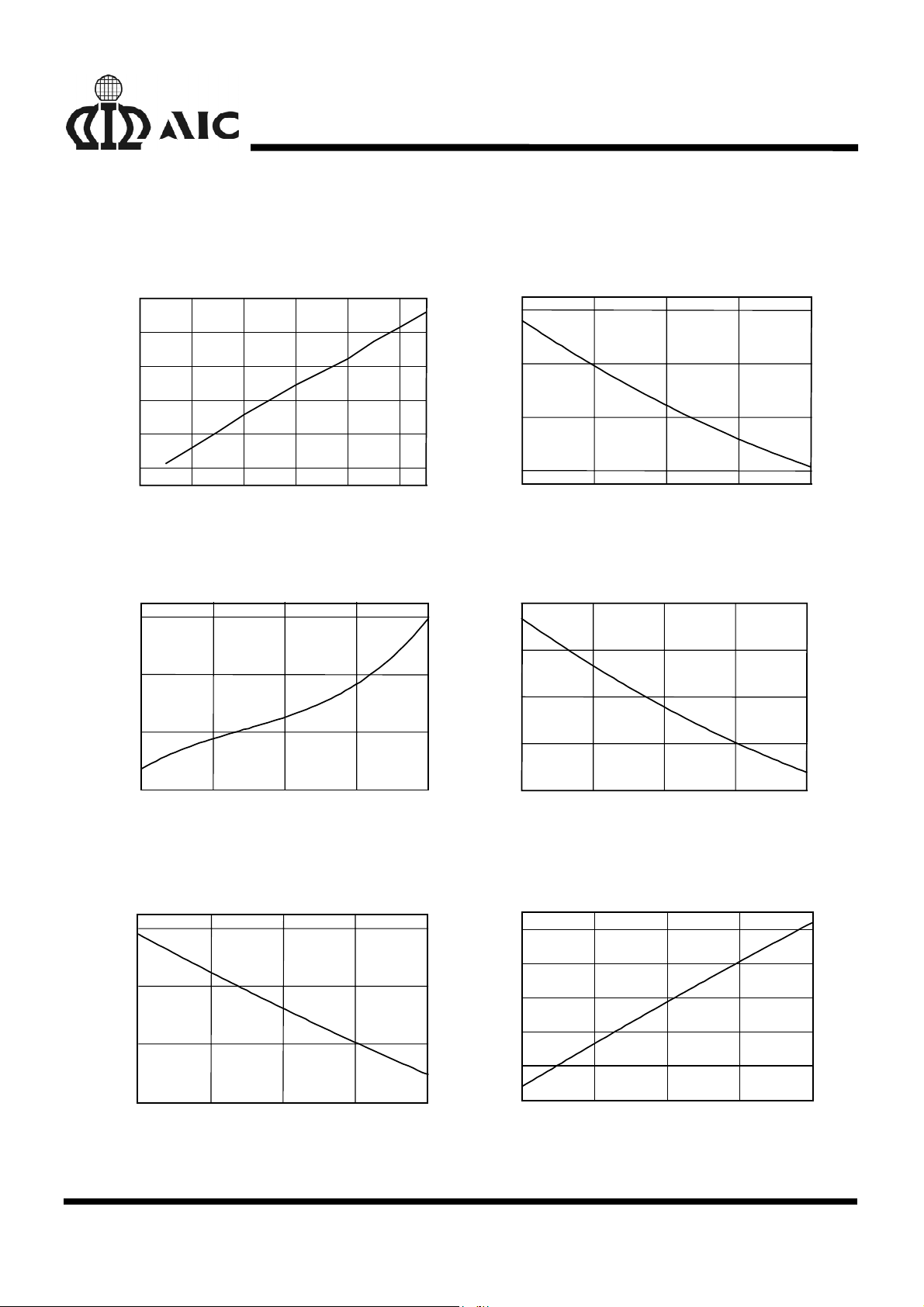
TYPICAL PERFORMANCE CHARACTERISTICS (Continued)
AIC1781
LED Flashing Frequency vs Supply Voltage
4.8
4.6
4.4
4.2
Frequency (Hz)
4.0
3.8
4.44.64.85.05.25.4
V
CC
(V)
Safety Timer vs Temperature
82.0
81.0
80.0
Safety Timer (min.)
Supply Current vs Temperature
1.26
1.14
1.02
Supply Curr ent (mA)
0.9
020406080
Temperature (°C)
LED Flashing Frequency vs Temperature
5.0
4.6
4.2
Fre quenc y ( Hz)
3.8
79.0
0
20 40 60 80
Temperature(°C)
VBT (high) Limit vs Temperature
(SEL3>3V)
2.74
2.70
(V)
BT
V
2.66
2.62
0 20406080
Temperature (°C)
3.4
020406080
Temperature(°C)
VBT (high) Limit vs Temperature
(SEL3<2V)
2.03
2.01
(V)
BT
V
1.99
1.98
0
20 40 60 80
Temperature (°C)
5
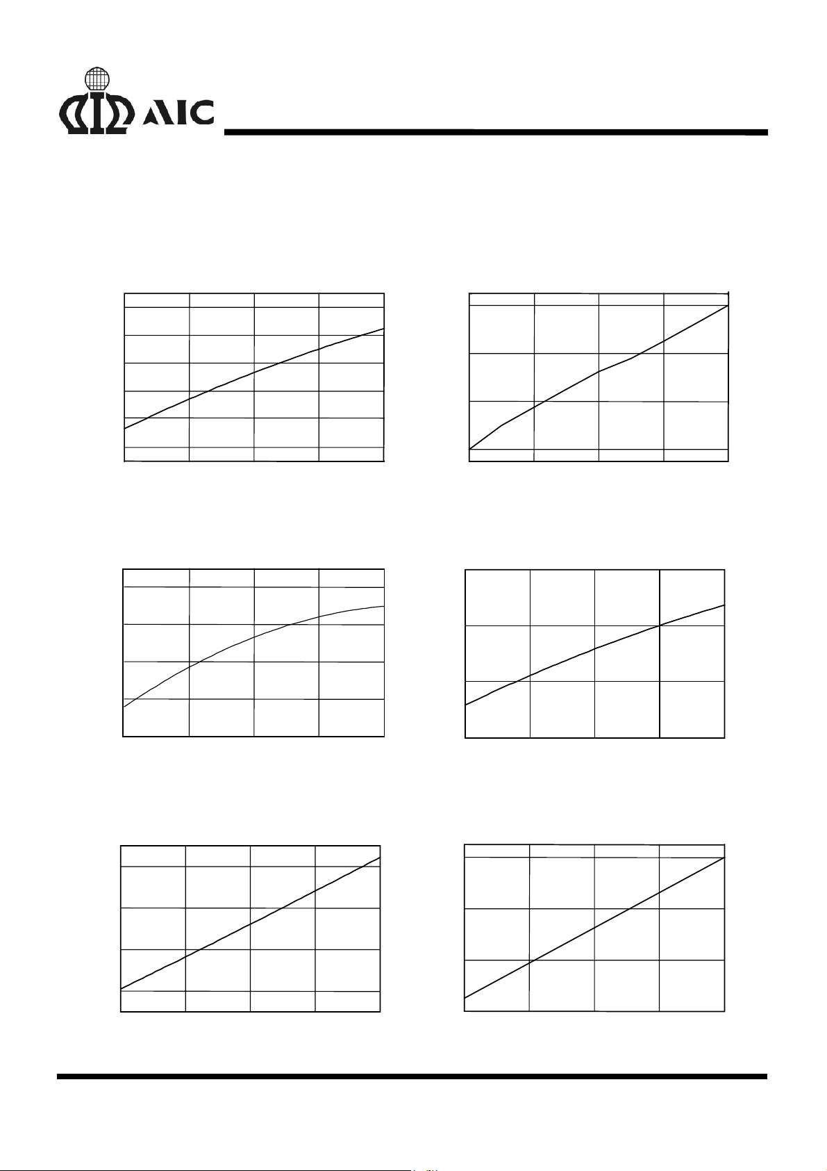
TYPICAL PERFORMANCE CHARACTERISTICS (Continued)
(
)
AIC1781
VBT (low) Limit vs Temperature (During Initial Timer)
0.163
0.162
0.161
(V)
BT
V
0.160
0.159
0.158
0 20406080
Temperature (°C)
VTS (high) Limit vs Temperature
3.62
3.61
(V)
TS
3.60
V
3.59
Output Impedance vs Temperature
(LED1,LED2,ICON pins)
29
)
Ω
27
25
Output Impedance(
23
020406080
Temperature (°C)
VTS (low) Limit vs Temperature
1.48
1.46
(V)
TS
V
1.44
3.58
0 20406080
Temperature (°C)
V
Limits vs Temperature
BT(LOW)
(SEL3>3V, After Initial Timer)
0.700
0.695
(V)
BT
V
0.690
0.685
020
40
Temperature (°C)
60 80
1.42
1.24
1.22
0
20 40 60 80
Temperature (°C)
Limits vs Temperature
V
BT(LOW)
(SEL3<3V, After Initial Timer)
V
BT
V
1.20
1.18
0 20406080
Temperature (°C)
6
 Loading...