

AIC AIC1740-30CY, AIC1740-30CF, AIC1740-30CE, AIC1740-27CY, AIC1740-27CF Datasheet
...
µ
µ
AIC1740
AIC1740
Low Output Voltage, 500mA Low Dropout
Linear Regulator
n FEATURES
l Low Dropout Voltage of 900mV at 500mA
Output Current (3.0V Output Version).
l Guaranteed 500mA Output Current.
l Internal 1.5Ω P-MOSFET Draws no Base
Current.
l Low Ground Current at 65
l 2% Accuracy Output Voltage of 1.8V/ 2.0V/
A.
2.5V/ 2.7V/ 3.0V.
l Input Voltage Range up to 12V.
l Needs only 4.7
l Current and Thermal Limiting.
F for Stability.
n APPLICATIONS
l Voltage Regulator for CD-ROM Drivers.
l Voltage Regulator for LAN Cards.
l Voltage Regulator for Monitor Microprocessor.
l Voltage Regulator for RAM Module.
l Wireless Communication Systems.
l Battery Powered Systems.
n DESCRIPTION
The AIC1740 is a 3-pin low dropout linear
regulator. The superior characteristics of the
AIC1740 include zero base current loss, very
low dropout voltage, and 2% accuracy output
voltage. Typical ground current remains
approximately
65µA, from no load to maximum loading
conditions. Dropout voltage is exceptionally low.
Output current limiting and thermal limiting are
built in to provide maximal protection to the
AIC1740 against fault conditions.
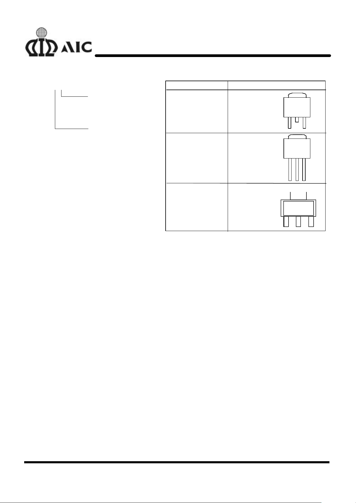
The AIC1740 comes in the popular SOT-223,
TO-251 and TO-252 packages.
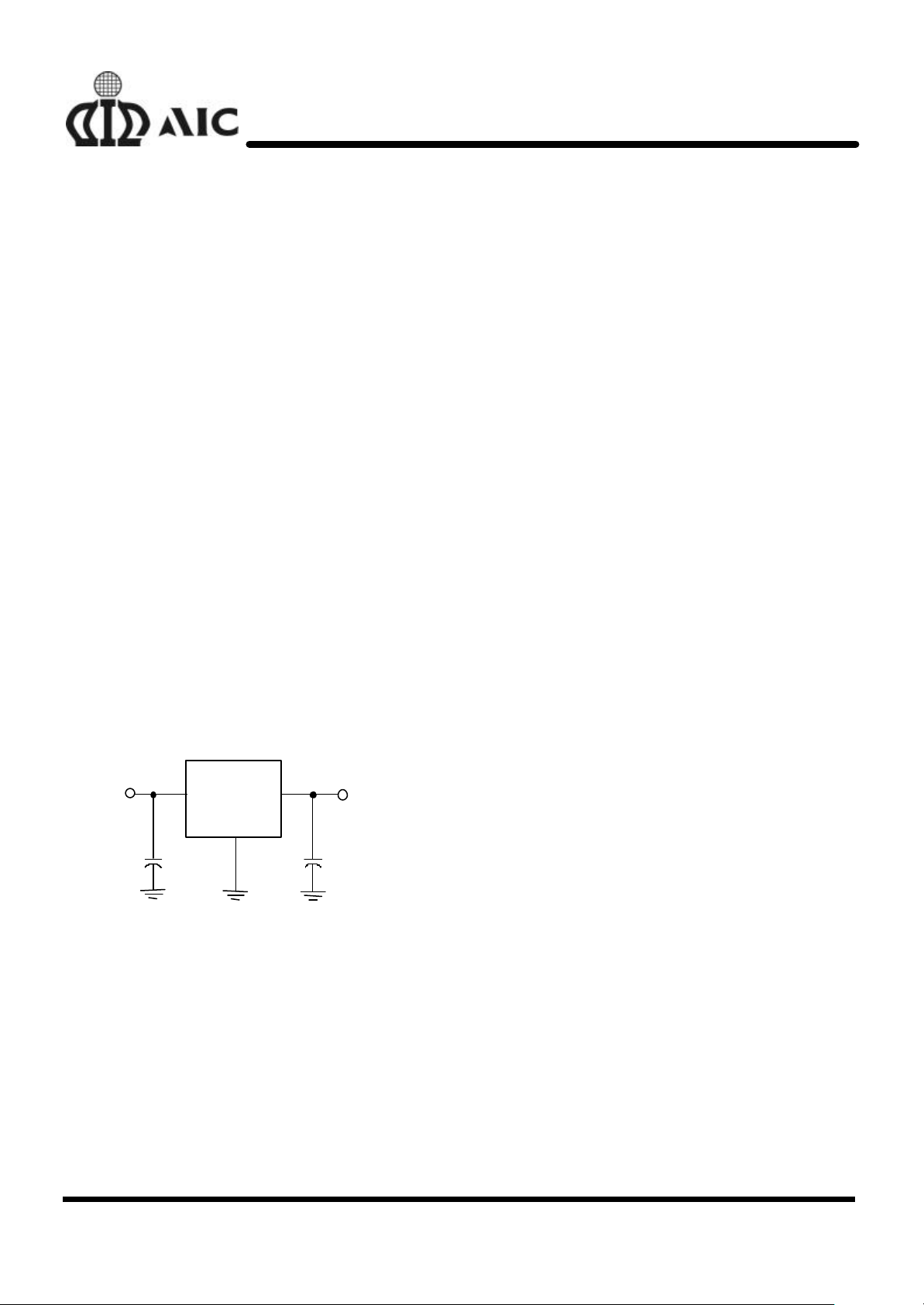
TYPICAL APPLICATION CIRCUIT
n
VOUT
++
VOUT
10µF
COUT
VIN
VIN
1µF
CIN
GND
Low Dropout Linear Regulator
Analog Integrations Corporation 4F, 9, Industry E. 9th Rd, Science Based Industrial Park, Hsinchu Taiwan, ROC www.analog.com.tw
DS-1740-00 Aug 2, 00 TEL: 886-3-5772500 FAX: 886-3-5772510 2
ORDER NUMBER
PIN CONFIGURATION
231
231
231
AIC1740
n ORDERING INFORMATION
AIC1740-XCX
PACKAGING TYPE
E: TO-252
F: TO-251
Y: SOT-223
OUTPUT VOLTAGE
18: 1.8V
20: 2.0V
25: 2.5V
27: 2.7V
30: 3.0V
AIC1740-18CE
AIC1740-20CE
AIC1740-25CE
AIC1740-27CE
AIC1740-30CE
(TO-252)
AIC1740-18CF
AIC1740-20CF
AIC1740-25CF
AIC1740-27CF
AIC1740-30CF
(TO-251)
FRONT VIEW
1: VOUT
2: GND
3: VIN
FRONT VIEW
1: VOUT
2: GND
3: VIN
AIC1740-18CY
AIC1740-20CY
AIC1740-25CY
AIC1740-27CY
AIC1740-30CY
(SOT-223)
n ABSOLUTE MAXIMUM RATINGS
Input Supply Voltage ...................................………….................................... -0.3~12V
Operating Junction Temperature Range .......……….............................. -40°C~ 85°C
Storage Temperature Range .........................………….......................... -65°C~150°C
Power Dissipation ....…………………………………..……………..……............... 0.85W
Thermal Resistance θJC TO-251, TO-252 Package ....…….…….......... 12.5°C/W
SOT-223 Package ....…………..……….............15°C/W
n TEST CIRCUIT
Refer to the TYPICAL APPLICATION CIRCUIT
FRONT VIEW
1: VOUT
2: GND
3: VIN
2
AIC1740
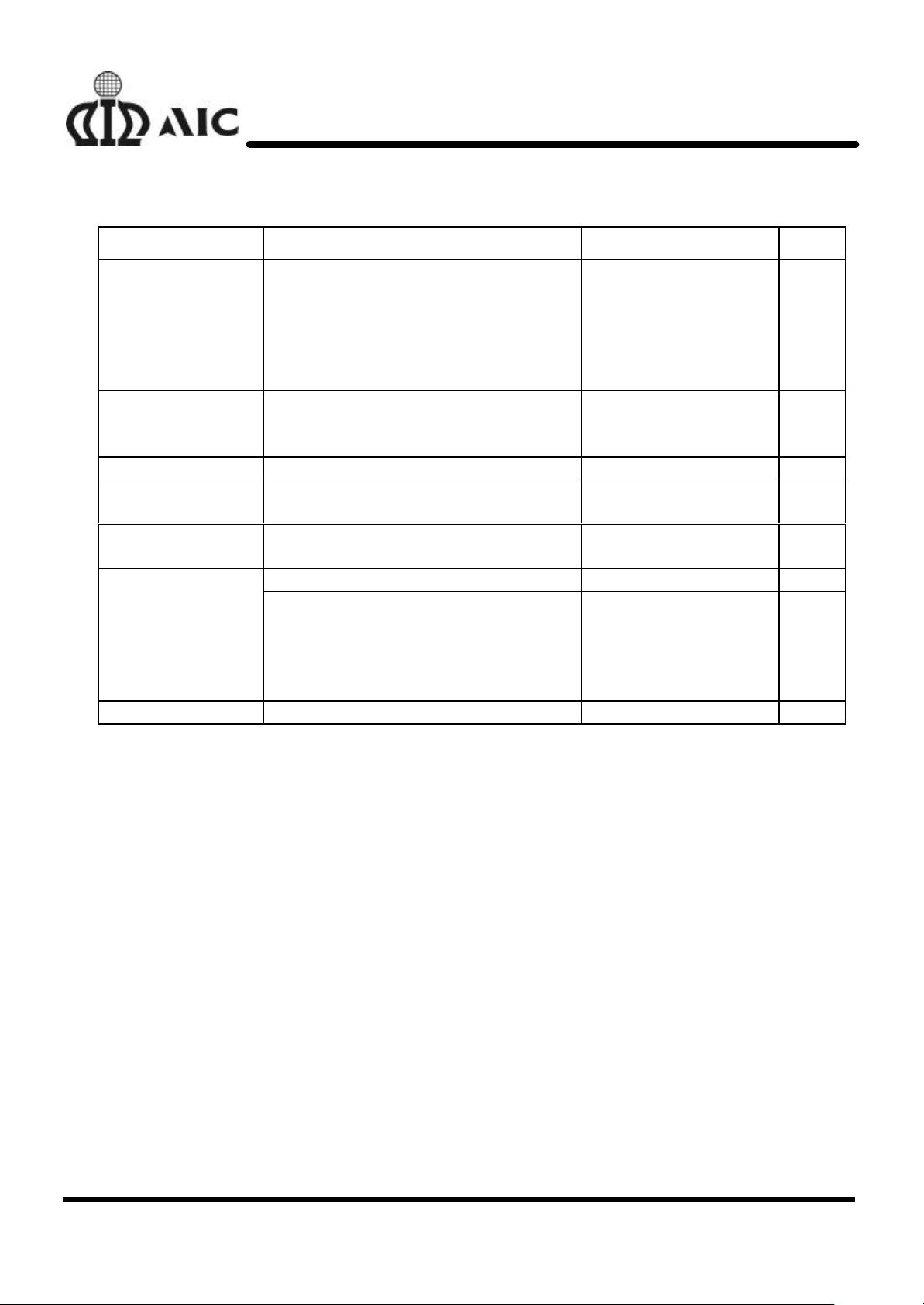
n ELECTRICAL CHARACTERISTICS (Ta=25°C, C
specified.)
PARAMETER TEST CONDITIONS MIN. TYP. MAX. UNIT
Output Voltage No Load
AIC1740-30
AIC1740-27
AIC1740-25
AIC1740-20
AIC1740-18
Output Voltage
Temperature
Coefficiency
Line Regulation IL=1mA, VIN=4.0~12V 3 10 mV
Load Regulation
(Note 2)
Current Limit
(Note 3)
(Note 4)
Ground Current IO=0.1mA~I
Note 1: Guaranteed by design.
Note 2: Regulation is measured at constant junction temperature, using pulse testing with a low ON time.
Note 3: Current limit is measured by pulsing a short time.
Note 4: Dropout voltage is defined as the input to output differential at which the output voltage drops 100mV
below the value measured with a 1V differential.
(Note 1) 50
VIN=5V, IL=0.1~500mA 20 50
VIN=5V, V
AIC1740s IL=0.1mA 0.2 10 mVDropout Voltage
AIC1740-30
AIC1740-27
AIC1740-25
AIC1740-20
AIC1740-18
=0V 650
OUT
, VIN=4V~12V 65 90 µA
MAX
VIN=4.0~12V
VIN=4.0~12V
VIN=4.0~12V
VIN=4.0~12V
VIN=4.0~12V
IL=500mA 900
=1µF, C
IN
2.940
2.646
2.450
1.960
1.764
=10µF, unless otherwise
OUT
3.0
2.7
2.5
2.0
1.8
950
1000
1260
1370
3.060
2.754
2.550
2.040
1.836
1050
1100
1150
1410
1520
V
PPM/°C
mV
mA
mV
3
 Loading...