

AIC AIC1739-30CZT, AIC1739-30CZL, AIC1739-30CX, AIC1739-27CZT, AIC1739-27CZL Datasheet
...
µ
µ
AIC1739
VIN
AIC1739
300mA Low Dropout Linear Regulator
n FEATURES
l Low Dropout Voltage of 180mV at 100mA
Output Current (3.0V Output Version).
l Guaranteed 300mA Output Current.
l Internal 1.3Ω P-MOSFET Draws no Base
Current.
l Low Ground Current at 55
l 2% Accuracy Output Voltage of 1.8V/ 2.0V/
A.
2.5V/ 2.7V/ 3.0V.
l Input Voltage Range up to 12V .
l Needs only 1
l Current and Thermal Limiting.
F for Stability.
n APPLICATIONS
l Voltage Regulator for CD-ROM Drivers.
l Voltage Regulator for LAN Cards.
l Voltage Regulator for Microprocessor.
l Wireless Communication Systems.
l Battery Powered Systems.
n DESCRIPTION
The AIC1739 is a 3-pin low dropout linear
regulator. The superior characteristics of the
AIC1739 include zero base current loss, very
low dropout voltage, and 2% accuracy output
voltage. Typical ground current remains
approximately 55µA, from no load to
maximum loading conditions. Dropout voltage
is exceptionally low. Output current limiting
and thermal limiting are built in to provide
maximal protection to the AIC1739 against
fault conditions.
The AIC1739 comes in the popular 3-pin
SOT-89 and TO-92 packages.
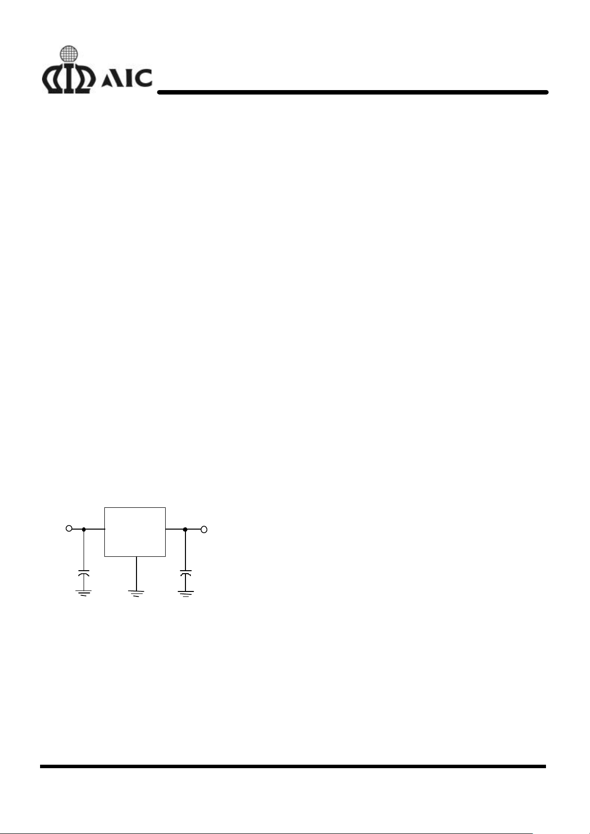
TYPICAL APPLICATION CIRCUIT
n
VOUT
V
IN
1µF
C
IN
GND
V
OUT
µ
F
10
C
OUT
Low Dropout Linear Regulator
Analog Integrations Corporation 4F, 9, Industry E. 9th Rd, Science Based Industrial Park, Hsinchu Taiwan, ROC www.analog.com.tw
DS-1739-01 TEL: 886-3-5772500 FAX: 886-3-5772510 1
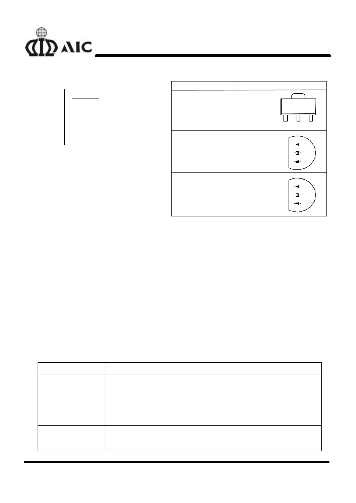
n ORDERING INFORMATION
AIC1739-XCX
PACKAGING TYPE
X: SOT89
ZT: TO92
ZL: TO92
ORDER NUMBER
AIC1739-18CX
AIC1739-20CX
AIC1739-25CX
AIC1739-27CX
AIC1739-30CX
(SOT-89)
AIC1739
PIN CONFIGURATION
FRONT VIEW
1: VOUT
2: GND
3: VIN
1 2 3
OUTPUT VOLTAGE
18: 1.8V
20: 2.0V
25: 2.5V
27: 2.7V
30: 3.0V
AIC1739-18CZT
AIC1739-20CZT
AIC1739-25CZT
AIC1739-27CZT
AIC1739-30CZT
(TO-92)
AIC1739-18CZL
AIC1739-20CZL
AIC1739-25CZL
AIC1739-27CZL
AIC1739-30CZL
(TO-92 L TYPE)
TOP VIEW
1: GND
2: VIN
3: VOUT
TOP VIEW
1: VIN
2: GND
3: VOUT
n ABSOLUTE MAXIMUM RATINGS
Input Supply Voltage ...................................................…………..…….................. -0.3~12V
Operating Junction Temperature Range .....………........…………................ -40°C~ 85 °C
Storage Temperature Range ....................……......................……….............. -65°C~150°C
Power Dissipation SOT-89 Package ....…...…................. 0.5W
TO-92 Package .....…………............. 0.5W
1
2
3
1
2
3
n TEST CIRCUIT
Refer to the TYPICAL APPLICATION CIRCUIT
n ELECTRICAL CHARACTERISTICS (Ta=25 °C, C
otherwise specified.)
PARAMETER TEST CONDITIONS MIN. TYP. MAX. UNIT
Output Voltage No Load
AIC1739-30
AIC1739-27
AIC1739-25
AIC1739-20
AIC1739-18
Output Voltage
(Note 1) 50
Temperature
Coefficiency
VIN=4.0~12V
VIN=4.0~12V
VIN=4.0~12V
VIN=4.0~12V
VIN=4.0~12V
=1µF, C
IN
2.940
2.646
2.550
1.960
1.764
=10µF, unless
OUT
3.000
2.700
2.500
2.000
1.800
3.060
2.754
2.550
2.040
1.836
150 PPM/°C
V
2
 Loading...