

AIC AIC1733 User Manual
µ
查询AIC1733-15CVBG供应商
AIC1733
500mA, Low Dropout Linear Regulator with Shutdown
FEATURES
Active Low Shutdown Control.
Very Low Quiescent Current.
Very Low Dropout Voltage of 650mV at 500mA
Output Current (3.0V Output Version)
1.5V, 1.8V, 2.5V, 2.8V, 3.0V, 3.3V Output Voltage.
Short Circuit and Thermal Protection.
±2% Output Tolerance.
Miniature Package: SOT-23-5
APPLICATIONS
PDA
DSC
Notebook
Pagers
Personal Communication Equipment
Cordless Telephones
Portable Instrumentation
Portable Consumer Equipment
Battery Powered Systems
DESCRIPTION
AIC1733 is a 500mA low noise, low dropout
linear regulator, and is housed in small SOT-23-5
package. The device is in the “ON” state when
the
SHDN pin is set to logic high level. An
internal P-MOSFET pass transistor is used to
achieve 650mV low dropout voltage at 500mA
load current. It offers high precision output
voltage of ±2%. The quality of low quiescent
current and low dropout voltage makes this
device ideal for battery power applications. The
internal reverse bias protection eliminates the
requirement for a reverse voltage protection
diode. The high ripple rejection and low noise of
AIC1733 provide enhanced performance for
critical applications. The noise bypass pin can be
connected an external capacitor to reduce the
output noise level.
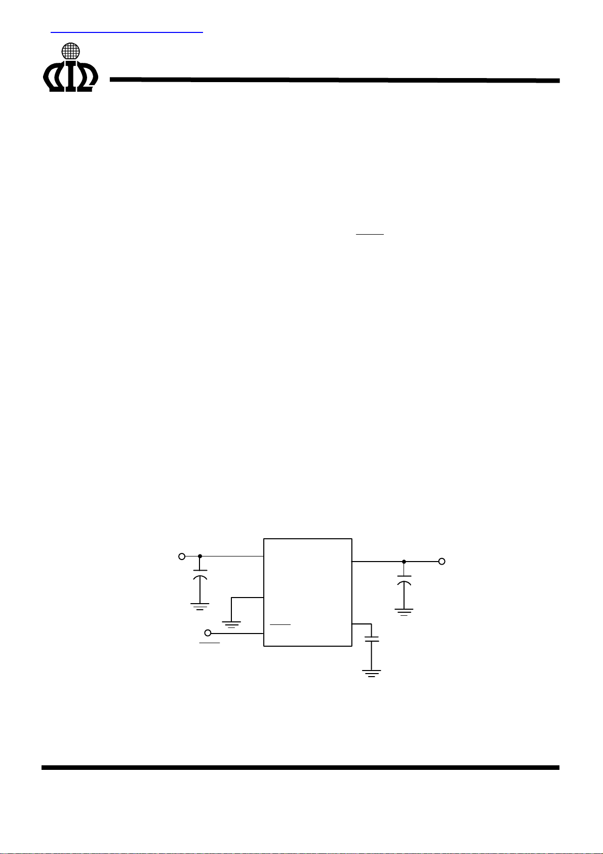
TYPICAL APPLICATION CIRCUIT
V
IN
+
C
IN
1
F
V
SHDN
Low Noise Low Dropout Linear Regulator
Analog Integrations Corporation Si-Soft Research Center DS-1733P-03 092304
3A1, No.1, Li-Hsin Rd. I , Science Park , Hsinchu 300, Taiwan , R.O.C.
TEL: 886-3-5772500 FAX: 886-3-5772510 www.analog.com.tw
VIN
GND
SHDN
AIC1733
VOUT
BP
C
BP
0.1µF
V
+
C
OUT
1µF
OUT
1
AIC1733
ORDERING INFORMATION
AIC1733-XXXXXX
PACKING TYPE
TR: TAPE & REEL
BG: BAG
PACKAGE TYPE
V: SOT-23-5
C: COMMERCIAL
P: LEAD FREE COMMERCIAL
OUTPUT VOLTAGE
15: 1.5V
18: 1.8V
25: 2.5V
28: 2.8V
30: 3.0V
33: 3.3V
(Of a unit of 0.1V within the voltage range from 1.5V to 3.3V, additional
voltage versions for this product line may be available on demand with
prior consultation with AIC.)
Example: AIC1733-18CVTR
1.8V Version, in SOT-23-5 Package & Tape & Reel
Packing Type
AIC1733-18PVTR
1.8V Version, in SOT-23-5 Lead Free Package & Tape &
Reel Packing Type
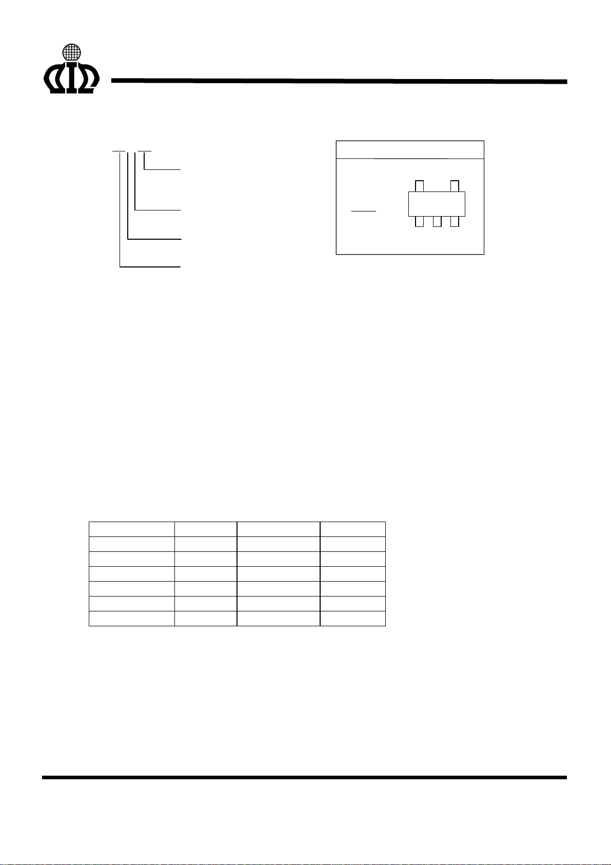
• SOT-23-5 Marking
Part No. Marking Part No. Marking
AIC1733-15CV EE15 AIC1733-15PV EE15P
AIC1733-18CV EE18 AIC1733-18PV EE18P
AIC1733-25CV EE25 AIC1733-25PV EE25P
AIC1733-28CV EE28 AIC1733-28PV EE28P
AIC1733-30CV EE30 AIC1733-30PV EE30P
AIC1733-33CV EE33 AIC1733-33PV EE33P
PIN CONFIGURATION
SOT-23-5 (CV)
TOP VIEW
1: VIN
2: GND
3: SHDN
4: BP
5: VOUT
5
1
4
2
3
2
AIC1733
ABSOLUTE MAXIMUM RATINGS
Supply Voltage .................………………………………..…………………....................12V
Shutdown Terminal Voltage ..………………………………………………………..............12V
Noise Bypass Terminal Voltage .…………………………….………………………..............5V
Operating Temperature Range .………………………………………………….....-40ºC~85ºC
Maximum Junction Temperature
Storage Temperature Range ................…………………………………….........-65ºC~150ºC
Lead Temperature (Soldering, 10 sec)
Thermal Resistance (Junction to Case) SOT-23-5 …....………..………..………..130°C /W
Thermal Resistance Junction to Ambient SOT-23-5 …....……..…………..………..220°C /W
(Assume no ambient airflow, no heatsink)
Absolute Maximum Ratings are those values beyond which the life of a device may be impaired.
125°C
260°C
TEST CIRCUIT
Refer to TYPICAL APPLICATION CIRCUIT.
3
AIC1733
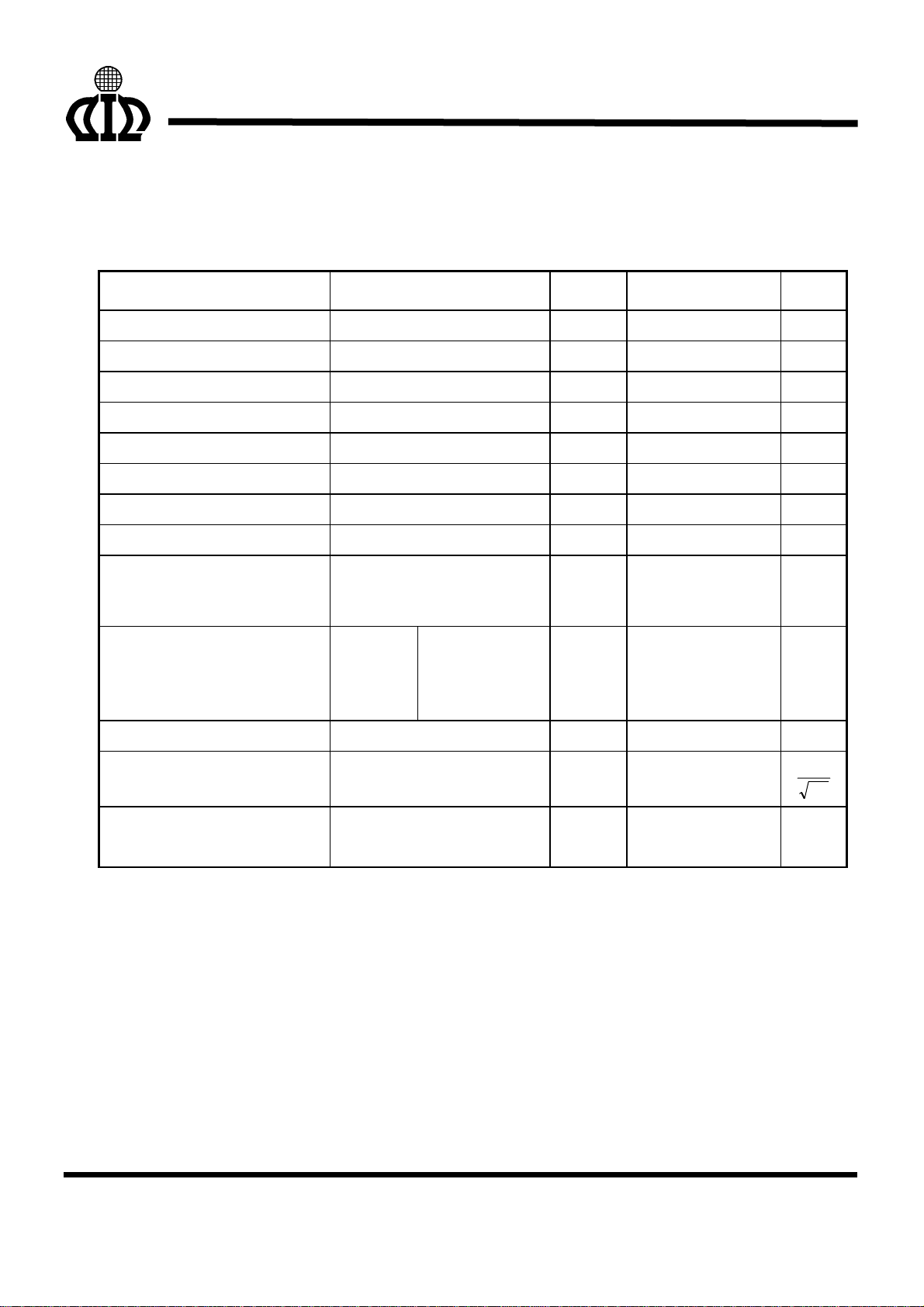
ELECTRICAL CHARACTERISTICS
=1µF, C
(C
IN
PARAMETER TEST CONDITIONS SYMBOL MIN. TYP. MAX. UNIT
Quiescent Current I
Standby Current VIN = 3.6~7V, output OFF I
GND Pin Current I
Continuous Output Current VIN = 5V I
Output Current Limit VIN = 5V, V
Output Voltage Tolerance VIN = 5V, no load V
Temperature Coefficient TC 50 150
Line Regulation
Load Regulation
Dropout Voltage
Noise Bypass Terminal Voltage
=4.7µF, TJ=25°C, unless otherwise specified)
OUT
= 0mA, VIN = 3.6~7V IQ 40 55
OUT
= 0.1~500mA I
OUT
= 0V IIL
OUT
VIN = V
V
V
I
OUT(TYP)
= V
IN
OUT
= V
IN
OUT
= 0.1~500mA
OUT
=500mA
I
L
+ 1V to 7V
+ 1.2V (Vout≥ 2.5V)
+ 1.8V (Vout≤ 2.4V)
3.0V≤V
2.5V≤V
2.0V≤V
1.5V≤V
OUT
OUT
OUT
OUT
≤3.3V
≤2.9V
≤2.4V
≤1.9V
V
0.1
STBY
30 50
GND
OUT
500 mA
500 600 mA
∆V
OUT
LIR
-2 2 %
∆V
LOR
V
DROP
1.23
REF
µA
µA
µA
ppm/ºC
3 10 mV
20 40
650
780
1100
1400
1050
1180
1500
1800
mV
mV
V
Output Noise CBP = 0.1µF, f = 1KHz,VIN = 5V ∆n 0.46
Ripple Rejection
f = 1KHz, Ripple = 0.5V
C
= 0.1µF
BP
P-P
,
RR 55
V
µ
Hz
dB
4
 Loading...