

AIC AIC1714-50CZ, AIC1714-50CX, AIC1714-33CZ, AIC1714-33CX, AIC1714-30CZ Datasheet
...
AIC1714
µ
Negative Voltage Regulator
FEATURES
Low Power Consumption.
Low Temperature Coefficient.
Output Short Circuit Protected.
Wide Operating Voltage Range.
Good Input Stability.
Space-Saving Package: TO-92 or SOT-89
APPLICATIONS
LCD for Printing Calculators
Cameras
Voltage References for Instrumentation
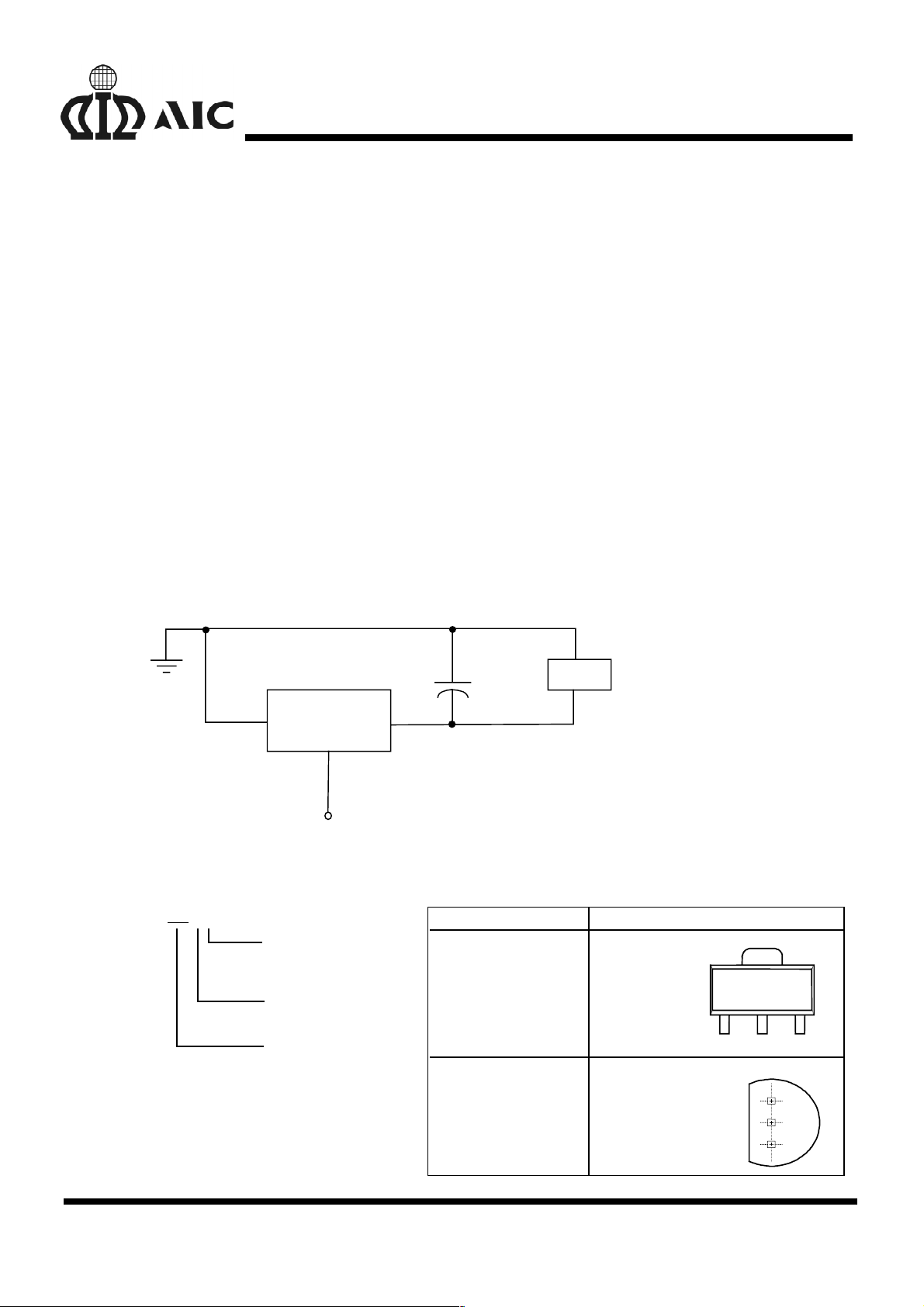
TYPICAL APPLICATION CIRCUIT
1
+
F
DESCRIPTION
The AIC1714 is a series of 3-terminal negative
voltage regulators with output voltages
internally set below the positive supply voltage.
Since the AIC1714 consumes less current and
only requires a small input/output voltage
difference than existing industry standard 3-
terminal voltage regulators, a battery-powered
portable equipment is afforded a high capacity
and longer service life. The AIC1714 is ideal for
power source of liquid crystal displays.
LOAD
AIC1714
GND
VIN
-6.0V
Negative Voltage Regulator
ORDERING INFORMATION
AIC1714-XX-XX
PACKAGING TYPE
X: SOT-89
Z: TO-92
TEMPERATURE RANGE
C: 0°C~+70°C
OUTPUT VOLTAGE
30: -3.0V
33: -3.3V
50: -5.0V
OUT
ORDER NUMBER
AIC1714-30CX
AIC1714-33CX
AIC1714-50CX
(SOT-89)
AIC1714-30CZ
AIC1714-33CZ
AIC1714-50CZ
(TO-92)
PIN CONFIGURATION
FRONT VIEW
1: VIN
2: GND
3: VOUT
TOP VIEW
1: GND
2: VIN
3: VOUT
123
1
2
3
Analog Integrations Corporation 4F, 9, Industry E. 9th Rd, Science Based Industrial Park, Hsinchu Taiwan, ROC www.analog.com.tw
DS-1714-02 TEL: 886-3-5772500 FAX: 886-3-5772510
1
ABSOLUTE MAXIMUM RATINGS
A
A
_
Supply Voltage .................................................………................................ -13V
AIC1714
Operating Temperature Range
Storage Temperature Range
.........................………........................ - 20°C~80°C
........................………......................... - 65°C~150°C
Power Dissipation SOT-89 Package
TO-92 Package
TEST CIRCUIT
I
IN
+
Voltage
Source
GND
AIC1714
V
OUT
-
V
IN
V
+
VIN
ELECTRICAL CHARACTERISTICS (V
specified.)
PARAMETER TEST CONDITIONS SYMBOL MIN. TYP. MAX. UNIT
.....….............. 0. 80W
........…............ 0.78W
I
OUT
+
V
OUT
+
= -6.0V, Ta=25°°°°C, unless otherwise
IN
1µF
LOAD
Output Voltage I
=300µA AIC1714-30 V
OUT
OUT
-2.95 -3.0 -3.05 V
AIC1714-33 -3.25 -3.3 -3.35 V
AIC1714-50 -4.93 -5.0 -5.07 V
Load Regulation I
I/O Voltage Difference I
Supply Current I
Input Stability
Temperature Coefficient -25°C~85°C T
Output Short Circuit Current R
=0~5mA ∆V
OUT
=300µA V
OUT
=0 I
OUT
=0 15 24 mA
LOAD
OUT
DIFF
IN
∆
V
OUT
∆
•
VV
IN OUT
C
20 100
50 200
6 12
0.05
50 ppm
mV
mV
µA
%/ V
2
 Loading...