

AIC AIC1686 Datasheet

AIC1686
Off-Line Power Supply Protection IC with Shunt
Regulator
FEATURES
Overvoltage Protection for 3.3V, 5V, and 12V
Outputs.
Power Good Signal for 5V Output.
Remote ON/OFF Input.
Uncommitted Protection Input.
5V Regulator with 25mA Source Current.
2.5V Precision Shunt Regulator.
8V to 16V Operation.
Low Power Consumption.
APPLICATIONS
PC Off-Line Power Management.
DESCRIPTION
The AIC1686 is a supervisory and protection IC
intended for use in off-line, multiple output
power supplies. It consists of protection circuitry,
power good indicator, remote ON/OFF control,
and precision shunt regulator. The overvoltage
protection (OVP) function is for 3.3V, 5V, and
12V outputs. In addition, an uncommitted fault
detection input (PRIN) is available for use with
other protection functions, such as overcurrent,
undervoltage, and/or short-circuit protection of
outputs.
The shunt regulator has been included to
implement the feedback control for one of the
power supply’s outputs. The noniverting input
(EAI) is internally tied to a precision 2.5V
reference.
The power good circuit monitors the 5V output
and asserts, with a programmable delay, a TTL
compatible high logic level at its output after the
5V output reaches the regulation range. The
delay is programmed by a timing capacitor
connected to CPG pin of the IC. The power
good circuit sets its output low before the 5V
output goes out of regulation range. The remote
ON/OFF function enables the power supply to
be turned on and off from the secondary side by
a switch.
Analog Integrations Corporation 4F, 9, Industry E. 9th Rd, Science Based Industrial Park, Hsinchu Taiwan, ROC www.analog.com.tw
DS-1686-00 TEL: 886-3-5772500 FAX: 886-3-5772510
1
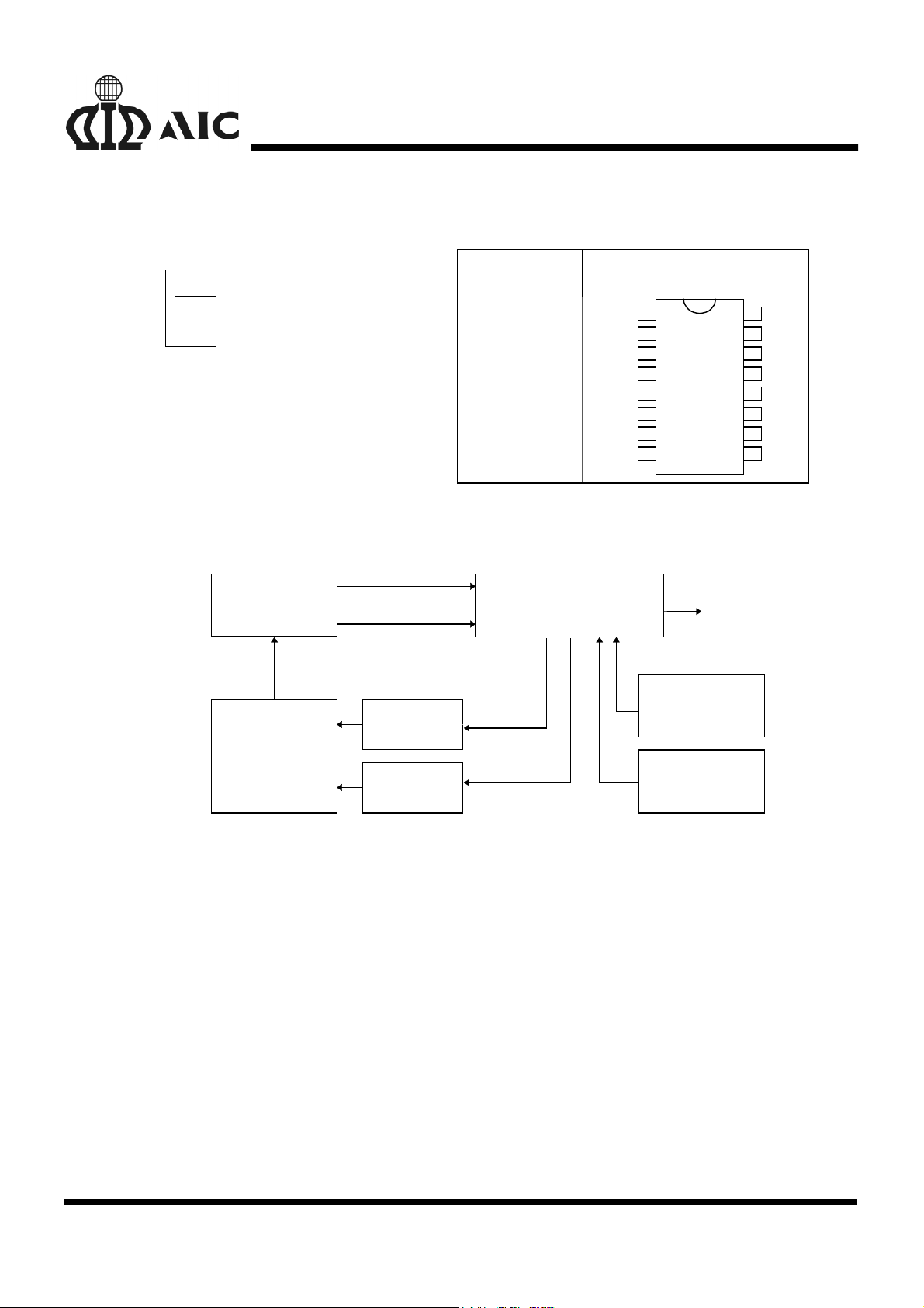
ORDERING INFORMATION
AIC1686
AIC1686 XX
PACKAGE TYPE
N: PLASTIC DIP
TEMPERATURE RANGE
C: 0°C~70°C
TYPICAL APPLICATION CIRCUIT
DC OUTPUTS
AC/DC
CONVERTER
PWM
CONTROLLER
AC LINE SENSE
OPTO-
ISOLATOR
OPTP-
ISOLATOR
ORDER NUMBER
AIC1686CN
(PLASTIC DIP)
AIC1686
REGULATION
PROTECTION O/P
PIN CONFIGURATION
TOP VIEW
1
PRIN
2
REMI
PG
3
V33
4
GND
5
V5
6
V12
7
8
EAO
PROTECTION
INPUT
REMOTE
ON/OFF
16
15
14
13
12
11
10
9
POWER
GOOD
CPG
FL
REMO
REF
VCC
CLS
LS
EAI
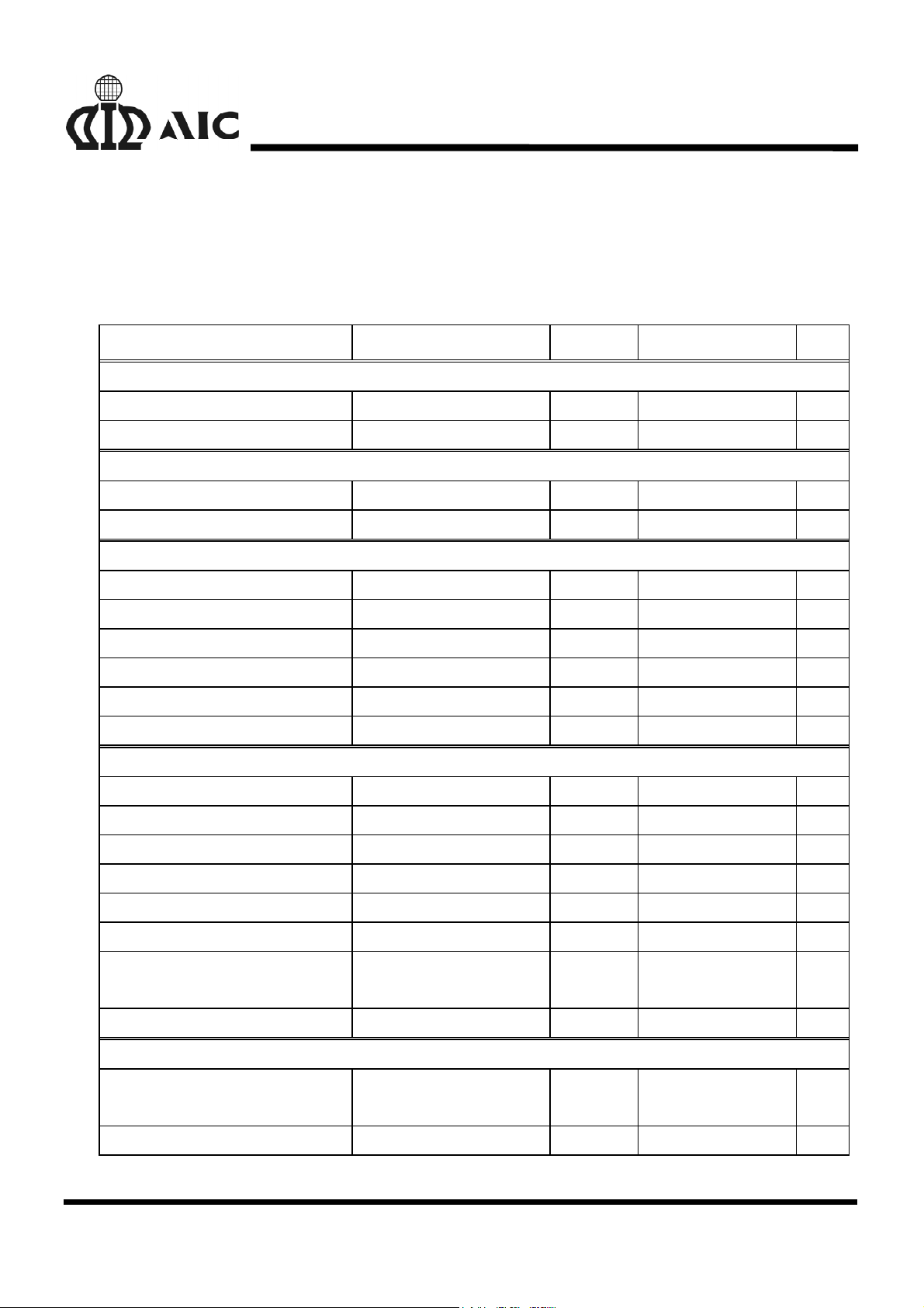
ABSOLUTE MAXIMUM RATINGS
Supply Voltage, VCC .......................……………………..………..….................-0.5V to 16V
Pins: V12, V5, V33, LS, EAO ....................…….………….…………................. -0.5V to 16V
Any Other Pins ...............…………........………….…................. GND - 0.5V to VCC+0.5V
Ambient Temperature Range .......................………………………..…................. 0°C~70°C
Thermal Information
Thermal Resistance, θ
Maximum Junction Temperature (Plastic Package) .....….......................………....... 125°C
Maximum Storage Temperature Range .......................……........………....... -65°C~150°C
Maximum Lead Temperature (Soldering 10 Sec) .......................……………............. 300°C
Maximum Power Dissipation .......................………………………………................. 500mW
(Derate at 10mW/°C above 70°C ambient)
DIP Package ...................………..…................. 110°C/W
JA
2
TEST CIRCUIT
Refer to TYPICAL APPLICATION CIRCUIT.
AIC1686
ELECTRICAL CHARACTERISTICS (VCC= 12V, Ta=25°
°C, unless otherwise specified.)
°°
PARAMETER TEST CONDITIONS SYMBOL MIN. TYP. MAX. UNIT
VCC Supply Current
Nominal Mode ( Remote On) All Outputs Unloaded I
Standby Mode ( Remote Off) All Outputs Unloaded I
VCC
VCCSB
5V Reference (Note1)
Reference Voltage IO=0 to 25mA, CL=1µFV
REF
4.85 5 5.15 V
Line Regulation VCC=8V to 16V, CL=1µF15mV
Error Amplifier
Internal Reference Voltage V
Maximum Output Sink Current V
=1V I
EAO
EA
EA
2.45 2.5 2.55 V
20 mA
Open Loop Voltage Gain 80 dB
Unity Gain Bandwidth CL=100pF GBW 3 MHz
Power Supply Rejection Ratio PSRR 85 dB
Slew Rate CL=100pF SR 2 V/µS
0.5 1 mA
0.4 0.8 mA
Fault Detection
Fault Output High Voltage IOH=500µA, Remote On V
Fault Output High Voltage IOH=20µA, Remote Off V
Fault Output Low Voltage IOL=4.5mA V
FLOH
FLOHS
FLOL
3.3V Input OVP Trip Level Input Voltage Rising V33
5V Input OVP Trip Level Input Voltage Rising V5
OVP
12V Input OVP Trip Level Input Voltage Rising V12
Protection Input Trip Level
Input Voltage Rising
Input Voltage Falling
Fault Latch Delay T
V
PIH
V
PIL
FL
Remote ON/OFF
REMI Input Threshold Input Voltage Rising
Input Voltage Falling
V
RIH
V
RIL
REMI Input Hysteresis HYS
OVP
OVP
4V
4V
3.744.3V
5.566.5V
13.2 14 15.6 V
3.8
10 25 50 µS
3.8
RI
0.7 1.8 V
0.4 V
1.2
1.2
V
V
V
V
3
 Loading...