

AIC AIC1680P16CX, AIC1680P16CV, AIC1680P16CU, AIC1680N60CZ, AIC1680N60CX Datasheet
...
AIC1680
Ultra Low Power Voltage Detector
Analog Integrations Corporation 4F, 9, Industry E. 9th Rd, Science Based Industrial Park, Hsinchu Taiwan, ROC www.analog.com.tw
DS-1680-00 Dec 29, 00 TEL: 886-3-5772500 FAX: 886-3-5772510
1
FEATURES
Ultra-Low Quiescent Current.
1.5V to 10.0V Input Voltage Operation.
Flexible Detection Voltage Setting
0.1V Step in the Range of 1.6V to 6.0V
High Detection Voltage Accuracy at ±2.5%.
Built-In Detection Voltage Hysteresis.
Three Output Types: N-ch, P-ch and CMOS.
Space Saving Packages: TO-92, SOT-89,
SOT-23 and SOT23-5.
APPLICATIONS
Battery Checker for Battery-Operated Systems.
CPU & Logic Circuit Reset.
Memory Back-up Circuit.
Level Discriminator.
Power Failure Detector.
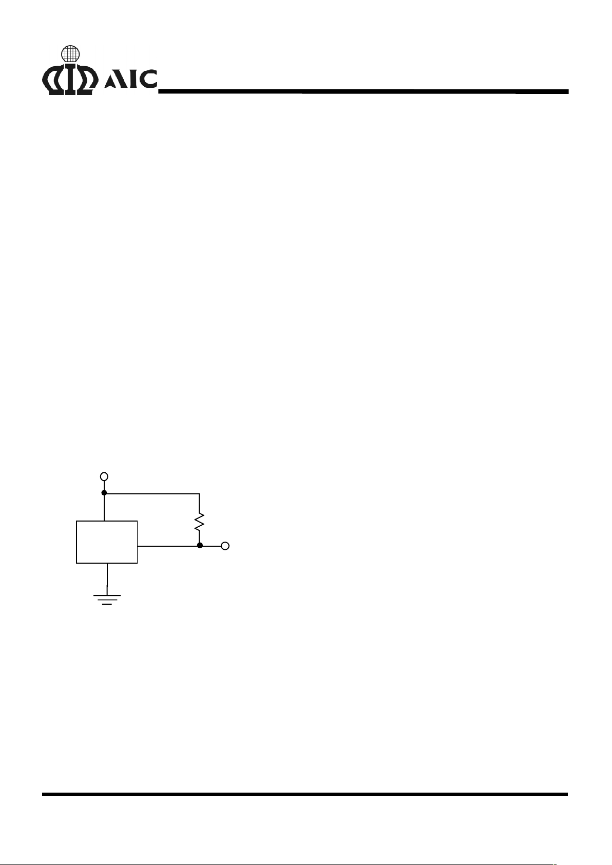
TYPICAL APPLICATION CIRCUIT
100K
A
IC1680N
V
OUT
V
IN
VOUT
GND
VDD
Voltage Level Indicator (N-ch Open-Drain Output)
DESCRIPTION
The AIC1680 is an accurate, ultra-low power
consumption voltage detector IC, fabricated with
advanced CMOS process. The AIC1680 con-
sists of a comparator, a voltage reference unit,
a resistor divider, two output drivers, and a
hysteresis circuit.
The consumption current is so low that it can
often be ignored when compared to the battery
self-discharge current. The values of detection
and hysteresis voltage are set internally and are
accurately controlled by trimming techniques.
There are three types of output: N-ch open-
drain, P-ch open-drain, and CMOS. Four types
of package, TO-92, SOT-89, SOT-23 and SOT-
23-5, are available to save board space.
AIC1680
2
ORDERING
INFORMATION
ORDER NUMBER
AIC1680CU
(SOT-23)
PIN CONFIGURATION
FRONT VIEW
1: VOUT
2: VDD
3: GND
1
2
3
1
2
3
PACKAGING TYPE
U: SOT-23
X: SOT-89
Z: TO-92
V:SOT23-5
AIC1680CZ
(TO-92)
FRONT VIEW
1: VOUT
2: VDD
3: GND
DETECTION VOLTAGE OPTIONAL
16: 1.6V
17: 1.7V
:
:
60: 6.0V
OUTPUT TYPE
N: N-ch Open Drain
P: P-ch Open Drain
C: CMOS
A
IC1680XXXCX
AIC1680CX
(SOT-89)
123
FRONT VIEW
1: VOUT
2: VDD
3: GND
1
45
(MARK SIDE)
FRONT VIEW
1: VOUT
2: VDD
3: GND
4: NC
5: NC
AIC1680CV
(SOT-23-5)
23
ABSOLUTE MAXIMUM RATINS
Supply Voltage ...........................………………….....…….....…………............................ 10V
Output Voltage ……………………………………………………………………..Vss-0.3 to 10V
Operating Temperature Range ……….……...................………...................... -30°C ~ 80°C
Storage Temperature Range ...........…….....................…………................. - 65°C ~ 150°C
Lead Temperature (Soldering) 10 sec. ...........…..........………............………...….......260°C
Output Current ...........…..........……….…………………………...........………...….......20mA
AIC1680
3
ELECTRICAL CHARACTERISTICS (Test Conditions : Ta=25°
°°
°C )
SYMBOL PARAMETER TEST CONDITIONS MIN TYP MAX UNIT
V
DET
Detector Voltage 0.975 1.0 1.025 V
DET
V
HYS
Detector Threshold Hysteresis 0.03 0.05 0.07 V
DET
I
DD
Supply Current VDD=2.0V
V
DD
=3.0V
V
DD
=4.5V
V
DD
=6.0V
V
DD
=10.0V
0.7
0.9
1.3
1.8
3.2
1.1
1.5
2.0
2.7
4.8
µA
V
DD
Operation Voltage 1.5 10 V
I
OUT
(Nch) Output Current VDS=0.5V VDD=2.4V
V
DS
=0.5V VDD=3.6V
V
DS
=0.5V VDD=4.6V
V
DS
=0.5V VDD=6.0V
3.24
5.85
7.74
10.44
mA
I
OUT
(Pch) Output Current VDS=-2.1V VDD=4.5V 3.5 mA
Temperature Coeficience ±150 ppm/°C
T
DELAY
Output Delay Time 200 µS
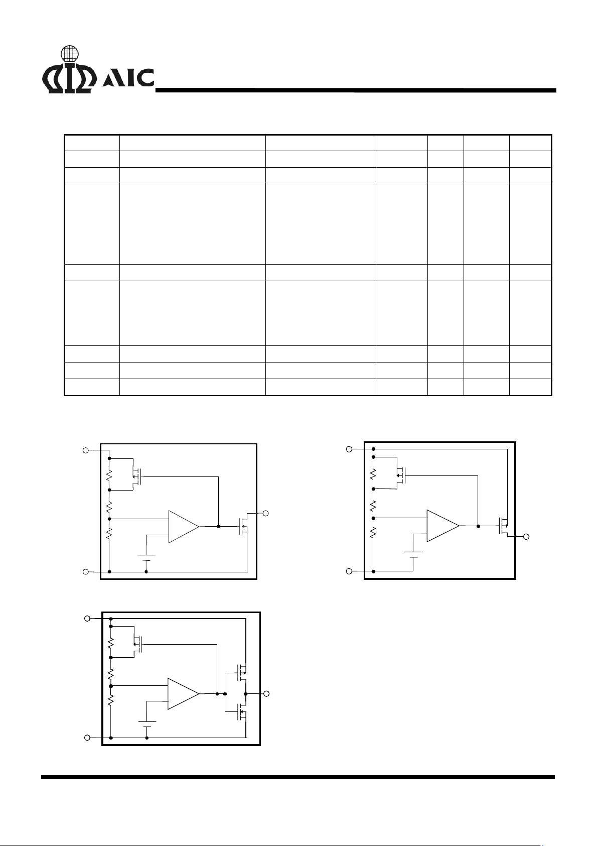
BLOCK DIAGRAM
VOUT
VDD
GND
1.25V
-
+
VOUT
VDD
-
+
GND
1.25V
N-ch open drain output P-ch open drain output
-
+
VD D
VOU T
GND
1.25V
CMOS output
 Loading...