

AIC AIC1660CS, AIC1660 Datasheet
AIC1660
µ
Switched-Capacitor Voltage Converter
n FEATURES
l Lowest Output Impedance (Typical 35Ω at
VIN=5V).
l Improved Direct Replacement for 7660.
l 1.5V to 6V Operation.
l No External Diode Required.
l Simple Conversion of +5V to -5V.
l Low Quiescent Current (Typical 36
l High Power Efficiency (Typical 98%)
l Boost Pin for Higher Switching Frequency.
l Improved SCR Latchup Protection.
A at VIN=5V).
n APPLICATIONS
l RS-232 Power Supplies.
l Handheld Instruments.
l Data Acquisition Systems.
l Supply Splitter, V
l Operational Amplifier Supplies.
l Panel Meter.
OUT
= ±V
IN
/2.
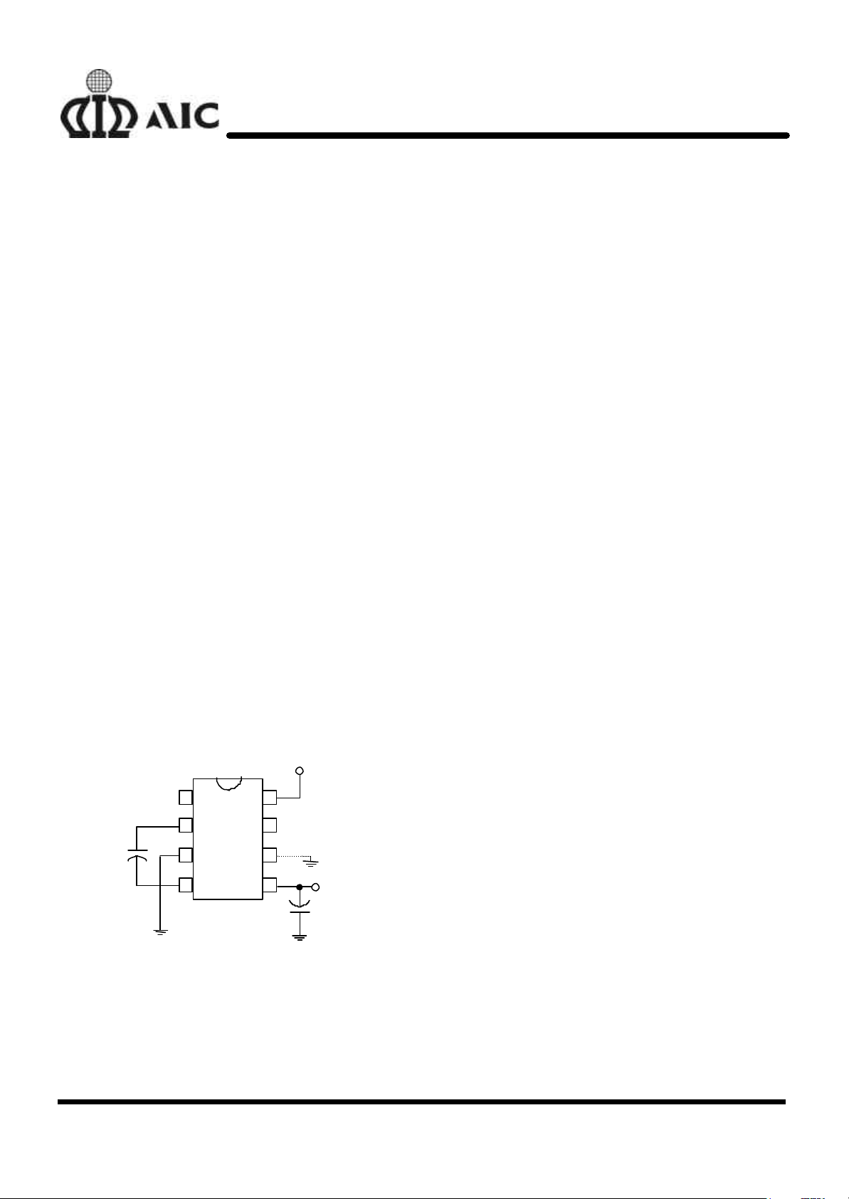
n TYPICAL APPLICATION CIRCUIT
IN
V
(1.5V to 6V)
1 8
Required for
7
6
5
≤
IN
V
3V
V
=-V
OUT
IN
10µF
+
C2
10µF
C1
2
+
AIC1660
3
4
n DESCRIPTION
The AIC1660 is a monolithic CMOS switched
capacitor voltage converter. Designed to be an
improved direct replacement for the popular 7660
and LTC1044, the main function of the AIC1660 is
to convert a positive input voltage in the range of
1.5V to 6V to the corresponding negative output
voltage in the range of -1.5V to -6V. The input
voltage can also be doubled (V
divided (V
±nV
), as shown in application examples.
IN
OUT
= V
/2 ), or multiplied (V
IN
The chip contains a series DC power supply
regulator, oscillator, control circuitry and four
output power MOS switches. The frequency of
oscillator can be lowered by the addition of an
external capacitor to the OSC pin, or the oscillator
may be over-driven by an external clock.
The boost function is available to raise the
oscillator frequency to optimize performance in
specific applications. The “LV” terminal may be
tied to GND to improve low input voltage (V
≤3V) operation, or be left floating for input voltage
larger than 3V to improve power dissipation.
The AIC1660 provides performance superior to
previous designs by combining low output
impedance, low quiescent current with high
efficiency, and by eliminating diode drop voltage
losses. The only required external components
are two low cost electrolytic capacitors.
OUT
= 2V
OUT
IN
),
=
IN
Negative Voltage Converter
Analog Integrations Corporation 4F, 9, Industry E. 9th Rd, Science Based Industrial Park, Hsinchu Taiwan, ROC www.analog.com.tw
DS-1660T-P4 Oct. 4, 01 TEL: 886-3-5772500 FAX: 886-3-5772510 1
n ORDERING INFORMATION
C
10µF
AIC1660 CX
AIC1660
ORDER NUMBER PIN CONFIGURATION
PACKAGE TYPE
N: PLASTIC DIP
S: SMALL OUTLINE
AIC1660CN
(PLASTIC DIP)
AIC1660CS
(PLASTIC SO)
TOP VIEW
BOOST
CAP+
GND
CAP-
1
2
3
4
n ABSOLUTE MAXIMUM RATINGS
Supply Voltage .............………………............……………………....................................................... 6.0V
Input Voltage on Pin 1, 6 and 7 ...…………….......................... …………………............. -0.3V ~VIN + 0.3V
Operating Temperature Range ........…………................……………….…….......……........... -40°C~+85°C
Storage Temperature Range..........…………...................……………………........................ -65°C~150°C
n TEST CIRCUIT
S
I
R
10µF
BOOST
1
2
CAP+
+
C1
GND
3
VIN
OSC
LV
8
7
OSCAIC1660
6
External
Oscillator
VIN
8
OSC
7
LV
6
VOUT
5
VIN
IL
L
4
CAP-
VOUT
5
C2
VOUT
+
2
AIC1660
µ
Supply Voltage (V)
Fig.
2 Power Efficiency
vs.
Load Current
n ELECTRICAL CHARACTERISTICS (V
unless otherwise specified.)
PARAMETER TEST CONDITIONS SYMBOL MIN TYP MAX UNIT
Supply Current RL = ∞ I
Minimum Supply Voltage RL = ∞ V
Maximum Supply Voltage RL = ∞ V
Output Resistance IL =20mA,
F
=10KHz
OSC
Oscillator Frequency C
Power Efficiency RL= 5K, F
Voltage Conversion Efficiency RL = ∞ V
=0
OSC
Pin 1 Floating or GND
Pin 1=V
IN
=10KHz P
OSC
=5.0V, TA=25°C, OSC=free running,
IN
S
INL
INH
R
OUT
F
OSC
1.5 V
36 70 µA
35 70 Ω
10
50
EFF
OUTEFF
96 98 %
98 99.9 %
6 V
KHz
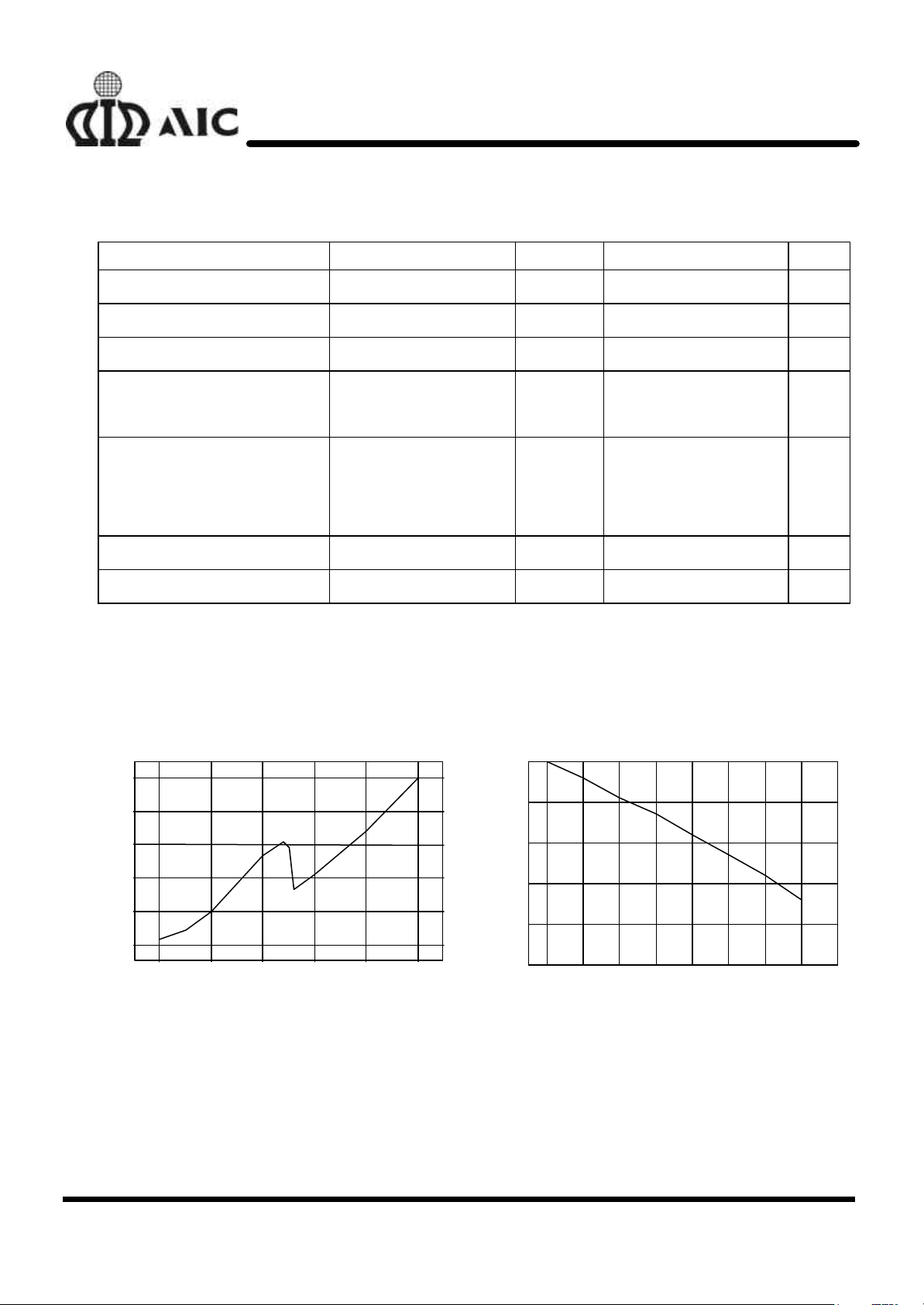
n TYPICAL PERFORMANCE CHARACTERISTICS (T
50
40
A)
30
20
10
Supply Current (
0
1 2 3 4 5 6
Fig. 1 Supply Current vs. Supply Voltage
100
90
80
70
60
Power Efficiency (%)
50
0 10 20 30 40 50 60 70 80
=25 °C)
A
Load Current (mA)
3
 Loading...