

AIC AIC1631, AIC1631CN, AIC1631ACS, AIC1631ACN, AIC16315CS Datasheet
...
AIC1631
2-Cell, 500mA, Step-Up DC/DC Converter
Analog Integrations Corporation 4F, 9, Industry E. 9th Rd, Science Based Industrial Park, Hsinchu Taiwan, ROC www.analog.com.tw
DS-1631-04 Dec 27, 00 TEL: 886-3-5772500 FAX: 886-3-5772510
1
FEATURES
High Efficiency 90%.
Adjustable Output Voltage with Two Resistors
(AIC1631A)
Power-Saving Shutdown Mode (7µA typical).
Internal 2A Switch.
120KHz Switching Rate.
Adjustable Switch Current Limit.
On-Chip Low Battery Detector.
APPLICATIONS
Palmtop & Notebook Computers.
Pocket Organizers.
Cameras.
Pagers.
Battery Backup Supplies.
Portable Instruments.
DESCRIPTION
The AIC1631 is a high efficiency step up DC-
DC converter. Only four external components
are required to deliver a fixed voltage of 3V,
3.3V, or 5V. The output voltage can be exter-
nally set to an arbitrary value below breakdown
voltage of the power switch for AIC1631A. Effi-
ciency beyond 87% can be easily achieved at
100mA load with 2.2V to 3V input voltages.
Logic-controlled shutdown mode is provided for
power saving. Switch current limit can be pro-
grammed with a resistor. The low battery de-
tector can be configured as a linear regulator or
a burst mode controller performing an extremely
low supply current operation.
120KHz switching rate reduces the inductor size.
Inductors of 25µH to 50µH inductance are re-
commended for most applications.
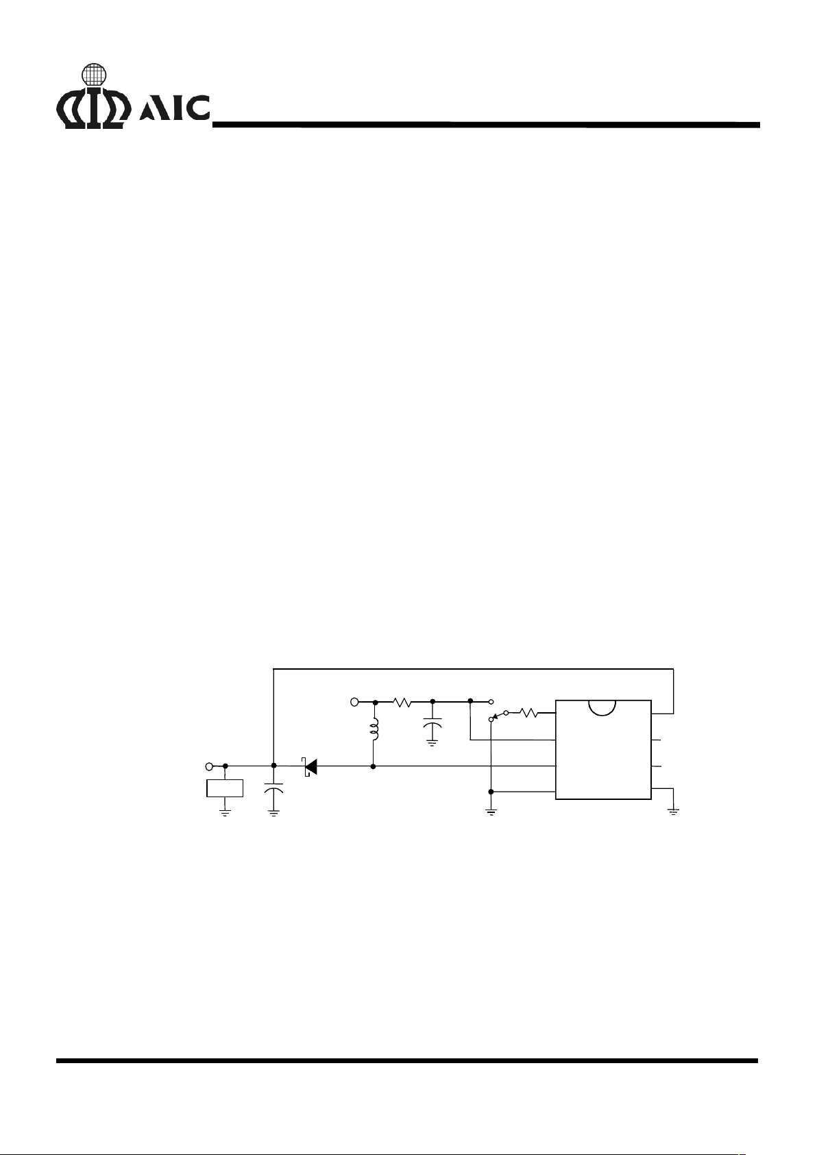
TYPICAL APPLICATION CIRCUIT
AIC1631
LOAD
100µF
NORMAL
R
ILIM
SD
ILIM/SD VOUT
VIN LBI
SW LBO
SGND CGND
+V
IN
1N5819
D1
+
+
C1
R1
L
C2
100µF
50µH
100Ω
+V
OUT
(3.3V)
Note: VIN≥≥≥≥1.8V, V
OUT
≤≤≤≤7V
High Efficiency Step-Up DC/DC Converter
AIC1631
2
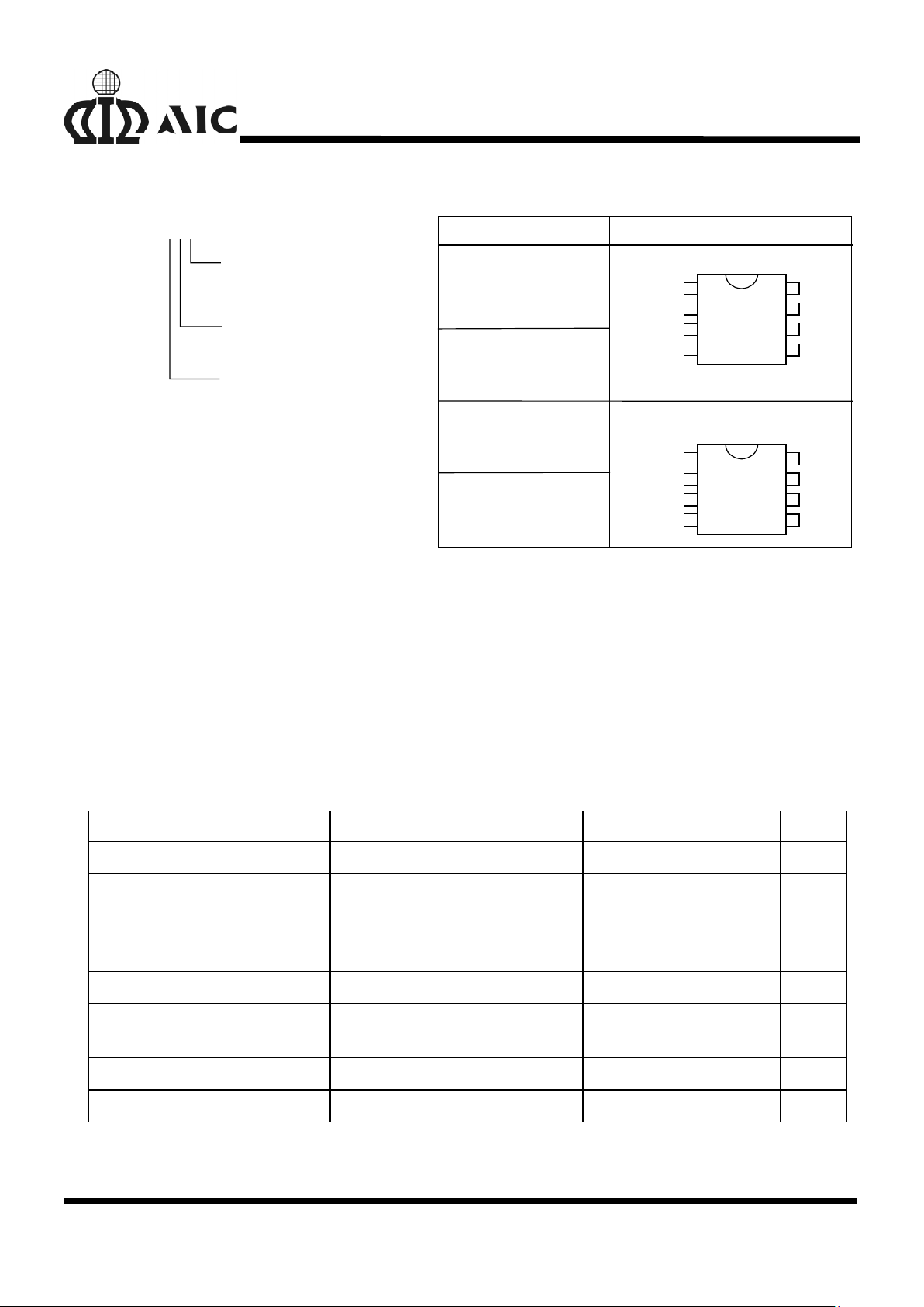
ORDERING INFORMATION
PACKAGE TYPE
N: PLASTIC DIP
S: SMALL OUTLINE
TEMPERATURE RANGE
C=0°C~+70°C
OUTPUT VOLTAGE
DEFAULT:3.3V
3: 3.0V
5: 5.0V
A: Adjustable
ORDER NUMBER
AIC1631CN
AIC1631-3CN
AIC1631-5CN
(PLASTIC DIP
)
PIN CONFIGURATION
AIC1631CS
AIC1631-3CS
AIC1631-5CS
(PLASTIC SO)
TOP VIEW
LBO
1
3
4
2
8
6
5
7
VOUT
VIN
SW
SGND
LBI
CGND
ILIM/SD
AIC1631ACN
(PLASTIC DIP
)
AIC1631ACS
(PLASTIC SO)
TOP VIEW
LBO
1
3
4
2
8
6
5
7
VOUT
VIN
EXT
GND
LBI
FB
ILIM/SD
AIC1631 XXX
ABSOLUTE MAXIMUM RATINGS
Supply Voltage ......................................…………....................…………....................... 7.0V
Operating Temperature Range.....................……..............………................... -20
°C ~ 80°C
Storage Temperature Range .......................………...................……….......
-65°C ~ 150°C
TEST CIRCUIT
Refer to Typical Application Circuit.
ELECTRICAL CHARACTERISTICS
(VIN=3.0V, Ta=25°°°°C, unless otherwise specified.)
PARAMETER TEST CONDITIONS MIN. TYP. MAX. UNIT
Input Voltage Fig. 4 in Appl. Examples 1.5 7 V
Output Voltage I
LOAD
=200mA
AIC1631
AIC1631-3
AIC1631-5
3.16
2.88
4.80
3.3
3
5
3.44
3.12
5.20
V
Switch off Current 105 140 µA
No Load Current AIC1631/AIC1631-3
AIC1631-5
160
180
µA
Shutdown Mode Current 7 15 µA
Shutdown Recovery Time VIN=2.5V, I
LOAD
=200mA 0.4 mS
AIC1631
3
ELECTRICAL CHARACTERISTICS
(CONTINUED)
PARAMETER TEST CONDITIONS MIN. TYP. MAX. UNIT
Efficiency I
LOAD
=200mA
AIC1631/AIC1631-3
AIC1631-5
87
90
%
Line Regulation I
LOAD
=100mA
AIC1631, V
IN
=1.8 ~ 3.3V
AIC1631-3, V
IN
=1.8 ~ 3V
AIC1631-5, V
IN
=2.2 ~ 3.3V
0.6
0.5
0.8
%V
OUT
Load Regulation I
LOAD
=10~300mA
AIC1631/AIC1631-3
AIC1631-5
0.3
0.8
%V
OUT
Oscillator Frequency 90 120 150 KHz
LBI Pin Trip Point 1.17 1.22 1.27 V
FB Threshold Voltage AIC1631A 0.598 0.617 0.636 V
SW “ON Resistance” AIC1631/AIC1631-3
AIC1631-5
0.5
0.4
Ω
LBO “ON Resistance” VIN=2V 45 Ω
SW Off Leakage 1 µA
Input Pin Bias Current 10 nA/Pin
Output Pin Leakage 10 nA/Pin
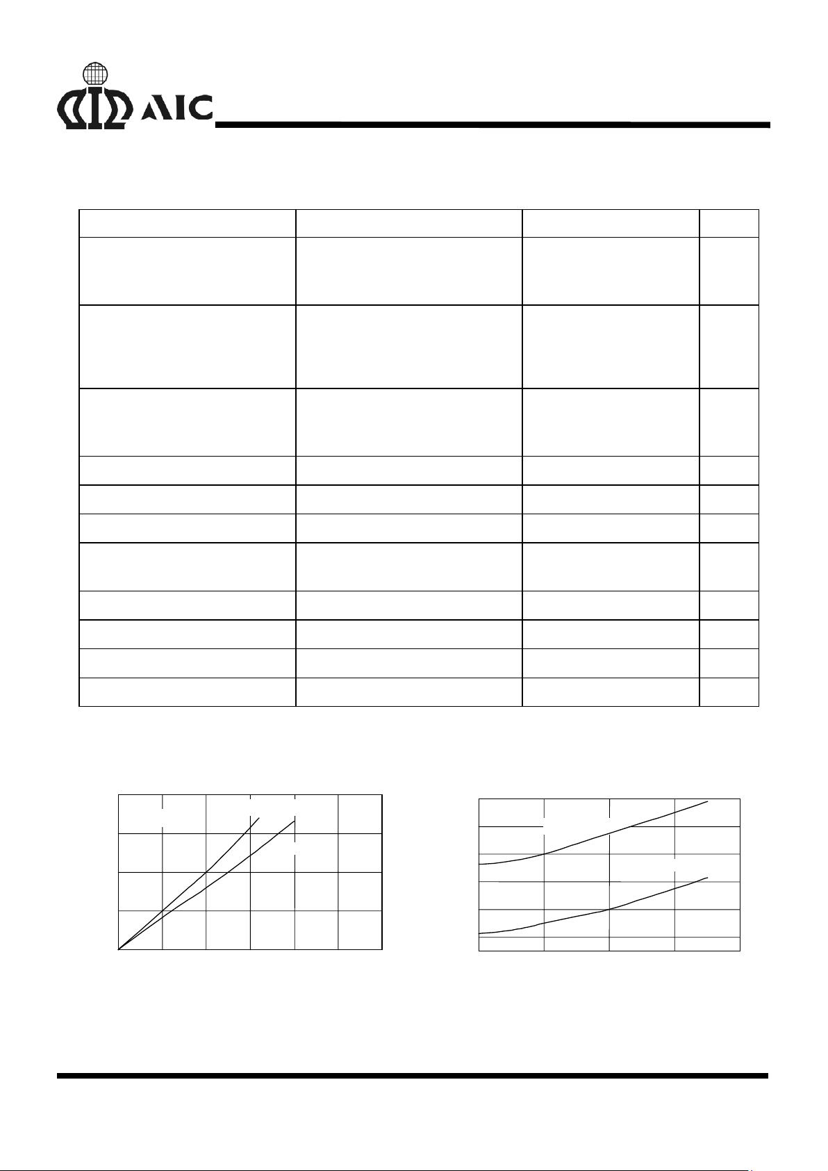
TYPICAL PERFORMANCE CHARACTERISTICS
ISW (A)
1
0 0.5 1 1.5 2 2.5 3
0
0.25
0.5
0.75
Ta=25°C
A
IC1631/1631-3
A
IC1631-5
V
SW
(V)
Switch Voltage vs. Current
020406080
0.36
0.38
0.42
0.46
0.5
.0.54
0.58
Temperature (°C)
A
IC1631/1631-3
A
IC1631-5
SW R
DS
(
Ω
)
SW ON Resistance vs. Temperature
 Loading...