

AIC AIC1573 Datasheet

AIC1573
5-bit DAC, Synchronous PWM Power
Regulator with Simple PWM Power Regulator,
LDO And Linear Controller
Analog Integrations Corporation 4F, 9, Industry E. 9th Rd, Science Based Industrial Park, Hsinchu Taiwan, ROC
www.analog.com.tw
DS-1573-01 Sep 10, 01 TEL: 886-3-5772500 FAX: 886-3-5772510 1
n
FEATURES
l Compatible with HIP6020.
l Provides 4 Regulated Voltages for Microprocessor
Core, AGP Bus, Memory and GTL Bus Power.
l TTL Compatible 5-bit Digital-to-Analog Core Output
Voltage Selection. Range from 1.3V to 3.5V.
0.1V Steps from 2.1V to 3.5V.
0.05V Steps from 1.3V to 2.05V.
l ±1.0% PWM Output Voltage for VCORE .
l ±3% PWM Output Voltage for AGP Bus.
l ±3.0% Reference Voltage for Chipset and/or Ca-
che Memory and VGTL.
l Simple Voltage-Mode PWM Control with Built in
Internal Compensation Network s.
l N-Channel MOSFET Driver for PWM buck con-
verters.
l Linear Controller Drives Compatible with both N–
Chanel MOSFET and NPN Bipolar Series Pass
Transistor.
l Operates from +3.3V, +5V and +12V Inputs.
l Fast Transient Response.
l Full 0% to 100% Duty Ratios.
l Adjustable Current Limit without External Sense
Resistor.
l Microprocessor Core Voltage Protection against
Upper MOSFET shorted to +5V .
l Power Good Output Voltage Monitor.
l Over-Voltage and Over-Current Fault Monitors.
l 200KHz Free-Running Oscillator Programmable up
to 700KHz.
n
APPLICATIONS
l Full Motherboard Power Regulation for Computers.
n
DESCRIPTION
The AIC1573 combines two PWM voltage mode
controllers and two linear controllers as well as the
monitoring and protection functions in this chip. One
PWM controller regulates the microprocessor core
voltage with a synchronous rectified buck converter.
The second PWM controller provides AGP bus 1.5V
or 3.3V power with a standard buck converter. Two
linear controllers regulate power for the 1.5V GTL
bus and 1.8V power for the chip set core voltage
and/or cache memory circuits.
An integrated 5 bit D/A converter that adjusts the
microprocessor core voltage from 2.1V to 3.5V in
0.1V increments and from 1.3V to 2.05V in 0.05V
increments. The second PWM controller for AGP
bus power is selectable by means of SELECT pin
status for 1.5V or 3.3V with 3% accuracy. Two linear
controllers drive with external N-channel MOSFETs
to provide 1.5V±3% and fixed output voltage
1.8V±3%.
This chip monitors all the output voltages. Power
Good signal is issued when the core voltage is
within ±10% of the DAC setting and the other levels
are above their under-voltage levels. Over-voltage
protection for the core output uses the lower Nchannel MOSFET to prevent output voltage above
116% of the DAC setting.
The PWM over-current function monitors the output
current by using the voltage drop across the upper
MOSFET’s R
DS(ON)
, eliminating the need for a cur-
rent sensing resistor.
AIC1573
2
n
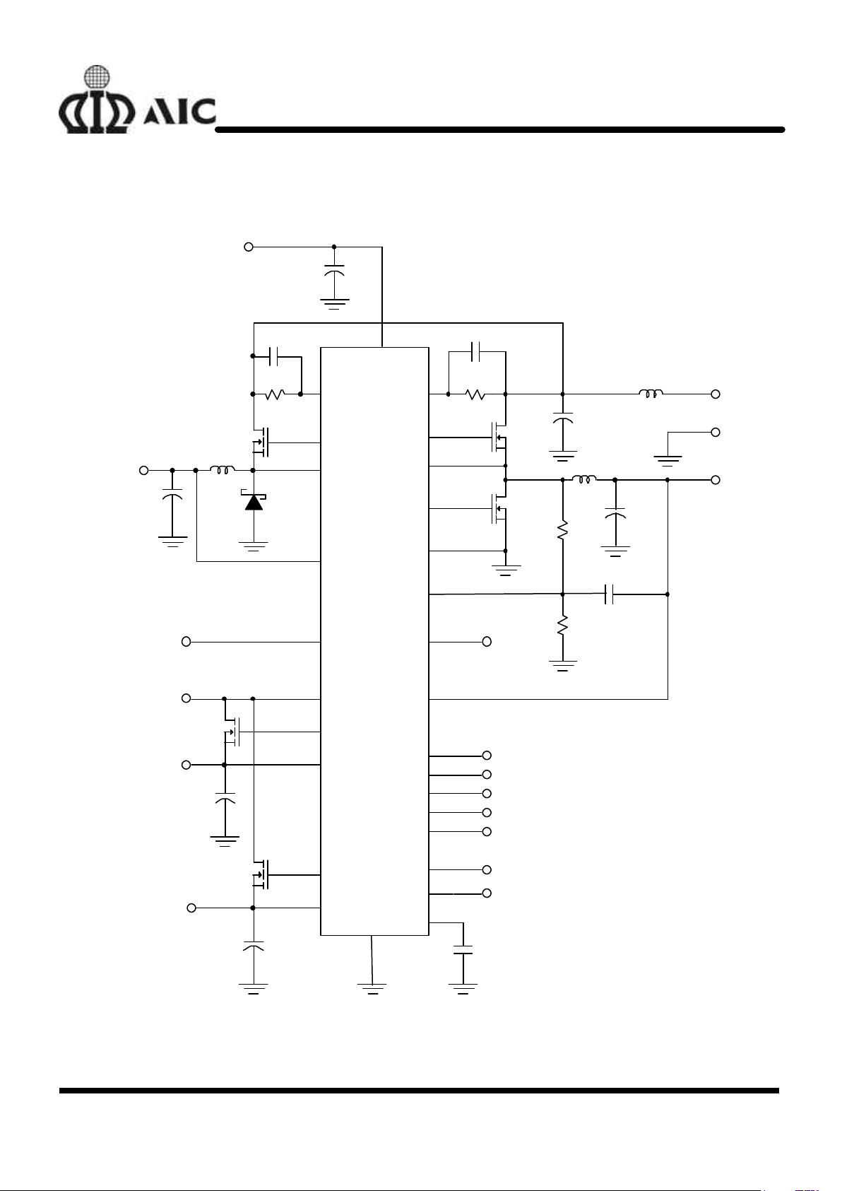
APPLICATION CIRCUIT
+
+
+
+
+
+
UGATE1
UGATE2
PHASE1
PHASE2
LGATE1
PGND
VSEN2
FB1
SELECT
NC
VAUX
VSEN1
DRIVE3
VID0
VSEN3
VID1
VID2
VID3
VID4
PGOOD
DRIVE4
FAULT/RT
VESN4
SS
7µH
3µH
4.7µF
8
13
7
6
5
4
3
1nF
1nF
C7
C5
1000µF*3
1000µF*7
20
0.22µF
C6
680K
10K
R2
R1
10V
680µF*7
C
IN
R3
L1
V
OUT1
21
L3
22
C
OUT1
OCSET1
23
24
25
26
27
GND
+5V
IN
1µH
Q2
Q1
9
3.3V or 1.5V
V
OUT2
Q5
Q4
Q3
C
OUT3
C
OUT4
C
OUT2
14
CssGND
1.8V
V
OUT4
15
11
16
V
OUT3
19
18
1.5V
+3.3V
IN
28
1
+12V
IN
OCSET2
L2
10
2
VCC
17
12
AIC1573
3
n
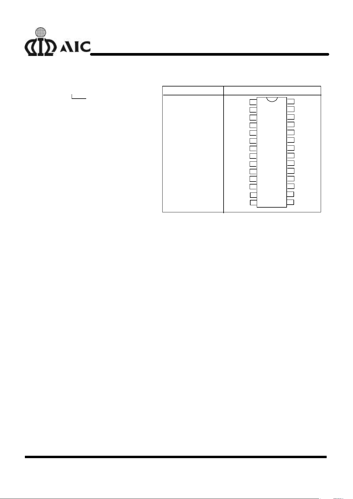
ORDERING INFORMATION
ORDER NUMBER
PIN CONFIGURATION
AIC1573 -CX
AIC157 3CS
(SO28 )
PACKAGING TYPE
S: SMALL OUTLINE
1342576
8910
VID
1
PHASE2
VID4VID3UGATE2
VID
2
VSEN2
VID0
OCSET2
PGOOD
1112SS
SELECT
PHASE1
VCC
UGATE1
OCSET1
LGATE1
PGND2019VSEN1
VSEN3FB1NC28262725
242321221817GND
DRIVE3
13
1
4
VSEN4
FAULT/RT
1615
DRIVE4
VAUX
n
ABSOLUTE MAXIMUM RATINGS
Supply Voltage, VCC ...............…………….....………….........…..……..................... +15V
PGOOD, FAULT and GATE Voltage .....……….....………..….... GND -0.3V to VCC +0.3V
Input, Output , or I/O Voltage ......…...………………………..……............ GND -0.3V to 7V
Recommended Operating Conditions
Supply Voltage; VCC……..…………...........…................... +12V±10%
Ambient Temperature Range ……..……..………................. 0°C~70°C
Junction Temperature Range ……....… .……….................. 0°C~125°C
Thermal Information
Thermal Resistance, θ
JA
SOIC package …………………………………..… ..… .............. 70°C/W
SOIC package (with 3in2 of copper) …...… ..…….......…......... 50°C/W
Maximum Junction Temperature (Plastic Package) …………………..……...... 150°C
Maximum Storage Temperature Range ……………………..……….... -65°C ~ 150°C
Maximum Lead Temperature (Soldering 10 sec) …………………………..…... 300°C
AIC1573
4
n
ELECTRICAL CHARACTERISTICS
(Vcc=12V, TA=25°C, Unless otherwise specified)
PARAMETER TEST CONDITIONS SYMBOL MIN. TYP. MAX. UNIT
VCC SUPPLY CURRENT
Supply Current UGATE1, LGATE1, UGATE2,
DRIVE3 and DRIVE4 open
I
CC
3 mA
POWER ON RESET
Rising VCC Threshold VOCSET=4.5V
V
CCTHR
10.4 V
Falling VCC Threshold VOCSET=4.5V
V
CCTHF
8.2 V
Rising VAUX Threshold
VAUX
THR
2.5 V
VAUX Threshold Hy steresis
VAUX
HYS
500 mV
Rising VOCSET1 Threshold
V
OCSETH
1.26 V
OSCILLATOR
Free Running Frequency RT=Open F 170 200 230 KHz
Total Variation 6kΩ<RT to GND<200k Ω -15 +15 %
Ramp. Amplitude RT=open
∆V
OSC
1.5 VP-P
DAC AND STANDARD BUCK REGULATOR REFERENCE
DAC (VID0~VID4) Input Low
Voltage
V
IDL
0.8 V
DAC (VID0~VID4) Input High
Voltage
V
IDH
2.0 V
DACOUT Voltage Accuracy
V
DAC
=1.8V~3.5V
-1.0 +1.0 %
PWM2 Reference Voltage Select < 0.8V
1.5 V
PWM2 Reference Voltage Select > 2.0V
3.3 V
PWM2 Reference Voltage
Tolerance
3 %
1.5V AND 1.8V LINEAR REGULATORS ( OUT3, OUT4)
Regulation
3 %
VSEN3 Regulation Voltage
V
REG3
1.5 V
VSEN4 Regulation Voltage
V
REG4
1.8 V
Under-Voltage Level
( V
SEN/VREG
)
V
SEN
Rising
V
SENUV
75 %
Under-Voltage Hysteresis
(V
SEN/VREG
)
V
SEN
Falling
5 %
Output Drive Current ( All
Linears )
V
AUX-VDRIVE
> 0.6V
20 30 mA
AIC1573
5
n
ELECTRICAL CHARACTERISTICS
(Continued)
PARAMETER TEST CONDITIONS SYMBOL MIN. TYP. MAX. UNIT
SYNCHRONOUS PWM CONTROLLER AMPLIFIER
DC Gain
(G.B.D.)
80 dB
Gain-Bandwidth Product
(G.B.D.)
G
BWP
13 MHz
Slew Rate
(G.B.D.) note 1.
S
R
6 V/µs
PWM CONTROLLER GATE DRIVERS
U
GATE1,2
Upper Drive Source
VCC=12V, V
UGATE
= 6V I
UGH
0.9 A
U
GATE1,2
Upper Drive Sink
V
UGATE
=1V R
UGL
2.8 3.5 Ω
Lower Drive Source
VCC=12V, V
LGATE
=1V I
LGH
1 A
Lower Drive Sink
V
LGATE
=1V R
LGL
2.2 3.0 Ω
PROTECTION
VSEN1 Over-Voltage
( V
SEN1
/DACOUT)
V
SEN1
Rising OVP 116 120 %
FAULT Sourcing Current
V
CC-VFAULT/RT
=2.0V
I
OVP
20 mA
OCSET1,2 Current Source
V
OCSET
=4.5VDC
I
OCSET
170 200 230 µA
Soft-Start Current
I
SS
25 µA
POWER GOOD
V
SEN1
Upper Threshold
( V
SEN1
/DACOUT )
V
SEN1
Rising 108 111 %
V
SEN1
Under-Voltage
( VSEN1/DACOUT )
V
SEN1
Falling 92 95 %
V
SEN1
Hysteresis
(VSEN1/DACOUT)
Upper and Lower Threshold
2 %
P
GOOD
Voltage Low
I
PGOOD
=-4mA V
PGOOD
0.4 0.8 V
Note 1. Without internal compensation network, the gain bandwidth product is 13MHz. Being associated with
internal compensation networks, the Bode Plot is shown in Fig. 3, “Internal Compensation Gain of
PWM Error Amplifier”.
AIC1573
6
n
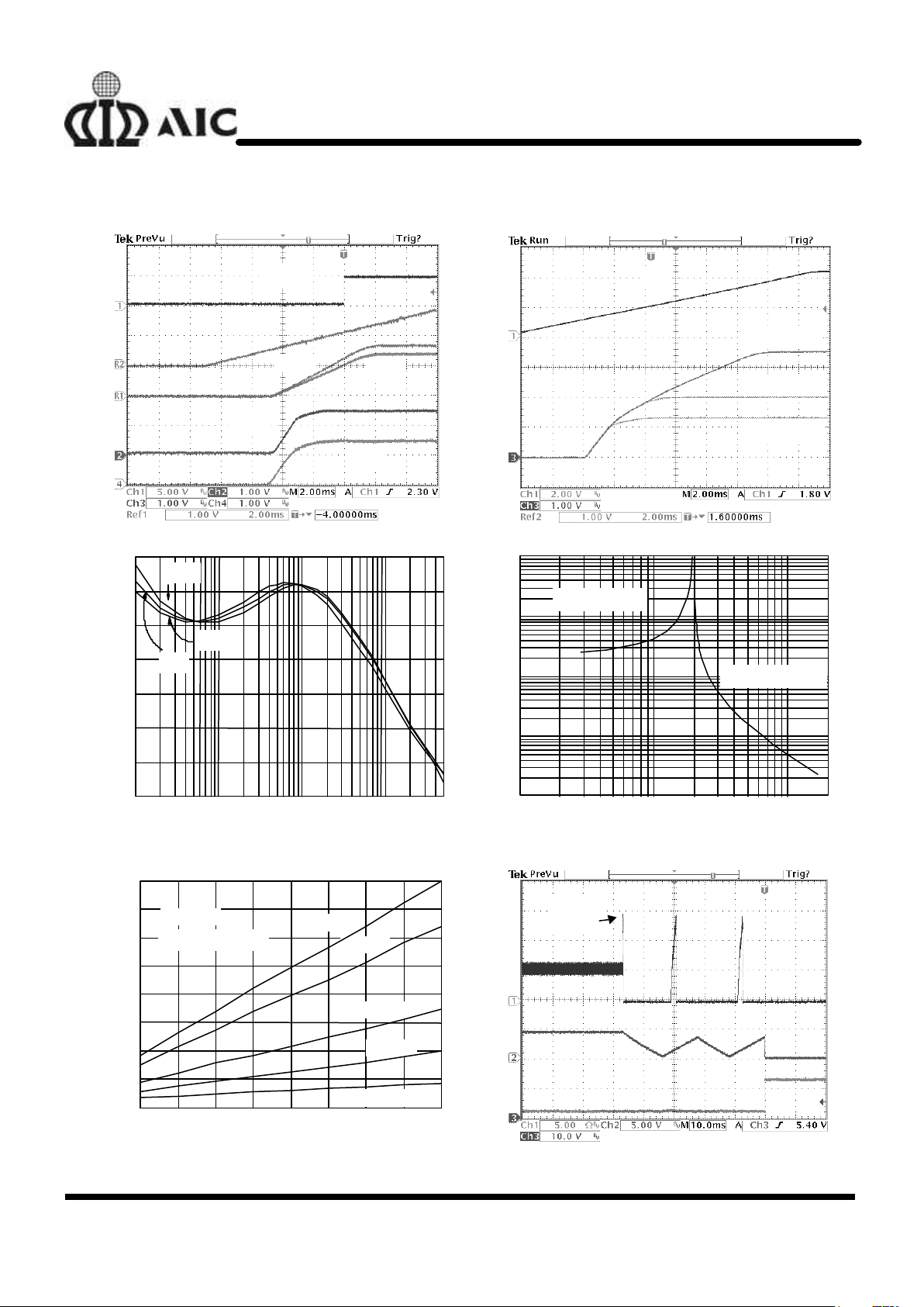
TYPICAL PERFORMANCE CHARACTERISTICS
Fig. 1 Soft Start Interval with 4 Outputs and P
GOOD
PGOOD
SS
V
OUT3
V
OUT2
V
OUT1
V
OUT4
SS
VDAC=3.5V
VDAC=2V
VDAC=1.3V
Fig. 2 Soft Start Initiates PWM Output
1k 10k 100k 1M
-5
0
5
10
15
20
25
30
90°C
Gain (dB)
Frequency (Hz)
Fig 3. Internal Compensation Gain of PWM Error Amplifier
-40°C
22°C
10k 100k 1M
1k
10k
100k
1M
10M
R
T
Pull Up to 12V
Resistance (Ω)
Switching Frequency (Hz)
R
T
Pull Down to GND
Fig. 4
RT Resistance vs. Frequency
Switching Frequency (Hz)
200k
400k
500k
600k
700k
900k0204060
80
100
120
140
160
I
CC
(mA)
VCC=12V
C
UG1=CLG1=CUG2
=C
C=4.7nF
C=3.3nF
C=1.5nF
C=650pF
C=0
Fig. 5 Supply Current vs. Frequency
SS
Inductor
Current 5A/div
Over Load
Applied
Fault
Fig. 6 Over Current ON Inductor
 Loading...