

AIC AIC1571 Datasheet

AIC1571
5-bit DAC, Synchronous PWM Power
Regulator with Dual Linear Controllers
Analog Integrations Corporation 4F, 9, Industry E. 9th Rd, Science Based Industrial Park, Hsinchu Taiwan, ROC www.analog.com.tw
DS-1571-00 Oct 9, 00 TEL: 886-3-5772500 FAX: 886-3-5772510
1
FEATURES
Provides 3 Regulated Voltages for Microprocessor Core, Clock and GTL Power.
Simple Voltage-Mode PWM Control.
Dual N-Channel MOSFET Synchronous Driver.
Operates from +3.3V, +5V and +12V Inputs.
Fast Transient Response.
Full 0% to 100% Duty Ratios.
±1.0% Output Voltage for VCORE and ±2.0%
Output Voltage Reference for VCLK and VGTL.
TTL Compatible 5-bit Digital-to-Analog Core Output Voltage Selection. Range from 1.3V to 3.5V.
0.1V Steps from 2.1V to 3.5V.
0.05V Steps from 1.3V to 2.05V.
Adjustable Current Limit without External Sense
Resistor.
Microprocessor Core Voltage Protection against
Shorted MOSFET.
Power Good Output Voltage Monitor.
Over-Voltage and Over-Current Fault Monitors.
200KHz Free-Running Oscillator Programmable
up to 350KHz.
APPLICATIONS
Full Motherboard Power Regulation for Computers.
Power Integrations for 3 Output Power System.
DESCRIPTION
The AIC1571 combines a synchronous voltage
mode controller with two linear controllers as well
as the monitoring and protection functions in this
chip. The PWM controller regulates the microproc-
essor core voltage with a synchronous rectified
buck converter. One linear controller regulates
power for the GTL bus and the other linear con-
troller provides power for the clock driver circuit or
memory (1.8V)
An integrated 5 bit D/A converter that adjusts the
core PWM output voltage from 2.1V to 3.5V in 0.1V
increments and from 1.3V to 2.05V in 0.05V incre-
ments. The linear regulator uses an internal driver
device to provide 2.5V±2.5%. The linear controller
drives with an external N-channel MOSEFET to
provide 1.5V±2.5%.
This chip monitors all the output voltages. Power
Good signal is issued when the core voltage is
within ±10% of the DAC setting and the other levels
are above their under-voltage levels. Over-voltage
protection for the core output uses the lower N-
channel MOSFET to prevent output voltage above
115% of the DAC setting.
The PWM over-current function monitors the out-
put current by using the voltage drop across the
upper MOSFET’s R
DS(on)
, eliminating the need for a
current sensing resistor
.
AIC1571
2
ORDERING INFORMATION
ORDER NUMBER
PIN CONFIGURATION
AIC1571-CX
AIC1571CS
(SO24)
PACKAGING TYPE
S: SMALL OUTLINE
1
3
4
2
5
7
6
8
9
10
VID0
VID4
VID3
VID2
VCC
VID1
RT
PGOOD
SS
FAULT
LGATE
UGATE
PHASE
VSEN
PGND
OCSET
16
15
FB1
GATE3
COMP1
FB3
24
22
23
21
20
19
17
18
11
12VIN2
FB2
14
13 GATE 2
GND
ABSOLUTE MAXIMUM RATINGS
Supply Voltage, VCC ...............…………….....………….........…..……..................... +15V
PGOOD, FAULT and GATE Voltage .....…….....………..….... GND -0.3V to V
CC
+0.3V
Input, Output , or I/O Voltage ......…...……………………..……............ GND -0.3V to 7V
Recommended Operating Conditions
Supply Voltage; VCC ……...............…................... +12V±10%
Ambient temperature Range ……..……………................. 0°C~70°C
Junction Temperature Range ……......……….................. 0°C~100°C
Thermal Information
Thermal Resistance, θ
JA
SOIC package …………………………………..…............... 100°C/W
SOIC package (with 3in
2
of copper) …...……….......…......... 90°C/W
Maximum Junction Temperature (Plastic Package) ………………..……...... 150°C
Maximum Storage Temperature Range …………………………….... -65°C ~ 150°C
Maximum Lead Temperature (Soldering 10 sec) ………………………..…... 300°C
TEST CIRCUIT
Refer to APPLICATION CIRCUIT.
AIC1571
3
ELECTRICAL CHARACTERISTICS
(Vcc=12V, TJ=25°°°°C, Unless otherwise speci-
fied)
PARAMETER TEST CONDITIONS
SYMBOL
MIN. TYP. MAX. UNIT
VCC SUPPLY CURRENT
Supply Current UGATE, LGATE, GATE2
and GATE3 open
I
CC
1.8 5 mA
POWER ON RESET
Rising VCC Threshold V
OCSET
=4.5V VCC
THR
8.6 9.5 10.4 V
Falling VCC Threshold V
OCSET
=4.5V VCC
THF
8.2 9.2 10.2 V
Rising VIN2 Under-Voltage
Threshold
VIN2
THR
2.5 2.6 2.7 V
VIN2 Under-Voltage Hysteresis
VIN2
HYS
130 mV
Rising V
OCSET1
Threshold V
OCSETH
1.3 V
OSCILLATOR
Free Running Frequency RT=Open F 170 200 230 KHz
Ramp. Amplitude RT=open ∆V
OSC
1.3 V
P-P
REFERENCE AND DAC
DAC (VID0~VID4) Input Low
Voltage
VID
L
0.8 V
DAC (VID0~VID4) Input
High Voltage
VID
H
2
V
DACOUT Voltage Accuracy VDAC=1.3V~3.5V -1.0 +1.0 %
FB2 Reference Voltage V
REF2
1.245 1.270 1.295 V
FB3 Reference Voltage V
REF3
1.250 1.275 1.300 V
AIC1571
4
ELECTRICAL CHARACTERISTICS
(Continued)
PARAMETER TEST CONDITIONS
SYMBOL
MIN. TYP. MAX. UNIT
LINEAR CONTROLLER
Regulation 0 < I
GATE2/3
< 10mA -2.5 +2.5 %
Under-Voltage Level FB2/3 falling FB2/3
UV
70 80 %
PWM CONTROLLER ERROR AMPLIFIER
DC GAIN 76 dB
Gain Bandwidth Product GBWP 11 MHz
Slew Rate COMP1=10pF SR 6 V/µS
PWM CONTROLLER GATE DRIVER
Upper Drive Source VCC=12V, V
UGATE
=11V R
UGH
5.2 6.5 Ω
Upper Drive Sink VCC=12V, V
UGATE
=1V R
UGL
3.3 5 Ω
Lower Drive Source VCC=12V, V
LGATE
=11V R
LGH
4.1 6 Ω
Lower Drive Sink VCC=12V, V
LGATE
=1V R
LGL
35Ω
PROTECTION
V
OUT1
Voltage Over-Voltage
Trip
VSEN Rising OVP 112 115 118 %
OCSET Current Source V
OCSET
=4.5V
DC
I
OCSET
170 200 230 µA
FAULT Sourcing Current V
FAULT
=10V I
OVP
10 16 mA
Soft-Start Current I
SS
11 µA
Chip Shutdown Soft Start
Threshold
1.0 V
POWER GOOD
V
OUT1
Upper Threshold VSEN Rising 109 110.5 112 %
V
OUT1
Under-Voltage VSEN Falling 90.5 92 93.5 %
V
OUT1
Hysteresis
(VSEN/DACOUT)
Upper and Lower Threshold
3%
P
GOOD
Voltage Low I
PGOOD
=-4mA V
PGOOD
0.5 V
AIC1571
5
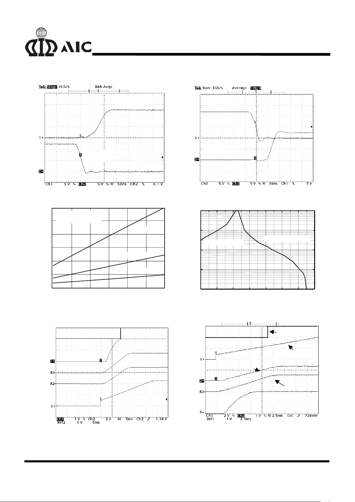
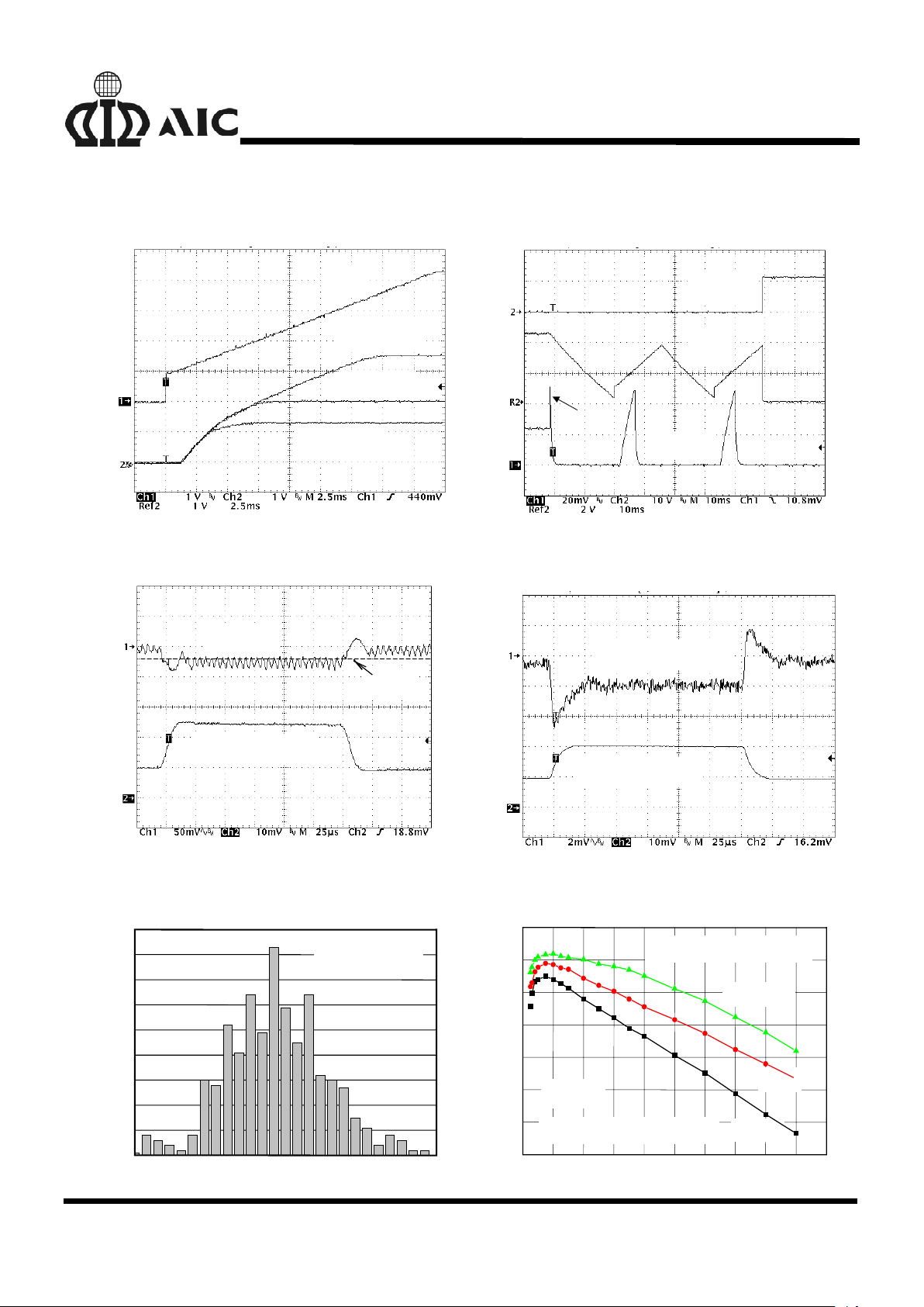
TYPICAL PERFORMANCE CHARACTERISTICS
U
GATE
L
GATE
U
GATE
L
GATE
FIG.1 The gate drive waveforms
I
CC
(mA)
Switching Frequency (KHz)
100 150 200 25 0 30 0 350 400
0
10
20
30
40
50
60
C
UGATE=CLGATE=CGATE
VCC=12V
C
GATE
=5000pF
C
GATE
=2000pF
C
GATE
=660pF
100 150
200
250
300
350 400
1
10
100
1000
10000
Resistance (k
Ω
)
Switching Frequency (KHz)
R
Pull Down to GND
RT Pull Up to +12V
450
FIG. 2 Bias Supply Current VS. Frequency FIG. 3 RT Resistance VS. Frequency
V
OUT2
(1V/div)
SS (2V/div)
V
OUT3
(1V/div)
V
OUT1
(1V/div)
PGOOD (5V/div)
SS (2V/div)
V
OUT1
(1V/div)
V
OUT3
SS (2V/div)
PGOOD (5V/div)
V
OUT1
(1V/div)
SS (2V/div)
V
OUT3
V
OUT2
(1V/div)
PGOOD (5V/div)
FIG.4-1 Circuit 1---Soft Start Interval with 3 Outputs FIG.4-2 Circuit 2---Soft Start Interval with 3
and PGOOD Outputs and PGOOD
AIC1571
6
TYPICAL PERFORMANCE CHARACTERISTICS
(CONTINUED)
VDAC=3.5V
VDAC=1.3V
VDAC=2V
SS
FAULT
SS
10A/div
Inductor Current
Over Load
A
pplied
FIG. 5 Soft Start Initiates PWM Output FIG. 6 Over-Current Operation on Inductor
V
OUT1
5A to 12A Load Step
2.0V
DC
V
OUT3
(
2mV/di v
)
1A to 2A Load Step
FIG. 7 Transient Response of PWM Output FIG. 8 Transient Response of Linear Controller
-0.5 -0.4 -0.3 -0.2 -0.1 0.0 0.1 0.2 0.3 0.4 0.5 0.6 0.70
10
20
30
40
50
60
70
80
90
N
um
b
er o
f
P
ar
t
s
DACOUT=2.0V
TA= 25°C
0 2 4 6 8 10 12 14 16 18 20
65
70
75
80
85
90
95
100
Power MOSFET : CEB6030L
Vo=2.8 V
Vo=2V
Vo=1.3 V
VIN=5V
Switching Frequency = 200KHz
Efficiency (%)
FIG. 9 DACOUT Voltage Accuracy (%) FIG.10 Efficiency vs. Load Current (A)
 Loading...