

AIC AIC1569A Datasheet

AIC1569A
5-bit DAC, Synchronous PWM Power Regulator
FEATURES
Compatible with HIP6004.
Simple Voltage-Mode PWM Control.
Dual N-Channel MOSFET Synchronous Drive.
Fast Transient Response.
±1% 5-Bit Digital-to-Analog Output Voltage.
Adjustable Current Limit Without External
Sense Resistor.
Full 0% to 100% Duty Ratio.
200KHz Free-Running Oscillator,
Programmable up to 350KHz.
Power-Good Output Voltage Monitor.
APPLICATIONS
Power Supply for Pentium® II, Power® and
Alpha® Microprocessors.
High-Power 5V to 3.xV DC/DC Regulators.
Low-Voltage Distributed Power Supplies.
DESCRIPTION
The AIC1569A is a high power, high efficiency
switching regulator controller optimized for high
performance microprocessor applications. It is
designed to drive dual N-channel MOSFETs in a
standard synchronous buck topology. Featuring
a digitally programmable switching regulator, the
AIC1569A includes monitoring and protection
capabilities in addition to all the essential
synchronous PWM control functions.
The internal 5-bit Digital-to-Analog Converter
(DAC) adjusts the output voltage from 2.0V to
3.5V in 0.1V increments and 1.3V to 2.0V in
0.05V increments. The precision reference and
voltage-mode control can provide output
regulation within ±1% over temperature and line
voltage shifts.
The internal oscillator of the AIC1569A free-runs
at 200KHz and can be adjusted up to 350KHz.
The resulting PWM duty ratio ranges from 0% to
100%. The error amplifier features an 11MHz
bandwidth and 6V/µS slew rate, which enables
high converter bandwidth for fast transient
response.
The AIC1569A provides adjustable over current
and short circuit protections. It senses the output
current across the on resistance of the upper N-
channel MOSFET without an external low value
sense resistor. It also monitors the output voltage
with a window comparator and issues a power
good signal when the output is within 10% of the
rated output voltage.
Analog Integrations Corporation 4F, 9, Industry E. 9th Rd, Science Based Industrial Park, Hsinchu Taiwan, ROC www.analog.com.tw
DS-1569A-00 TEL: 886-3-5772500 FAX: 886-3-5772510
1
ORDERING INFORMATION
AIC1569A
AIC1569A XX
PACKAGE TYPE
S: SMALL OUTLINE
TEMPERATURE RANGE
C: 0°C~70°C
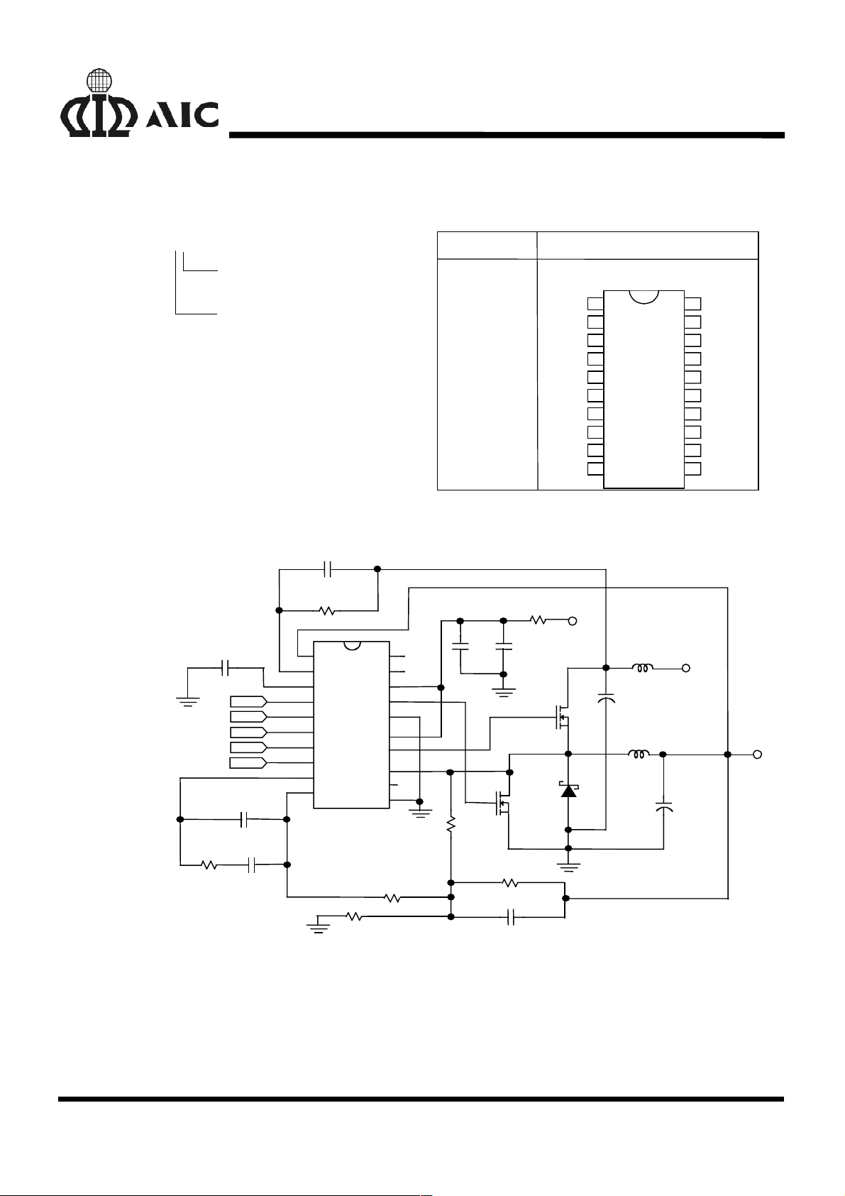
TYPICAL APPLICATION CIRCUIT
C9
1000pF
R2
2.2K
C8
0.1µF
VID0
VID1
VID2
VID3
VID4
C7
33pF
C6
R6
90.9K
1000pF
VSEN
OCSET
SS
VID0
VID1
VID2
VID3
VID4
COMP
FB
AIC1569A
R7
1.2M
RT
OVP
VCC
LGATE
PGND
BOOT
UGATE
PHASE
PGOOD
GND
R5
3.01K
DC/DC Converter for Pentium
ORDER NUMBER
AIC1569ACS
(PLASTIC SO)
0.1µF
0.1µF
R3
47K
C5
II V
C1
1µF
M2
NDP603AL
R4
15K
C2
R1
47Ω
CORE
PIN CONFIGURATION
TOP VIEW
1
VSEN
2
OCSET
3
SS
4
VID0
VID1
5
6
VID2
7
VID3
8
VID4
9
COMP
10
FB
12V
M1
D1
+
RFP45N03L
1N5820
L1
1µH
C3
1000µF x 3
L2
3µH
+
20
RT
19
OVP
VCC
18
LGATE
17
PGND
16
15
BOOT
14
UGATE
13
PHASE
12
PGOOD
11
GND
5V
C4
1000µF x 8
VOUT
2
ABSOLUTE MAXIMUM RATINGS
Supply Voltage, VCC....…...........................….……....………….......................................... 15V
Boot Voltage, V
Input, Output, or I/O Voltage .....................…………...…...……....... GND - 0.3V to VCC+0.3V
ESD Classification ..............................……………….…................……......................... Class 2
Recommended Operating Conditions
Supply Voltage, V
Ambient Temperature Range .…............................…....…………….….................. 0°C ~ 70°C
Junction Temperature Range ....…...........……………..........…............................. 0°C ~100°C
Thermal Information
Thermal Resistance, θ
SOIC Package...............................………….……..…………………….........…. 100°C /W
SOIC Package (with 3 in
Maximum Junction Temperature (Plastic Package) …..……………….....…….............. 150°C
Maximum Storage Temperature Range …………………………...........…......... -65°C ~150°C
Maximum Lead Temperature (Soldering 10 sec) ……….…………………......…......... 300°C
………........................………..…………............................................. 15V
BOOT
....…............................…………..……...................................... 12V±10%
CC
(Typical, Note 1)
JA
2
of Copper) ……………..………………………......….. 90°C /W
AIC1569A
Note 1:
θ
is measured with the component mounted on an evaluation PC board in free air.
JA
TEST CIRCUIT
Refer to TYPICAL APPLICATION CIRCUIT.
ELECTRICAL CHARACTERISTICS (VCC= 12V, Ta=25°
PARAM ETER TEST CONDITIONS SYMBOL MIN. TYP. MAX. UNIT
VCC Supply Current
Nominal Supply UGATE Open I
Power-On Reset
VCC Threshold V
Rising V
Oscillator
Free Running Frequency RT Open 170 200 230 KHz
Threshold 1.26 V
OCSET
=4.5V 8.2 9.3 10.2 V
OCSET
°C, unless otherwise specified.)
°°
VCC
1 3 mA
Total Variation 6KΩ<RT <200KΩ -20 +20 %
Ramp Amplitude RT Open ∆V
OSC
1.5 V
P-P
3
 Loading...