

AIC AIC1567CS, AIC1567 Datasheet

AIC1567
5-bit DAC, Synchronous PWM Power Regulator
with Linear Controller
Analog Integrations Corporation 4F, 9, Industry E. 9th Rd, Science Based Industrial Park, Hsinchu Taiwan, ROC www.analog.com.tw
DS-1567-00 TEL: 886-3-5772500 FAX: 886-3-5772510
1
FEATURES
Switching Regulator and Low Dropout Linear
Regulator on single chip.
Simple Voltage-Mode PWM Control.
Dual N-Channel MOSFET Synchronous Drive.
Fast Transient Response.
±1.0% 5-Bit Digital-to-Analog Output Voltage.
Adjustable Current Limit Without External Sense
Resistor.
Full 0% to 100% Duty Ratio.
200KHz Free-Running Oscillator Programmable
up to 350KHz.
Power-Good Output Voltage Monitor.
Short Circuit Protection with Low Short Circuit
Output Current.
APPLICATIONS
Power Supply for Pentium II, Power PC and
Alpha Microprocessors.
High-Power 5V to 3.xV DC/DC Regulators.
Low-Voltage Distributed Power Supplies.
DESCRIPTION
The AIC1567 is a high power, high efficiency
switching regulator controller optimized for high
performance microprocessor applications. It is
designed to drive dual N-channel MOSFET in a
standard synchronous buck topology.
Featuring a low dropout linear regulator and a
digitally programmable switching regulator, the
AIC1567 includes monitoring and protection
capabilities in addition to all the essential
synchronous PWM control functions.
The internal 5-bit Digital-to-Analog Converter
(DAC) adjusts the output voltage from 2.0V to
3.5V in 0.1V increments and 1.3V to 2.0V in
0.05V increments. The precision reference and
voltage-mode control can provide output
regulation within ±1.0% over temperature and
line voltage shifts.
The internal oscillator of the AIC1567 free-runs
at 200KHz and can be adjusted up to 350KHz.
The resulting PWM duty ratio ranges from 0% to
100%. The error amplifier features a 11MHz
bandwidth and 6V/µS slew rate, which enables
high converter bandwidth for fast transient
response.
AIC1567
2
ORDERING INFORMATION
AIC1567 XX
PACKAGE TYPE
S: SMALL OUTLINE
TEMPERATURE RANGE
C: 0°C~70°C
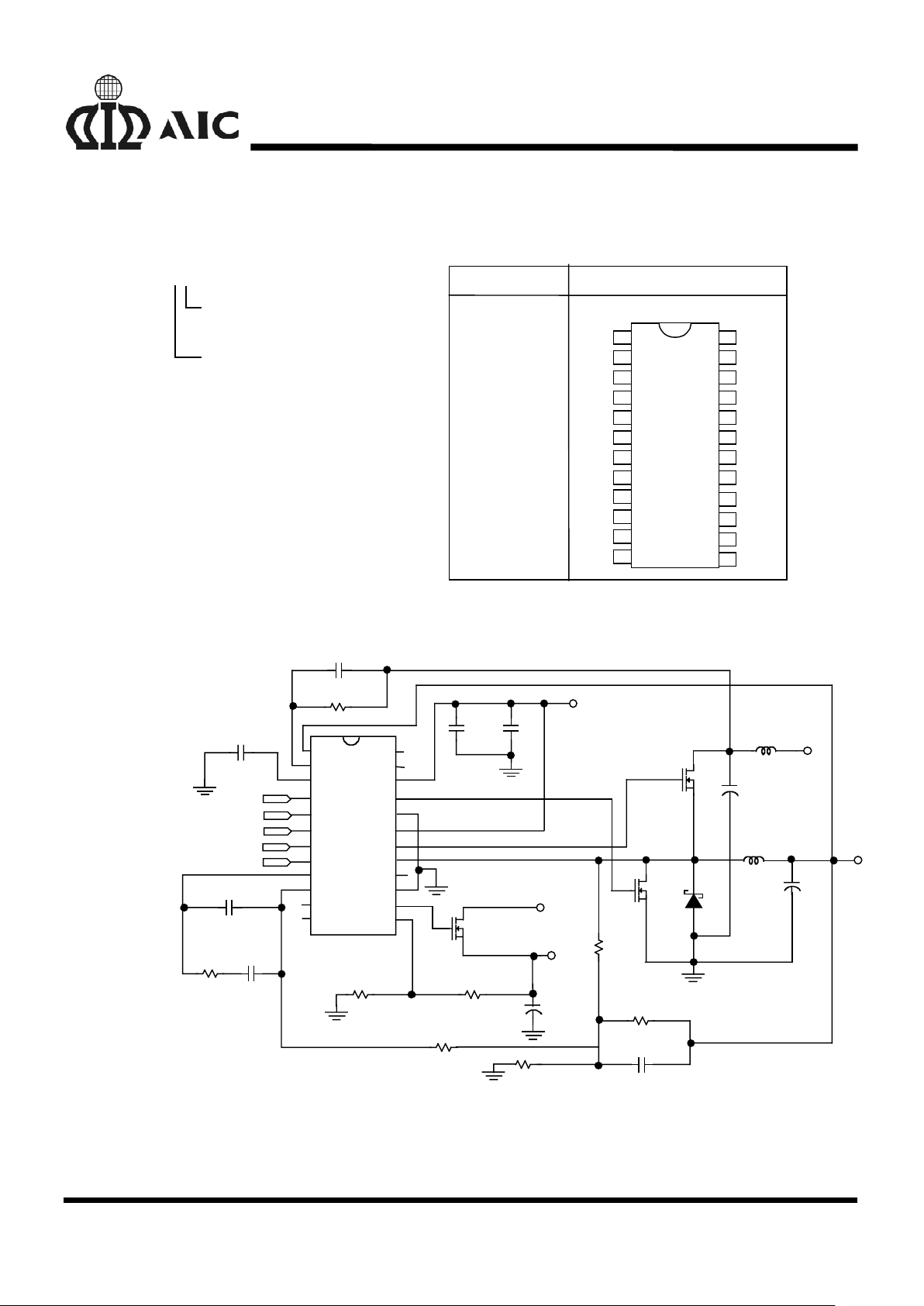
PIN CONFIGURATION
ORDER NUMBER
AIC1567CS
(PLASTIC SO)
TOP VIEW
RT
OVP
VCC
LGATE
PGND
BOOT
UGATE
PHASE
PGOOD
GND
LIDRI
VLFB
24
23
22
21
20
19
18
17
1
2
3
4
5
6
7
8
VSEN
OCSET
SS
VID0
VID1
VID2
VID3
VID4
COMP
FB
CLP
CLN
9
10
11
12
16
15
14
13
TYPICAL APPLICATION CIRCUIT
VSEN RT
OCSET OVP
SS VCC
VID0 LGATE
VID1 PGND
VID2 BOOT
VID3 UGATE
VID4 PHASE
COMP PGOOD
FB GND
CLP LIDRI
CLN VLFB
C2
0.1
µ
F
C1
1
µ
F
C5
1000pF
C7
33pF
C6
1000pF
0.1µF
+
C1
1000
µ
F
5V
137
1%
R3
47K
R5
3.01K
Ω
R6
90.9K
R2
2.2K
C8
R1
237
1%
R7
+
1000µF
x 8
R4
15K
D1
1N5820
M2
NDP603AL
VID0
VID1
VID2
VID3
VID4
V
CORE
V
I/O
3.3V
10A
12V
AIC1567
M3
FD3055
0.1µF
R8
1.2M
C3
1000µF x 3
3µH
L2
M1
RFP45N03L
+
L1
1
µ
H
5V
C4
Pentium
II V
CORE
and V
I/O
DC/DC Converter
AIC1567
3
ABSOLUTE MAXIMUM RATINGS
Supply Voltage, VCC....…..................................……………........................................... 15V
Boot Voltage, V
BOOT
………...................……………...................................................... 15V
Input, Output, or I/O Voltage .....…….........……………......…....... GND - 0.3V to VCC+0.3V
ESD Classification ...........................…………......................……......................... Class 2
Recommended Operating Conditions
Supply Voltage, VCC....…...................…………………..........................…….......... 12V±10%
Ambient Temperature Range ....……………………............................................ 0°C ~ 70°C
Junction Temperature Range ....…………………….......................................... 0°C ~100°C
Thermal Information
Thermal Resistance, θJA (Typical, Note 1)
SOIC Package .....................…….........……………………………….........…. 100°C/W
SOIC Package (with 3 in
2
of Copper) …………………………………......….. 90°C/W
Maximum Junction Temperature (Plastic Package) ….……………….…................... 150°C
Maximum Storage Temperature Range ……………………..……......…......... -65°C~150°C
Maximum Lead Temperature (Soldering 10 sec) …………………………......…......... 300°C
Note 1: symbol
θ
JA
is measured with the component mounted on an evaluation PC board in free air.
TEST CIRCUIT
Refer to TYPICAL APPLICATION CIRCUIT.
ELECTRICAL CHARACTERISTICS (VCC= 12V, Ta=25°
°°
°C, unless otherwise
specified.)
PARAMETER TEST CONDITIONS SYMBOL MIN. TYP. MAX. UNIT
VCC Supply Current
Nominal Supply UGATE Open I
VCC
2mA
Power-On Reset
VCC Threshold V
OCSET
=4.5V 7 8.5 V
Rising V
OCSET
Threshold 1.26 V
Oscillator
Free Running Frequency RT Open 170 200 230 KHz
Total Variation 6KΩ< RT<200KΩ -20 +20 %
Ramp Amplitude RT Open ∆V
OSC
1.5 V
P-P
 Loading...