

AIC AIC1563CS, AIC1563 Datasheet
AIC1563
µ
(%)
(A)
Versatile DC/DC Converter
FEATURES
3V to 30V Input Voltage Operation.
Internal 2A Peak Current Switch.
1.5A Continuous Output Current.
Bootstrapped Driver.
High Side Current Sense Capability.
High Efficiency (up to 90%).
Internal ±2% Reference.
Low Quiescent Current at 1.6mA.
Frequency Operation from 100Hz to 100KHz.
APPLICATIONS
Constant Current Source for Battery Chargers.
Saver for Cellular phones.
Step-Down DC-DC Converter Module.
DESCRIPTION
The AIC1563 is a monolithic control circuit
containing the primary functions required for DC
to DC converters and highside-sensed constant
current source. The device consists of an inter-
nal temperature compensated reference, com-
parator, controlled duty cycle oscillator with an
active current sense circuit, bootstrapped driver,
and high current output switch. This device is
specifically designed to construct a constant
current source for battery chargers with a mini-
mum number of external components. Boot-
strapped driver can drive the NPN output switch
to saturation for higher efficiency and less heat
dissipation. The AIC1563 can deliver 1.5A con-
tinuous current without requiring a heat sink.
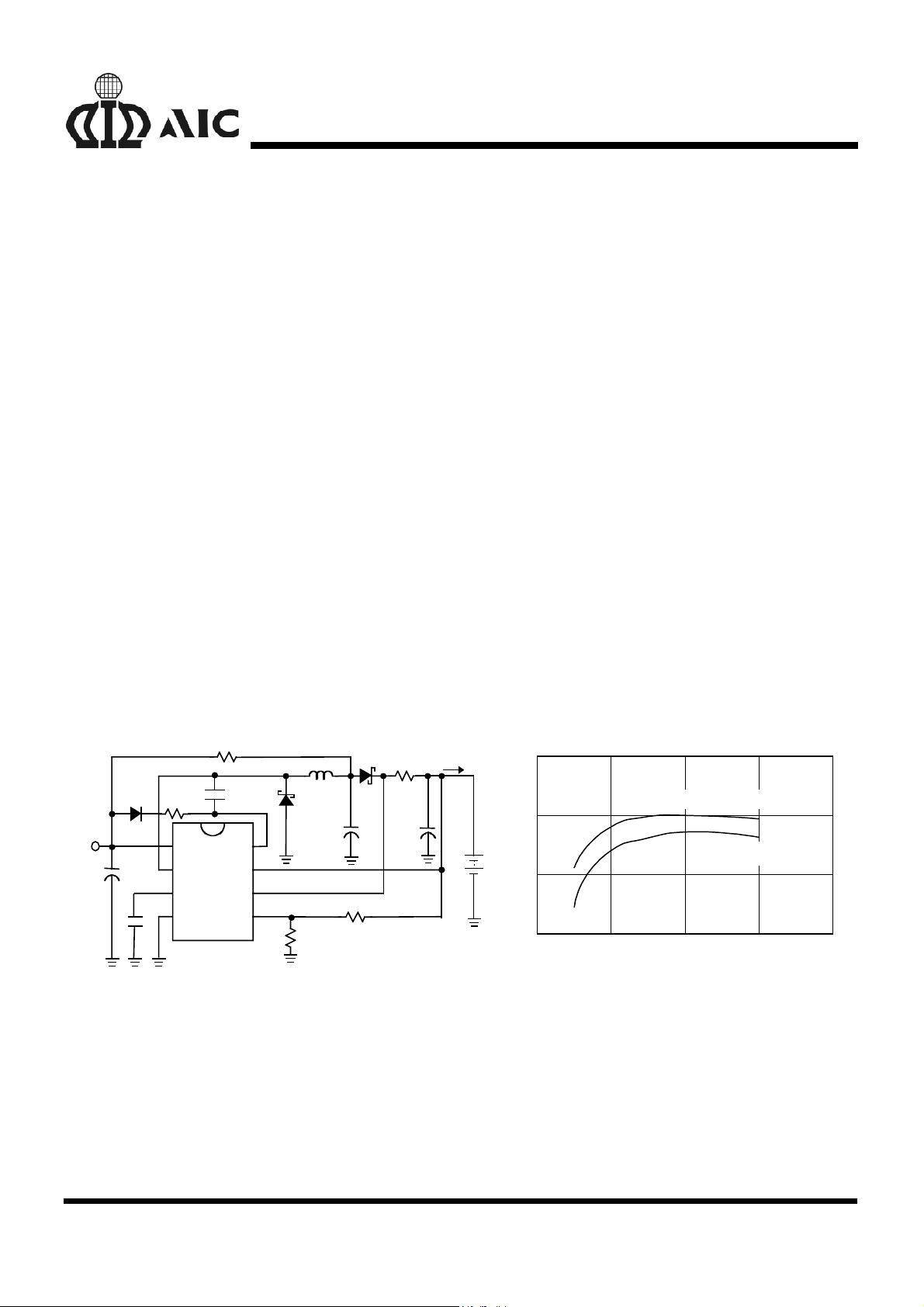
TYPICAL APPLICATION CIRCUIT
R1
1K
BOOST
AIC1563
3C
1µF
IS
VCC
FB
R2
D2
120
1N1418
V
IN
+
220µF
C1
470pF
CT
DC
DE
CF
GND
220
D1
1N5821
RA
5.6K
L
220µF
D3
1N5819
H
+
C
O
RB
33K
*IO=300mV/R S
*RS
10µF
100
I
O
VIN=16V, VO=12V
+
C5
90
VIN=16V, VO=8V
80
70
0 0.5 1 1.5 2
Io
Efficiency vs Output Current
Analog Integrations Corporation 4F, 9, Industry E. 9th Rd, Science Based Industrial Park, Hsinchu Taiwan, ROC www.analog.com.tw
DS-1563-01 Jan 30, 01 TEL: 886-3-5772500 FAX: 886-3-5772510
1
AIC1563
A
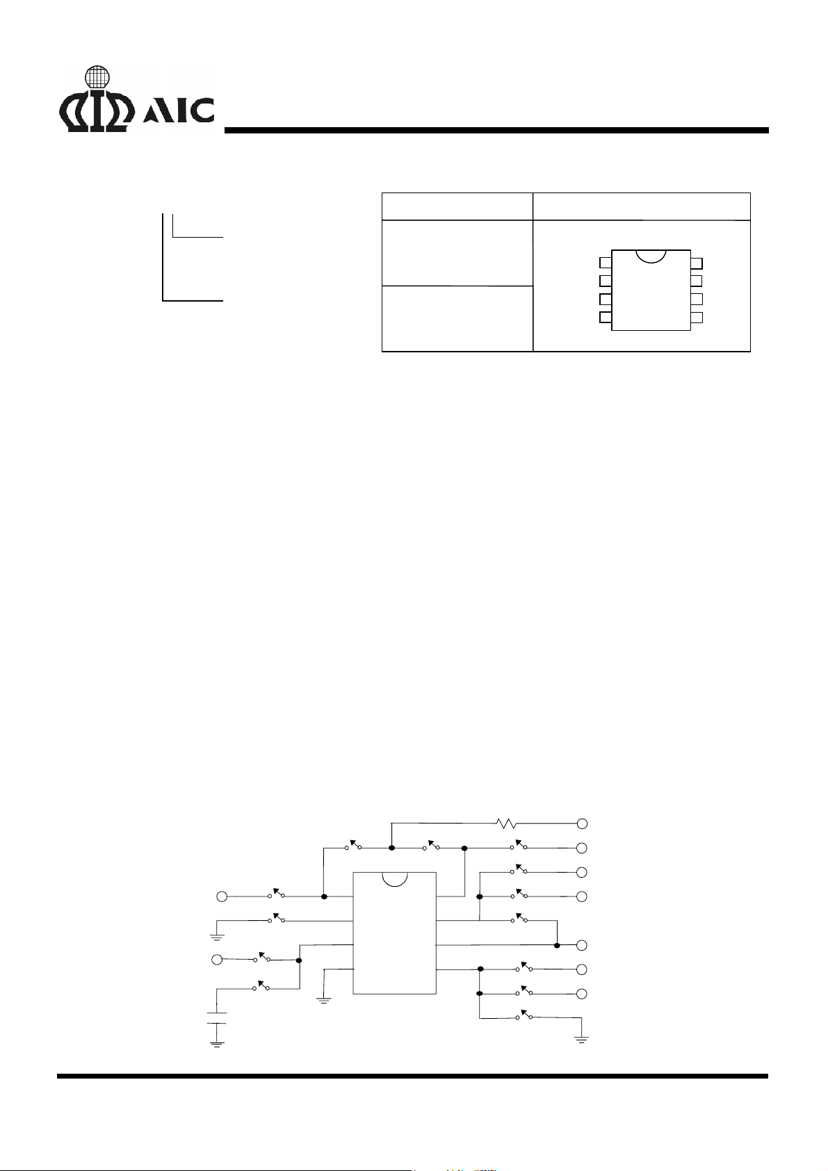
ORDERING INFORMATION
AIC1563 XX
ORDER NUMBER
AIC1563
PIN CONFIGURATION
PACKAGE TYPE
N: PLASTIC DIP
S: SMALL OUTLINE
TEMPERATURE
C: 0°C~+70°C
ABSOLUTE MAXIMUM RATINGS
AIC1563CN
(PLASTIC DIP)
IC1563CS
(PLASTIC SO)
TOP VIEW
DC
DE
CF
GND
Supply Voltage ..............................................................……………............................. 30V
Comparator Input Voltage Range ............................................………….......... -0.3V~30V
Switch Collector Voltage ....................................................……………......................... 30V
Switch Emitter Voltage ......................................................……………......................... 30V
Switch Collector to Emitter Voltage ..................................…………............................. 30V
Driver Collector Voltage ....................................................…………….......................... 30V
Switch Current ................................................………………......................................... 2A
Power Dissipation and Thermal Characteristics
DIP Package
Ta= 25°C ............................…………................................ 1.0W
Thermal Resistance .............…………......................... 100°C/W
SO Package
Ta= 25°C ......................……………............................... 625mW
Thermal Resistance ...................………...................... 160°C/W
Operating Junction Temperature .....................................................………............. 125°C
Operating Ambient Temperature Range .......................……………......................... 0~70°C
Storage Temperature Range ...................................………….................... - 65°C ~ 150°C
1
2
3
4
8
BOOST
7
IS
6
VCC
5
FB
TEST CIRCUIT
R1
VCC
50mA
Current Source
4.55V
@VCC=5V
4.75V
VCC
1.275V
1.225V
2V/0V
I
DISCHG
1A
Current Source
/ I
CHG
1nF
CT
1K
1
DC
2
DE
3
CF
4
GND
AIC1563
BOOST
IS
VCC
FB
8
7
6
5
2
AIC1563
AIC1563
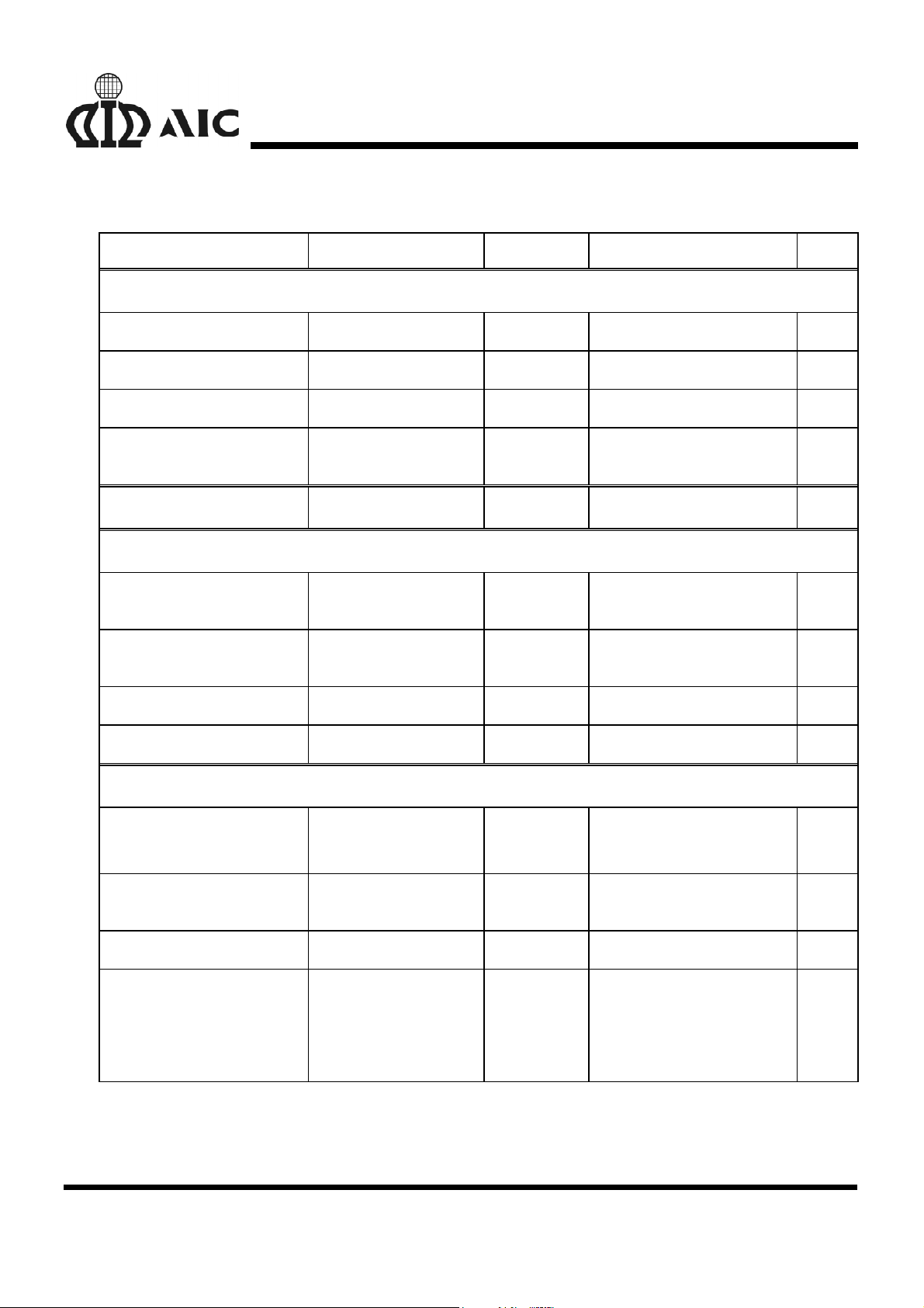
ELECTRICAL CHARACTERISTICS
PARAMETER TEST CONDITIONS SYMBOL MIN. TYP. MAX. UNIT
Oscillator
Charging Current 5.0V≤VCC≤30V I
Discharge Current 5.0V≤VCC≤30V I
Voltage Swing PIN 3 V
Discharge to Charge Current Ratio
Current Limit Sense Voltage I
Output Switch
Saturation Voltage, Emitter
Follower Connection
Saturation Voltage IDC=1.0A; I
VIS =VCC I
CHG=IDISCHG
IDE=1.0A;
V
BOOST
=VDC = VCC
BOOST
=50mA, (Forced β≅20)
(VCC= 5V, Ta=25°°°°C, unless otherwise specified.)
CHG
DISCHG
OSC
DISCHG / ICHG
VCC - V
V
V
CE(SAT)
CE (SAT)
IS
10 25 40 µA
100 150 200 µA
0.6 V
6.0
250 300 350 mV
1.5
0.4
1.8
0.7
V
V
DC Current Gain ISC =1.0A; VCE=5.0V h
Collector Off-State Current VCE=30V I
C(OFF)
Comparactor
Threshold Voltage Ta=25°C
0°C ≤ Ta ≤ 70°C
Threshold Voltage Line
3.0V≤VCC≤30V REG
Regulation
Input Bias Current VIN=0V I
Supply Current VIS =VCC, pin 5>V
FB
5.0V≤ VCC ≤30V
C
=1nF
T
PIN 2=GND
Remaining pins open
FE
35 120
10 nA
V
FB
LINE
IB
I
CC
1.225
1.21
1.25 1.275
1.29
V
V
0.1 0.3 mV/V
0.4 1 µA
1.6 3 mA
3
 Loading...