

AIC AIC1562CS, AIC1562 Datasheet
AIC1562
µ
High-Efficiency, Bootstrapped DC/DC Converter
FEATURES
3V to 20V Input Voltage Operation.
Internal 800mA Switch.
Bootstrapped Driver for N-Channel MOSFET.
High Efficiency (up to 90%).
Fast Transient Response.
Internal ±2% Reference.
Low Quiescent Current at 1.6mA.
Frequency Operation from 200Hz to 200KHz.
APPLICATIONS
CPU Power Supplies for Mother Boards.
DC/DC Converters for CPU VRMs.
Step-Down DC-DC Converter Module.
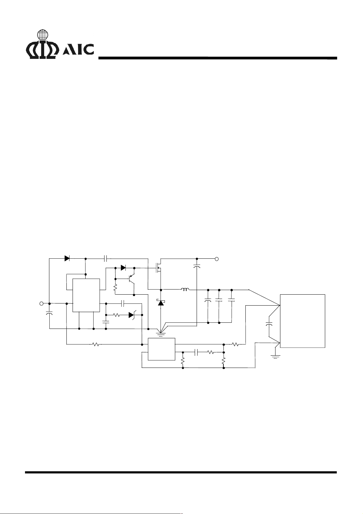
TYPICAL APPLICATION CIRCUIT
C3
1N4148
R2
24K
C2
220pF
D3
R1
1K
0.022µF
C4
Z1
5.1V
Q2
2N2907A
BYV118
VIN
GND
AIC1741
CPU Power Supply for P5 Mother Board
12V
C1
47µF
D2
1N4148
SC
BST
AIC1562
+
VCC
FB
C11, C12: Ceramic Capacitor
L1: Iron Powder Core
V
= (1+R10/1K)x1.235V
OUT
0.1µF
SE
TC
GND
R8
10K
MTD20N03DH
D1
FB
VOUT
DESCRIPTION
The AIC1562 is a high performance monolithic
DC/DC converter drive IC with output-
bootstrapping capability, designed specifically for
driving N-channel MOSFET to achieve maximum
possible power conversion efficiency. The device
consists of an internal temperature compensated
reference, comparator, controlled duty cycle
oscillator, bootstrapped driver and a 800mA output
switch. Working with the AIC1741, a low power
adjustable regulator, the AIC1562 works at 100%
duty cycle under heavy load transient conditions to
minimize transient response time, making it an idea
precision switching power solution to stringent
requirements on computer mother boards.
V
+
F
1000
R8
1K
C10
IN
C11
0.1µF
x2
Q1
L1
7.5µF
R7
470
+
1000µF/6.3Vx2
C8, C9
C5
0.1µF
R9
1K
5V
V
R10
OUT
C12
0.1µF
x2
: 2.5V~3.5V/10A
1000µF/6.3V
x5
C13
MICROPROCESSOR
P5
CPU
+
Analog Integrations Corporation 4F, 9, Industry E. 9th Rd, Science Based Industrial Park, Hsinchu Taiwan, ROC www.analog.com.tw
DS-1562-00 Jan 30, 01 TEL: 886-3-5772500 FAX: 886-3-5772510
1
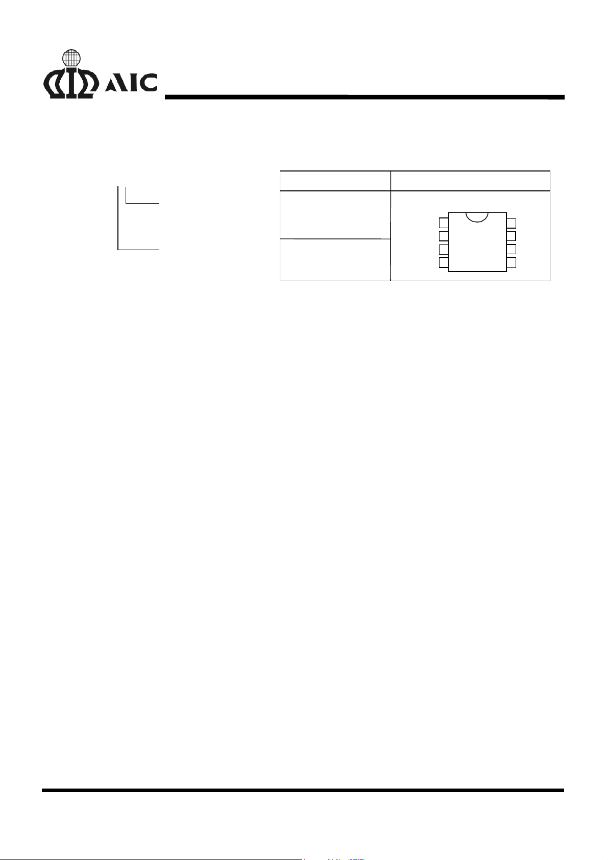
ORDERING INFORMATION
A
AIC1562
IC1562 XX
PACKAGE TYPE
N: PLASTIC DIP
S: SMALL OUTLINE
TEMPERATURE
C: 0°C~+70°C
ORDER NUMBER
AIC1562CN
(PLASTIC DIP)
AIC1562CS
(PLASTIC SO)
PIN CONFIGURATION
TOP VIEW
SC
1
SE
2
3
TC
4
GND
ABSOLUTE MAXIMUM RATINGS
Supply Voltage ...............................................…………………....................................... 20V
Comparator Input Voltage Range .........................…………….............................. -0.3V~20V
Switch Collector Voltage ....................................………………...................................... 20V
Switch Emitter Voltage ......................................…………………................................... 20V
Switch Collector to Emitter Voltage .......................……………..................................... 20V
Driver Collector Voltage .....................................………………..................................... 20V
Switch Current ...............................................................…...………………........…........... 1A
Power Dissipation and Thermal Characteristics
DIP Package
Ta= 25°C ................................…………........................... 1.0W
Thermal Resistance ..........………............................... 100°C/W
SO Package
Ta= 25°C ...........................……………......................... 625mW
Thermal Resistance ...............……….......................... 160°C/W
Operating Junction Temperature .............................…………................................... 125°C
Operating Ambient Temperature Range ...................…………............................ 0°C~70°C
Storage Temperature Range..................…………….................................. - 65°C ~ 150°C
BST
8
7
NC
VCC
6
5
FB
TEST CIRCUIT
2
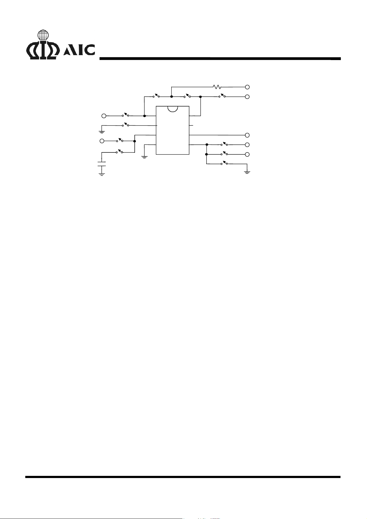
0.8A
Current Source
2V/0V
I
DISCHARG
C
T
AIC1562
R1
1K
1
SC
2
SE
3
TC
4
/ I
CHG
1nF
GND
AIC1562
BST
NC
VCC
FB
8
7
6
5
VCC
40mA
Current Source
VCC
1.275V
1.225V
3
 Loading...