

AIC AIC1523-1CS, AIC1523-1CO, AIC1523-0CS, AIC1523 Datasheet
AIC1523
33µF
5.0V
V
*
0.01µF
+
+
500mA Power Distribution Switch
FEATURES
n
• 120mΩ (5V Input) High-Side MOSFET Switch.
l 500mA Continuous Load Current.
l 80µA Typical On-State Supply Current.
l 1µA Typical Off-State Supply Current.
l Current-Limit / Short Circuit Protection.
l Thermal Limiting Protection under Overcurrent
Condition.
l Output can be Forced Higher than Input (Off-State).
l Active-High or Active-Low Enable.
APPLICATIONS
n
l Power Management.
l PCI Cards With Wake-On- LAN
l Hot Plug-In Power Supplies.
l Power Distribution Switch.
DESCRIPTION
n
The AIC1523 is an integrated high-side power
switches for input power selection applications
that using in portable products or PCI interface
peripheral cards. The high-side switch is a
MOSFET with 120mΩ R
, low voltage drop
DS(ON)
and low power consumption meet power saving
requirements . The switch ON/OFF is controlled
by CTL pin.
Output current is typically limited to 1.0A, well
below the 5A safety requirement, and thermal
shutdown function shuts the switch off to prevent
damage under overcurrent conditions.
Design easily and layout flexibility for getting
stable voltage in power transfer transition for power
selection application. Guaranteed minimum
output rise time limits inrush current during hot
plug-in, minimizing EMI and preventing the voltage
at upstream port from dropping excessively.
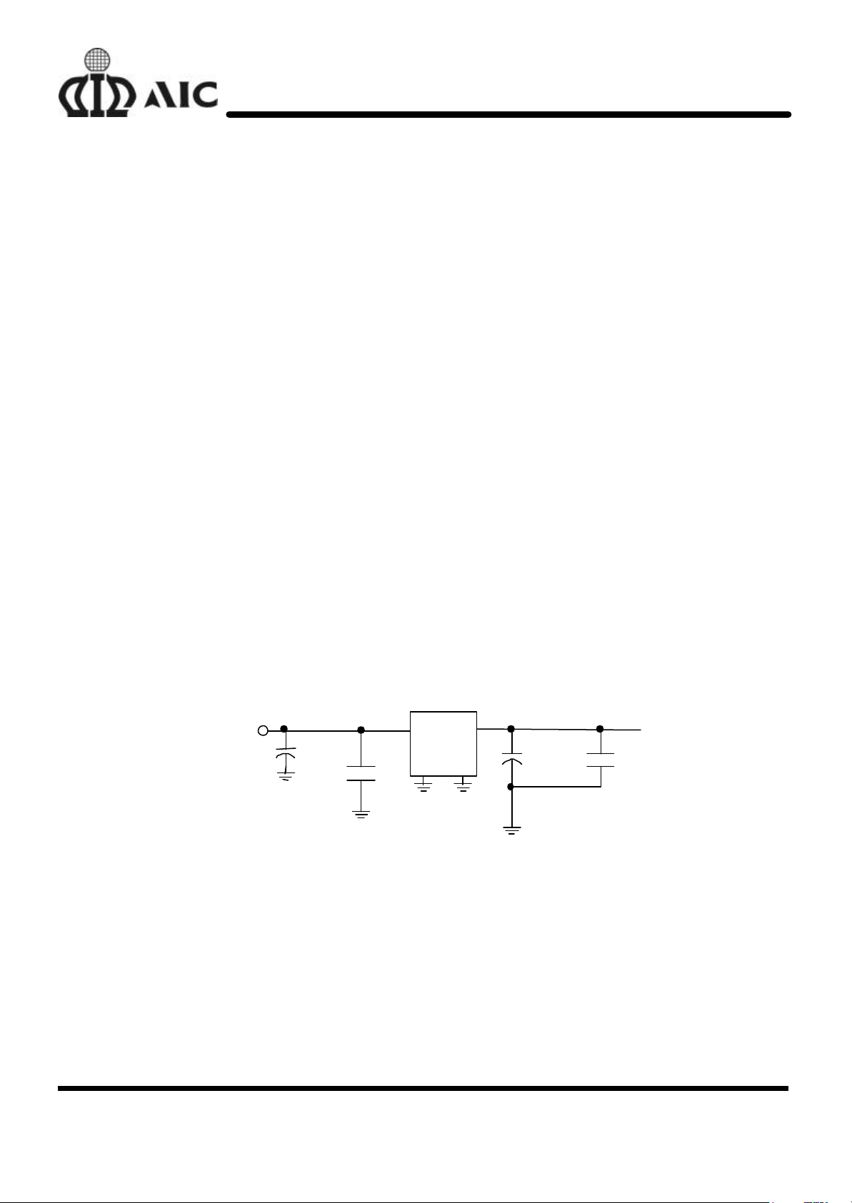
TYPICAL APPLICATION CIRCUIT
n
CC
0.1µF
*33µF, 16V Tantalum, or
100µF, 10V Electrolytic
Bold line indicate high-current traces
High-Side Power Distribution Switch
AIC1523-0
IN
CTL
OUT
GND
33µF
V
OUT
Analog Integrations Corporation 4F, 9, Industry E. 9th Rd, Science Based Industrial Park, Hsinchu Taiwan, ROC
www.analog.com.tw
DS-1523-00 May 30, 01 TEL: 886-3-5772500 FAX: 886-3-5772510 1
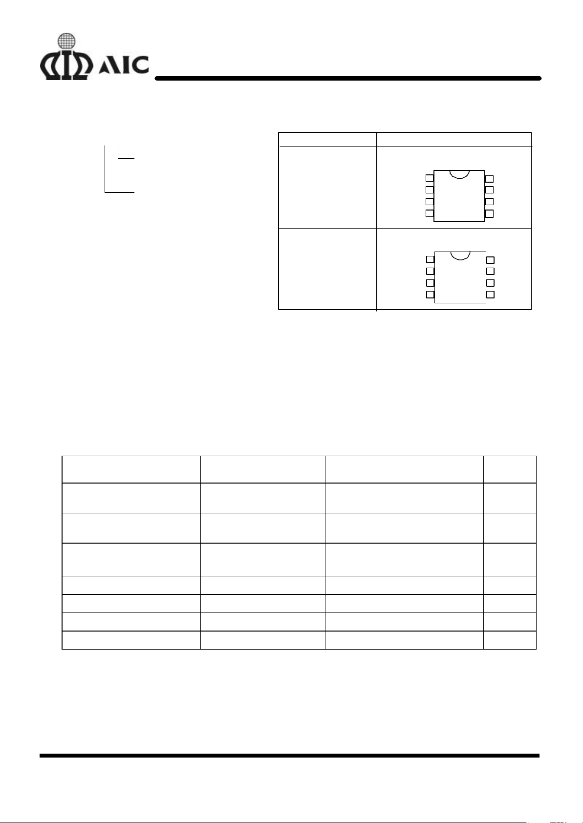
ORDERING INFORMATION
AIC
1523-XCX
OUT
IN
CTL
OUT
CTL
n
AIC1523
ORDER NUMBER PIN CONFIGURATION
PACKAGING TYPE
O: MSOP
S: SO8
CONTROL POLARITY
0: Active Low
1: Active High
AIC1523-0CO
AIC1523-1CO
(MSOP8)
AIC1523-0CS
AIC1523-1CS
(SO8)
FRONT VIEW
FRONT VIEW
ABSOLUTE MAXIMUM RATINGS
n
Supply Voltage (VIN) .......................................................………….......……........... 7.0V
Operating Temperature Range ......………..............…………….…............... -40°C ~ 85°C
Storage Temperature Range ....................................……….................. -65°C ~ 150°C
ELECTRICAL CHARACTERISTICS
n
(VIN= 5V, Ta=25°C, unless otherwise
specified.)
NC
NC
NC 1
IN
NC
1
2
3
4
2
3
4
NC
8
7
NC
6
GND
5
NC
8
7
NC
6
GND
5
PARAMETERS
Supply Current
Control Input Voltage
Control Input Current
Output MOSFET Resistance I
CONDITIONS
Switch Off, OUT=Open
Switch On, OUT=Open
V
=Logic “0”
CTL
V
=Logic “1”
CTL
V
=Logic “0”
CTL
V
=Logic “1”
CTL
= 500mA 120 180 mΩ
OUT
MIN.
2.4
0.01
TYP.
0.75
80
0.01
MAX.
2
100
0.8
1
1
UNIT
µA
V
µA
Output Turn-On Rise Delay RL = 10Ω 30 µS
Output Turn-On Rise Time RL = 10Ω 500 µS
Output Turn-Off Delay RL = 10Ω 0.2 10 µS
2
AIC1523
GATE
RS
2.0 2.5 3.0 3.5 4.0 4.5 5.0 5.5 6.0 6.5 7.0 7.5 50 55
60 65
70 75 80 85 90
Supply Voltage (V)
-
40
-20020406080100
ELECTRICAL CHARACTERISTICS
n
PARAMETERS
Output Turn-Off Fall Time RL = 10Ω 0.2 10 µS
Output Leakage Current 2 µA
Current Limit Threshold Vin = 5.0V 0.6 1.0 1.25 A
Current Limit Threshold Vin = 2.4V 0.6 A
Thermal Limit 110 °C
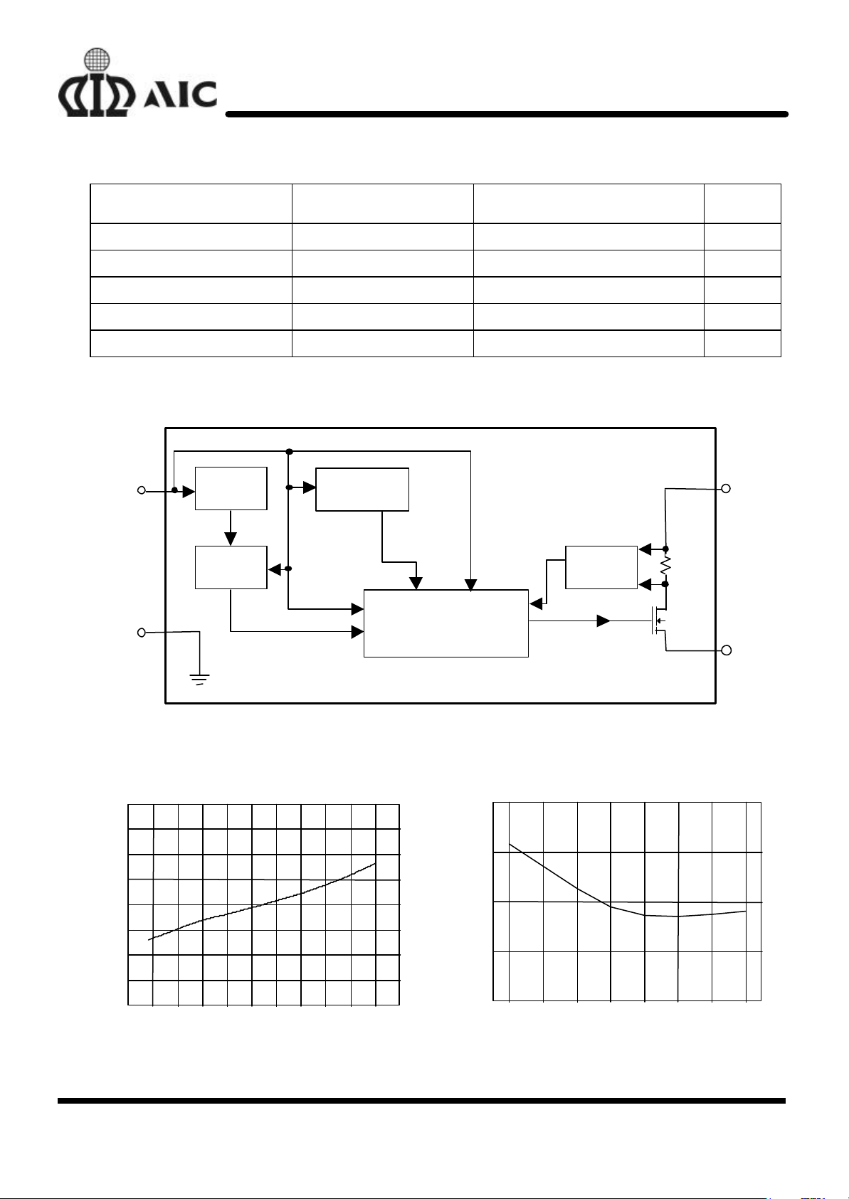
BLOCK DIAGRAM
n
CTL
OSC.
Charge
Pump
CONDITIONS
Thermal
Protection
(Continued)
MIN.
TYP.
Current
Limit
MAX.
UNIT
IN
GND
TYPICAL PERFORMANCE CHARACTERISTICS
n
Supply Current (µA)
On-State Supply Current vs. Supply
Gate Control
On-State Supply Current vs. Temperature
Supply Current (µA)
NMOS
OUT
Temperature (°C)
3
 Loading...