

AIC AIC1340-CS Datasheet

AIC1340
High Performance, Tripple-Ouput, Auto-
Tracking Com bo Controller
Analog Integrations Corporation 4F, 9, Industry E. 9th Rd, Science Based Industrial Park, Hsinchu Taiwan, ROC
www.analog.com.tw
DS-1340-00 May 24, 01 TEL: 886-3-5772500 FAX: 886-3-5772510 1
n
FEATURES
l Provide Triple Accurate Regulated Voltages
l Optimized Voltage-Mode PWM Control
l Dual N-Channel MOSFET Synchronous Drivers
l Fast Transient Response
l Adjustable Over Current Protection using R
DS(on)
.
No External Current Sense Resistor Required.
l Programmable Softstart Function
l 200KHz Free-Running Oscillator
l Robust Output s Auto-Tracking Characteristics
l Sink and Source Capabilities with External Circuit
n
APPLICATIONS
l Advanced PC Mboards
l Information PCs
l Servers and Workstations
l Internet Appliances
l PC Add-On Cards
l DDR Termination.
n
GENERAL DESCRIPTION
The AIC1340 combines a synchronous voltage mode
PWM controller with a low dropout linear regulator
and a linear controller as well as the monitoring and
protection functions in this chip. The PWM controller regulates the output voltage with a synchronous
rectified step-down converter. The built-in N-Channel
MOSFET drivers also help to simplify the design of
step-down converter. It is able to power CPUs,
GPUs, memories, and chipset s. The PWM controller features over current protection using R
DS(on)
. It
improves efficiency and saves cost, as there is no
expensive current sense resistor required.
The built-in adjustable linear controller drives an external MOSFET to form a linear regulator that regulates power for system I/O. The built-in adjustable
low dropout linear regulator can supply current up to
500mA for supplying another system I/O. Output
voltage of both linear regulators can also be adjus ted by means of the external resistor divider. Both
linear regulators feature current limit. With higher
load current required from the low dropout linear
regulator, the AIC1341 is recommended.
The Shutdown function is also provided for disable
the combo controller.
AIC1340
2
n
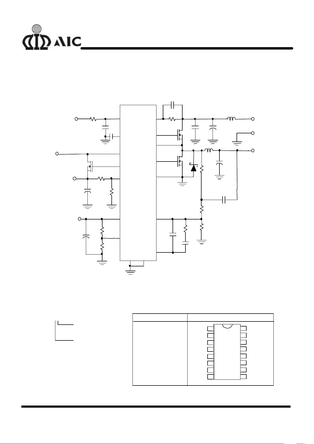
TYPICAL APPLICATION CIRCUIT
+
+
+
UGATE
PHASE
VIN2
LGATE
GATE3
PGND
FB3
VOUT2
FB2
COMP1
SS
GND
+5VIN
VCC
+12VIN
15
OCSET
4
7
11
8
6
2.5V
1.5V
VOUT2
VOUT3
+3.3VIN
12
13
16
1
2
14
14
VOUT1
+
5
GND
FB1
3
SD
10
Typical Triple-Output Application
n
ORDERING INFORMATION
ORDER NUMBER
PIN CONFIGURATION
AIC1340-XX
AIC134 0CS
(SO16)
13425768FB2
UGATE
SD
VCC
PHASE
SS
VIN2
VOUT2
OCSET
LGATE
PGND
FB3
FB1
COMP1
GATE3
GND16141513121
1910
PACKAGING TYPE
S: SMALL OUTLINE
TEMPERATURE RANGE
C: 0°C~+70°C

AIC1340
3
n
ABSOLUTE MAXIMUM RATING
Absolute Maximum Ratings
Supply Voltage (VCC) .....................................................................................................15V
UGATE.........................................................................................GND - 0.3V to VCC + 0.3V
LGATE .........................................................................................GND - 0.3V to VCC + 0.3V
Input Output and I/O Voltage .......................................................................GND - 0.3V to 7V
Operating Conditions
Ambient Temperature Range ...............................................................................0° C to 85°C
Maximum Operating Junction Temperature .................................................................... 100°C
Supply Voltage, VCC ..............................................................................................15V±10%
Thermal Information
Thermal Resistance θJA (°C/W)
SOIC Package..............................................................................................100°C/W
Maximum Junction Temperature (Plastic Package)......................................................... 150°C
Maximum Storage Temperature Range .............................................................-65°C to 150°C
Maximum Lead Temperature (Soldering 10s).................................................................. 300°C
n
TEST CIRCUIT
Refer to APPLICATION CIRCUIT.
 Loading...