

AIC AIC1117A-50CY, AIC1117A-50CT, AIC1117A-50CM, AIC1117A-50CE, AIC1117A-33CY Datasheet
...
1%
1%
AIC1117A
1A Low Dropout Positive Adjustable Regulator
FEATURES
n
l Dropout Voltage 1. 3V at 1A Output Current.
l Fast Transient Response.
l Line Regulation typically at 0.015%.
l Load Regulation typically at 0.1%.
l Internal Thermal and Current Limiting.
l Adjustable Output Voltage or Fixed 2.85V, 3.3V,
5V.
l Standard 3-Pin Power Packages.
APPLICATIONS
n
l Post Regulator for Switching Supply.
l Active SCSI Termination.
l Battery Chargers.
l Constant-Current Regulators.
l Motherboard Clock Supplies.
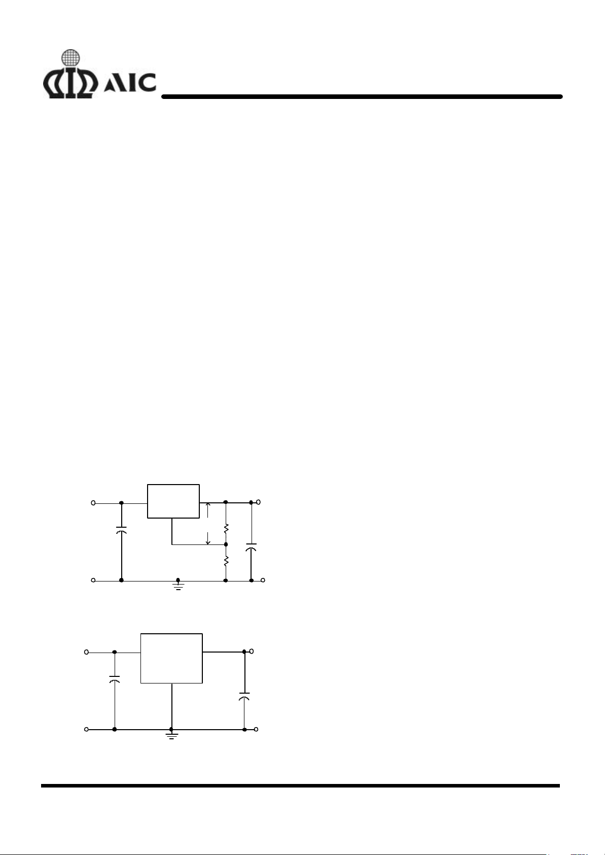
TYPICAL APPLICATION CIRCUIT
n
DESCRIPTION
n
The AIC1117A is a low dropout three terminal
regulator with 1A output current capability. The
output voltage is adjustable with the use of a
resistor divider or fixed 2.85V, 3.3V, 5V . Dropout
is guaranteed at a maximum of 1.5V at
maximum output current. Its low dropout voltage
and fast transient response make it ideal for low
voltage microprocessor applications. Internal
current and thermal limiting provides protection
against any overload condition that would create
excessive junction tem peratures.
V
IN
5V
C1
10µF
AIC1117A
+ V
ADJ
1
Adjustable Voltage Regulator
V
IN
5V
C1
10µF
AIC1117A-33
+
GND
Fixed Voltage Regulator
23
RF2
205
REF
V
V
OUT
3.3V
RF1
Ω
125
+
C2
Ω
10µF
REF=VOUT
V
OUT=VREF
I
=55µA (typ.)
ADJ
(1) C1 needed if device is far away from filter
- V
ADJ
x (1+RF2/RF1)+ I
capacitors.
=1.25V (typ.)
ADJ
x RF2
(2) C2 required for stability.
V
OUT
3.3V
+
C2
10µF
Analog Integrations Corporation 4F, 9, Industry E. 9th Rd, Science Based Industrial Park, Hsinchu Taiwan, ROC www.analog.com.tw
DS-1117A-00 May 21, 01 TEL: 886-3-5772500 FAX: 886-3-5772510 1
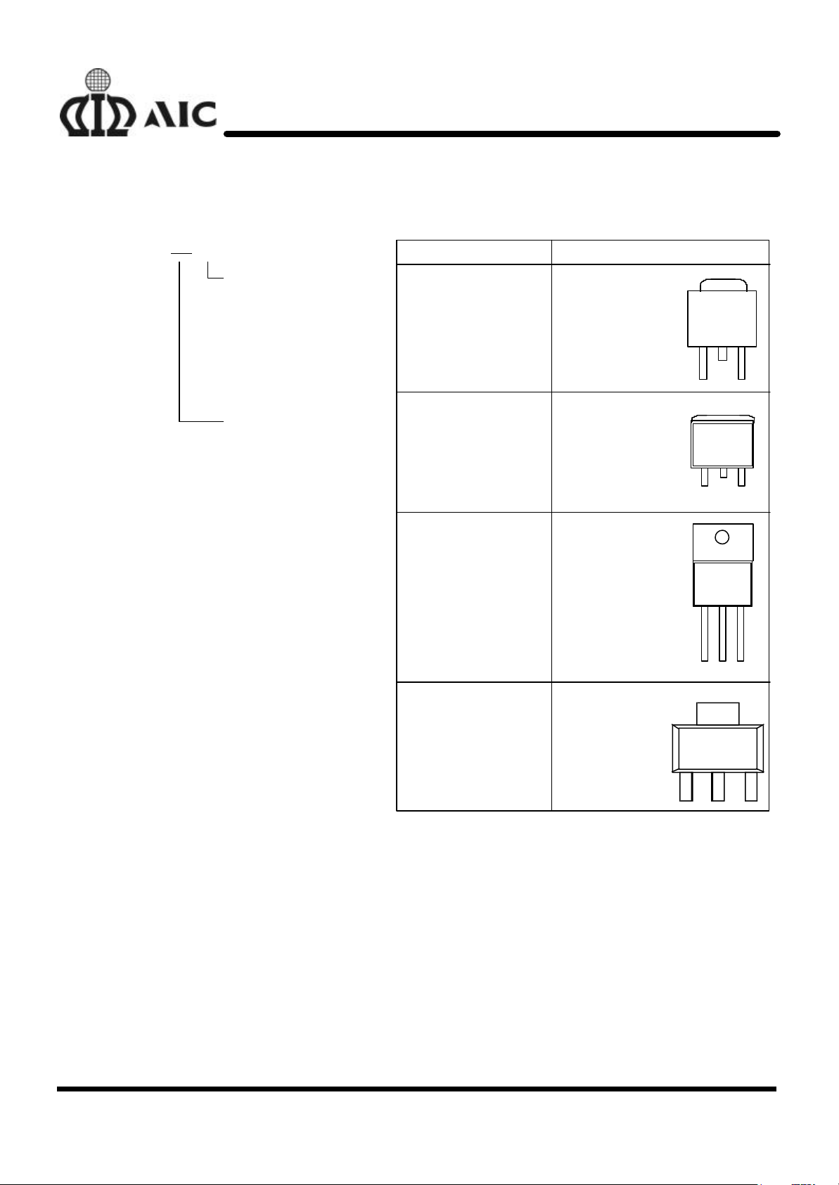
ORDERING INFORMATION
123
231
231
231
n
AIC1117A
AIC1117A-XXCX
PACKAGING TYPE
E: TO-252
M: TO-263
T: TO-220
Y: SOT-223
DEFAULT: ADJ.
28: 2.85V
33: 3.3V
50: 5.0V
ORDER NUMBER
AIC1117ACE
(TO-252)
AIC1117ACM
(TO-263)
AIC1117ACT
(TO-220)
PIN CONFIGURATION
FRONT VIEW
1: ADJ
2: VOUT (TAB)
3: VIN
FRONT VIEW
1: ADJ
2: VOUT (TAB)
3: VIN
FRONT VIEW
1: ADJ
2: VOUT (TAB)
3: VIN
AIC1117ACY
(SOT-223)
FRONT VIEW
1: ADJ
2: VOUT (TAB)
3: VIN
2
ABSOLUTE MAXIMUM RATINS
n
VIN pin to ADJ/GND pin ...........................…….......…….......……………...................... 7V
Operating Junction Temperature Range ..................………...................... 0°C ~ 125°C
Power Dissipation …………………………………………………………….Internally Limited
Thermal Resistance (Junction to Case) TO-220 ………........……...…………... 3°C /W
TO-263 …....……....…………………….3°C /W
SOT-223 …....……..………..………..15°C /W
TO-252 ……………………………..12.5°C /W
Thermal Resistance (Junction to Ambient) TO-220 …....……....………………… 50°C/W
(Assume no ambient airflow, no heatsink) TO-263 ….....…….....………………..60°C/W
SOT-223 ……………………………..155°C/W
TO-252 ……………………………..100°C/W
Storage Temperature Range ...............................…………................. - 65°C ~ 150 °C
AIC1117A
Lead Temperature (Soldering) 10 sec. .....................………............………...….......260°C
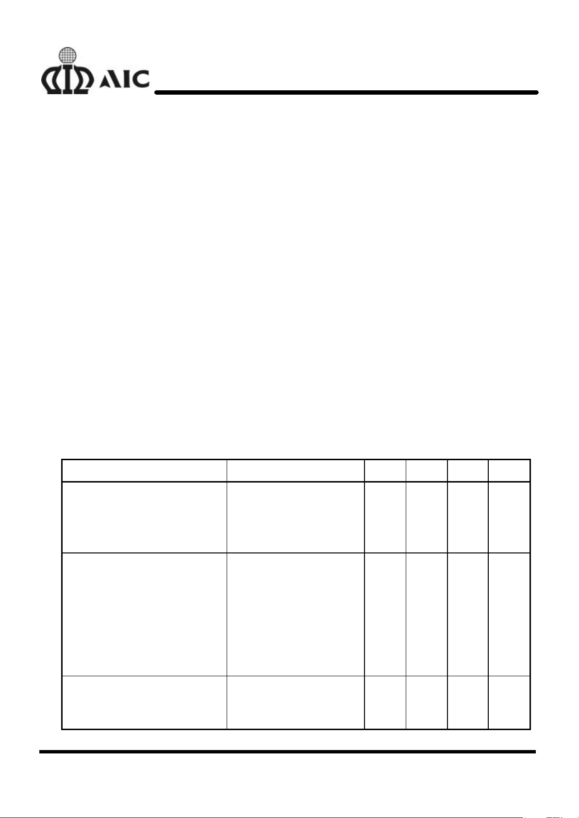
ELECTRICAL CHARACTERISTICS
n
(VIN=5V, TJ=25 °C, IO=10mA, Unless otherwise
specified)
PARAMETER TEST CONDITIONS MIN. TYP. MAX. UNIT
Reference Voltage TJ=25°C
0°C≤TJ≤125°C
2.65V≤VIN≤7V
10mA≤IO≤1A
AIC1117A-28, VIN=5V
AIC1117A-33, VIN=5V
AIC1117A-50, VIN=7V
Output Voltage
AIC1117A
0°C≤TJ≤125°C
1.238
1.225
2.82
3.26
4.95
1.25
1.25
2.85
3.30
5.00
1.262
1.275
V
2.88
3.33
5.05
V
2.65V≤VIN≤7V
10mA≤IO≤1A
2.65≤VIN≤7V
TJ=25°C 0.015 0.2Line Regulation
0°C≤TJ≤125°C 0.035 0.2
0.98V
V
N
1.02V
N
N
%V
OUT
3
 Loading...