

aiAlpha Silicon Schottky Diode Chips Service Manual
Alpha Industries, Inc. [781] 935-5150 • Fax [617] 824-4579 • Email sales@alphaind.com • www.alphaind.com 1
Specifications subject to change without notice. 8/01A
Silicon Schottky Diode Chips
Features
■ For Detector and Mixer Applications
■ Low Capacitance for Usage Beyond 40 GHz
■ ZBD and Low Barrier Designs
■ P-Type and N-Type Junctions
■ Large Bond Pad Chip Design
Description
Alpha’s product line of silicon Schottky diode chips are
intended for use as detector and mixer devices in hybrid
integrated circuits at frequencies from below 100 MHz to
higher than 40 GHz. Alpha’s “Universal Chip” design
features a 4 mil diameter bond pad that is offset from the
semiconductor junction preventing damage to the active
junction as a result of wire bonding.
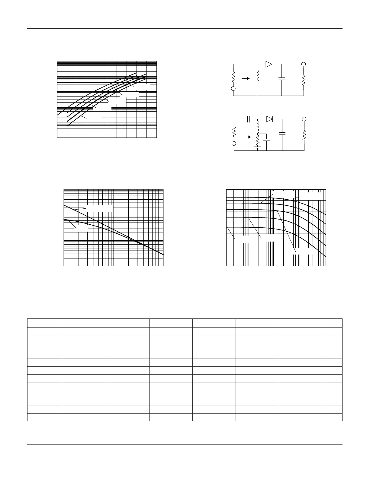
As power-sensing detectors, these Schottky diode chips
all have the same voltage sensitivity so long as the output
video impedance is much higher than the video
resistance of the diode. Figure 1 shows the expected
detected voltage sensitivity as a function of RF source
impedance in an untuned circuit. Note that sensitivity is
substantially increased by transforming the source
impedance from 50 Ω to higher values. Maximum
sensitivity occurs when the source impedance equals the
video resistance.
Electrical Specifications at 25°C
Junction
C
J
1
R
T
2
VF@ 1 mA V
B
3
RV@ Zero Bias
Outline
Part Number Barrier
Type
(pF) (ΩΩ) (mV) (V) (kΩΩ)
Drawing
Max. Max. Min.–Max. Min. Typ.
CDC7630-000 ZBD P 0.25 30 135–240 1 5.5 526-006
CDC7631-000 ZBD P 0.15 80 150–300 2 7.2 526-006
CDB7619-000 Low P 0.10 40 275–375 2 735 526-006
CDB7620-000 Low P 0.15 30 250–350 2 537 526-006
CDF7621-000 Low N 0.10 20 270–350 2 680 526-011
CDF7623-000 Low N 0.30 10 240–300 2 245 526-011
1. CJfor low barrier diodes specified at 0 V. CJfor ZBDs specified at 0.15 V
reverse bias.
2. R
T
is the slope resistance at 10 mA. RSMax. may be calculated from:
R
S
= RT- 2.6 x N.
3. V
B
for low barrier diodes is specified at 10 µA. VBfor ZBDs is specified
at 100 µA.
In a detector circuit operating at zero bias, depending on
the video load impedance, a ZBD device with RVless than
10 kΩ may be more sensitive than a low barrier diode with
RVgreater than 100 kΩ. Applying forward bias reduces
the diode video resistance as shown in Figure 2. Lower
video resistance also increases the video bandwidth but
does not increase voltage sensitivity, as shown in
Figure 3. Biased Schottky diodes have better temperature
stability and also may be used in temperature
compensated detector circuits.
P-type Schottky diodes generate lower 1/F noise and are
preferred for Doppler mixers and biased detector
applications.The bond pad for the P-type Schottky diode
is the cathode. N-type Schottky diodes have lower parasitic
resistance, RS, and will perform with lower conversion loss
in mixer circuits. The bond pad for the N-type Schottky
diode is the anode.
查询CDB7619-000供应商
Silicon Schottky Diode Chips
2 Alpha Industries, Inc. [781] 935-5150 • Fax [617] 824-4579 • Email sales@alphaind.com • www.alphaind.com
Specifications subject to change without notice. 8/01A
SPICE Model Parameters
Parameter CDB7619 CDB7620 CDF7621 CDF7623 CDC7630 CDC7631 Units
IS 3.70E-08 5.40E-08 4.0E-08 1.1E-07 5.0E-06 3.8E-06 A
R
S
9 14 12 6 20 51 Ω
N 1.05 1.12 1.05 1.04 1.05 1.05
TT 1E-11 1E-11 1E-11 1E-11 1E-11 1E-11 S
C
J0
0.08 0.15 0.10 0.22 0.14 0.08 pF
M 0.35 0.35 0.35 0.32 0.40 0.4
E
G
0.69 0.69 0.69 0.69 0.69 0.69 eV
XTI 2.0 2.0 2.0 2.0 2.0 2.0
F
C
0.5 0.5 0.5 0.5 0.5 0.5
B
V
2.0 4.0 3.0 2.0 2.0 2.0 V
I
BV
1.00E-05 1.00E-05 1.0E-05 1.0E-05 1.0E-04 1.0E-04 A
V
J
0.495 0.495 0.495 0.495 0.340 0.340 V
0.1
1
10
100
1000
10000
-40 -30 -20 -10 0 10
Input Power (dBm)
Detected Voltage (mV)
25 Ω
50 Ω
100 Ω
200 Ω
500 Ω
Typical Performance Data
100
1000
10000
100000
1 10 100
Forward Bias (µA)
Video Resistance (Ω)
ZBD
Low Barrier
RF SOURCE
IMPEDANCE
DETECTOR
VOLTAGE
VIDEO LOAD
IMPEDANCE
RFC
P
Input
Zero Biased Detector
RF SOURCE
IMPEDANCE
DETECTOR
VOLTAGE
VIDEO LOAD
IMPEDANCE
RFC
P
Input
Biased Detector
0.001
0.01
0.1
1
10
100
1000
10000
0.001 0.01 0.1 1 10
Forward Current (mA)
Detected Voltage (mV)
-30 dBm
-20 dBm
-10dBm
0 dBm
+10 dBm
Figure 1. Detected Voltage vs. Input
Power and RF Source Impedance
Figure 3. Detected Voltage vs. Forward CurrentFigure 2. Video Resistance vs. Forward Bias Current
 Loading...