

Page 1
Agilent AN 372-1
Power Supply Testing
Application Note
An electronic load offers a broad range of
operating modes, providing versatile loading
configurations needed for characterizing and
verifying DC power supply design specifications.
Page 2

2
As regulated-power supply technology evolves,
testing methods for design verification and product
function require more sophisticated electronic equipment. The different power supply architectures
and output combinations also dictate the need for
versatile test instruments that can accommodate a
broad range of specifications. As a result, one testing requirement that has been growing in importance is the method of loading the power supply
under test. The need for a higher degree of load
control due to test sophistication, such as the need
for computer programmability, has increased the
demand for electronic load instruments. The following examination of the most common power supply
architectures or topologies clearly illustrates the
growing need for higher performance and versatility
in electronic loads and power supply test equipment.
An Overview of Power Supply Topologies
Of all the possible power supply topologies, linear
and switching regulation techniques are the most
common design implementations. Linear power
supplies are typically used in R&D environments
and in production test systems because they provide high performance, low PARD (ripple and noise),
excellent line and load regulation, and superior
transient recovery time specifications. However,
they are relatively inefficient when compared to
switching power supplies, and tend to be large
and heavy due to the heat sinks required to continuously dissipate power from the series transistors
and due to the magnetics used in this design. Typically, linear power supplies provide a most effective solution in lower power applications, and are
often used as subassemblies in various products.
Switching power supplies address the disadvantages of linear power supplies (namely the low efficiency and relatively large size and weight), and
are therefore a more effective and less costly solution for high power applications. The relative disadvantages occur in three areas when compared to
linear power supplies: slower transient recovery
time, higher PARD, and lower reliability. Switching
power supplies are used in a wide variety of industries and environments, and are commonly found
as subassemblies in products such as computers,
computer peripherals, and copiers. Recent power
supply designs combine the best features of switching and linear topologies. Below, Table 1 compares
the typical specifications for linear and switching
topologies.
Introduction
Table 1
Regulation Load Line Transient
Technique Regulation Regulation Response PARD Efficiency
Switching 0.05 – 0.5% 0.05 – 0.5% 1 – 20 ms 5 – 20 mVrms 65 – 85%
20 – 150 mVp-p
Linear 0.005 – 0.1% 0.005 – 0.1% 20 – 200 µs 0.25 – 5 mVrms 30 – 50%
(Series Pass) 1.0 – 15 mVp-p
Page 3

3
Power supplies are used in a wide variety of products and test systems. As a result, the tests performed to determine operating specifications can
differ from manufacturer to manufacturer, or from
end user to end user. For instance, the tests performed in an R&D environment are primarily for
power supply design verification. These tests
require high performance test equipment and a
high degree of manual control for bench use. In
contrast, power supply testing in production environments primarily focus on overall function based
on the specifications determined during the products design phase. Automation is often essential
due to large volume testing, which requires high
test throughput and test repeatability. Power supply test instruments must then be computer programmable. For both test environments, measurement synchronization is necessary to perform some
tests properly and to obtain valid data. In addition,
considerations such as test set reliability, protection of the power supply under test, rack space,
and total cost of ownership may be of equal importance to the power supply test set designer. Proper
selection of testing instrumentation will provide
the best combination of measurement sophistication and test set complexity.
Power Supply Testing Instrumentation
The power supply testing methods and configurations discussed in this application note are certainly not the only means of obtaining the desired
measurements. However, certain instruments are
essential to all tests, regardless of the implementation. Some commercially available turnkey power
supply test systems incorporate custom board level
instrumentation and hand wiring. However, power
supply test systems based on standard products
afford greater benefits. These systems are more
reliable and provide repeatable, high performance
measurements because of their low noise environment. A system which utilizes standard instrumentation is modular, allows configuration flexibility
based on performance needs, and is easier to
upgrade. In addition, the service, replacement, or
calibration of separate instruments in the system
can be performed with minimal system down-time.
The tests covered in the following section are configured with standard instrumentation: electronic
loads, digital oscilloscopes, digital multimeters,
true rms voltmeters, wattmeters, and AC power
sources.
Electronic loads can facilitate power supply testing
in several ways. They are typically programmable,
although most require external DAC programmers.
This capability enables finer control over loading
values during testing, and can provide the test set
operator with valuable status information. These
loads are often designed with FETs, which provide
increased reliability over less sophisticated solutions consisting of relays and resistors. Also, these
products offer a selection of operating modes:
constant current (CC), constant voltage (CV), and
constant resistance (CR). The more sophisticated
electronic loads provide all three modes in one
product for optimum testing flexibility. They provide a versatile solution for testing both DC voltage
and current sources. A final advantage is provided
by loads with readback over the bus. This can eliminate the need for digital multimeters for voltage
and current measurements in some tests. As mentioned, there are varying degrees of electronic load
sophistication. The Agilent Electronic Load family
provides all of the most sophisticated features and
high level performance in one box.
Several other instruments are required for power
supply testing. The performance criteria (accuracy,
resolution, stability, bandwidth, etc.) vary for each
test. In general, the measurement capability of the
instruments should ensure an error no greater than
10% of the measured specification. Table 2 on the
next page provides a guideline for instrument performance levels for each test discussed in this
application note.
An Overview of Power Supply Testing Needs
Page 4
4
Load Transient Recovery Time
A constant voltage DC power supply is designed
with a feedback loop which continuously acts to
maintain the output voltage at a steady-state level.
The feedback loop has a finite bandwidth, which
limits the ability of the power supply to respond
to a change in the load current. If the time delay
between the power supply feedback loop input and
output approaches a critical value at its unity gain
crossover, the power supply will become unstable
and oscillate. Typically, this time delay is measured
as an angular difference and is expressed as a degree
of phase shift. The critical value is 180 degrees of
phase shift between the loop input and output.
Power Supply Tests
Table 2
Load Transient Current Limit Efficiency and
Recovery Time Load Effect Characterization PARD Power Factor Start-Up
Electronic Load t
rise
≤15 µs 1% programming 1% programming 1% programming 1% programming 1% programming
accuracy accuracy accuracy accuracy accuracy
Trigger output to CC or CR mode CR or CC mode CC or CR mode CC or CV mode CR mode
the oscilloscope Low PARD
Digital t
sample
≤100 ns N/A N/A t
sample
≤25 ns N/A t
sample
≤1 µs
Oscilloscope DC to 20 MHz Record length 1 K
minimum bandwidth samples minimum
Record length
≥2 K samples
100 µ/Div (linears)
1 mV/Div (switchers)
Digital N/A 51/2 Digits 51/2 Digits N/A N/A N/A
Multimeter ±0.005% accuracy ±0.005% accuracy
Wattmeter N/A N/A N/A N/A 1% accuracy with N/A
crest factors to
10:1 in current
waveforms
Regulated >1% regulation >1% regulation N/A >1% regulation >1% regulation >1% regulation
AC Source Adjustable peak Adjustable peak Adjustable peak Adjustable peak Adjustable peak
and frequency and frequency and frequency and frequency and frequency
Power factor Phase control
measurement
capability
RF rms N/A N/A N/A 100 µV Full scale N/A N/A
Voltmeter DC to 20 MHz
minimum bandwidth
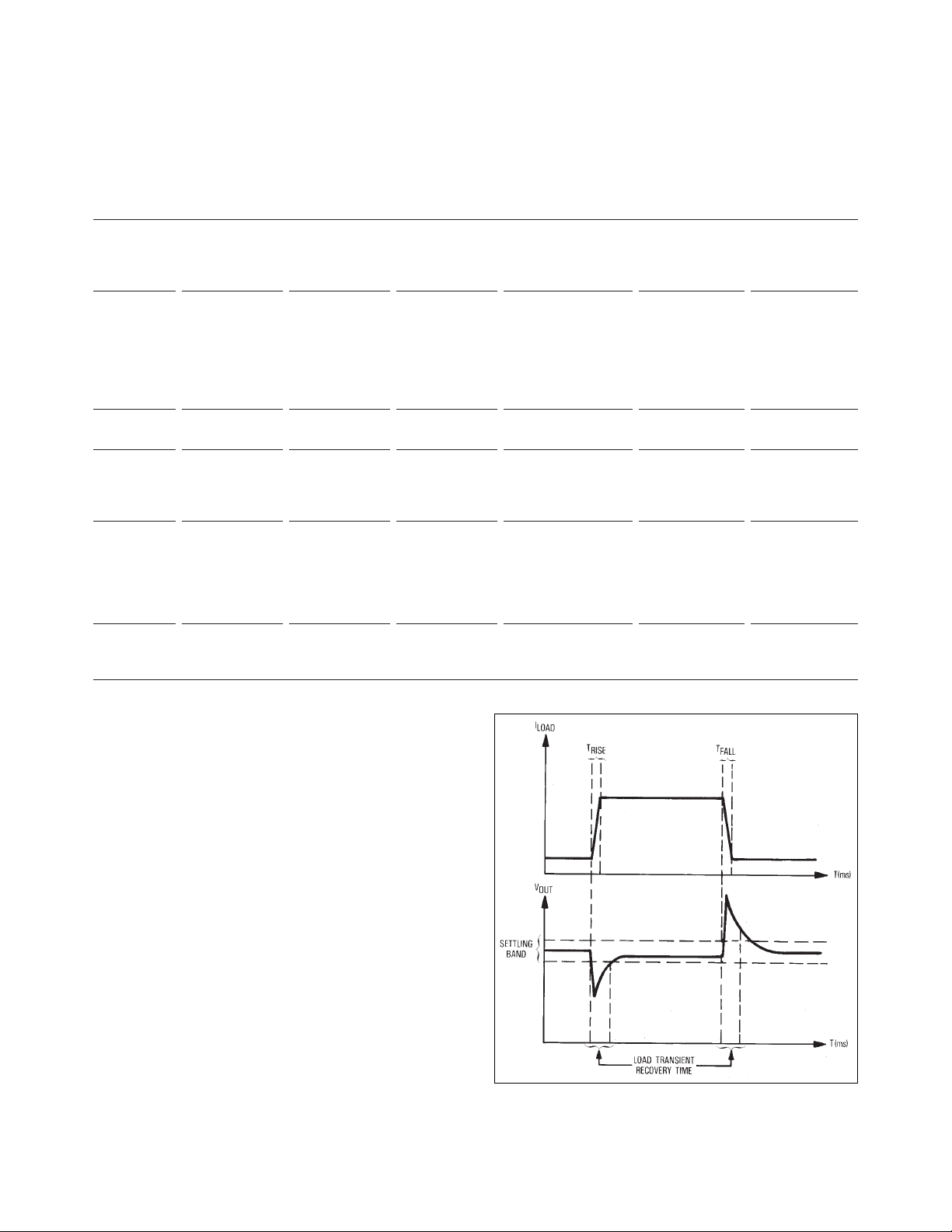
Figure 1. Load Transient Recovery Time
Load transient recovery time measurements require an electronic
load with a risetime and falltime at least five times faster than the
power supply under test.
Page 5
5
For a step change in load current, a marginally
stable CV power supply will have a ringing voltage
output. This defeats the purpose of the power supply’s regulation circuitry and can be damaging
to voltage-sensitive loads. An example of a voltagesensitive load is the logic circuitry in a computer.
In this case, a computer manufacturer that purchases power supplies from an external source may
consider verifying the load transient recovery specification of the power supply subassembly. This
test can also reveal critical manufacturing flaws
that can cause instability, such as a defective output filter capacitor or loose capacitor connections.
Test Overview/Procedures
CV Load Transient Recovery Time is a dynamic
measurement of the time required for the output
voltage of a CV power supply to settle within a
predefined settling band following a load current
induced transient (see Figure 1). The response is
typically measured in microseconds or milliseconds,
and varies in value depending on the topology of
the power supply under test. The electronic load
used in this test should have a risetime at least
five times faster than the power supply under test,
and should be able to operate in CC mode (or CR
mode) up to the maximum current rating of the
power supply. Measuring the load transient recovery time requires the load to have the capability
to pulse between two different values in CC or CR
mode. For continuous load transient testing, the
repetition rate of the pulses should be slow enough
so that the power supply feedback loop can recover
and stabilize after each applied transient.
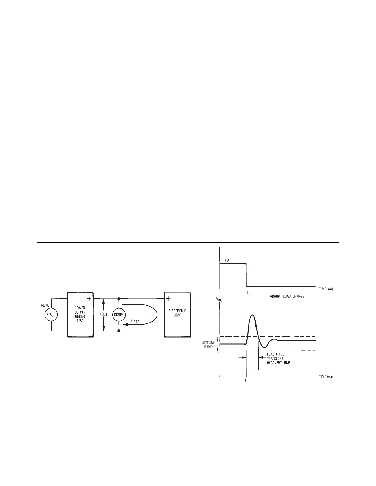
Figure 2 shows a typical test system for making load
transient recovery time measurements. Measurement of V
out
of the power supply can be made with
a digitizing oscilloscope as the load input pulses
are applied. Synchronization of the measurement
is crucial in obtaining proper measurements. Therefore, a common trigger should start the electronic
load and oscilloscope measurements.
Figure 2. Load Transient Recovery Test Configuration and V
OUT
Measurement Results for a CV Power Supply
Page 6

6
Load Effect (Load Regulation)
Load Effect or Load Regulation is a static performance measurement which defines the ability of a
power supply under test to remain within specified
output limits for a predetermined load change (see
Figure 3). In a CV power supply, the influenced
quantity of interest is the steady-state output current. In a CC power supply, the influenced quantity
is the steady-state output voltage. For single output
CV power supplies, voltage load effect is given for a
load current change equal to the current rating of
the supply. A typical specification would be stated
in millivolts, or as a % of the rated output voltage.
For multiple output CV power supplies, cross
load effect is determined. This is an extension of
the load effect test for a single output power supply, and determines the ability of all outputs of a
CV power supply to remain within their specified
voltage rating for a load current change on one
output. Conversely, the ability of one output to
withstand the effects of changes on all other outputs can be specified.
Test Overview/ Procedures
For a CV power supply, measurement of the output
voltage and input voltage should be made after the
load is varied from the minimum to the full current
rating of the power supply under test (Figure 4).
Measurement of the AC input voltage is necessary
to ensure that the output voltage change is a result
of only the load change, and not from a change in
the AC input. To decrease the test time when test
throughput is a concern, a regulated AC source
providing a predetermined AC input level and frequency can be utilized. This will eliminate the need
for the AC input voltage measurement.
The output voltage should be allowed the specified
settling time before measurements are taken. An
electronic load selected for this test must be capable of operating in CC or CR mode, and must have
input ratings (voltage, current, and power) sufficient to accommodate the maximum ratings of the
power supply under test.
Figure 3. Load Effect
For a load current change equal to the full current rating of a CV
power supply, the resulting change in V
OUT
should not exceed the
predetermined load effect band. Typical specifications for load
effect range from 0.005 to 0.5% of the maximum output voltage.
Figure 4. Load Effect Testing Configuration
A regulated AC source is used in this load effect testing configuration to maintain the AC input at a predetermined
value. This will ensure that the test results reflect changes in V
OUT
only with respect to load current changes.
Page 7
7
Current Limit Characterization
Current limit measurements demonstrate the degree
to which a constant voltage power supply limits its
maximum output current to a preset value. This
preset value can be fixed or variable throughout a
specified range. There are basically three types of
current limiting design implementations:
1. Conventional current limiting power supplies
2. CV/CC mode power supplies
3. Foldback current limiting power supplies
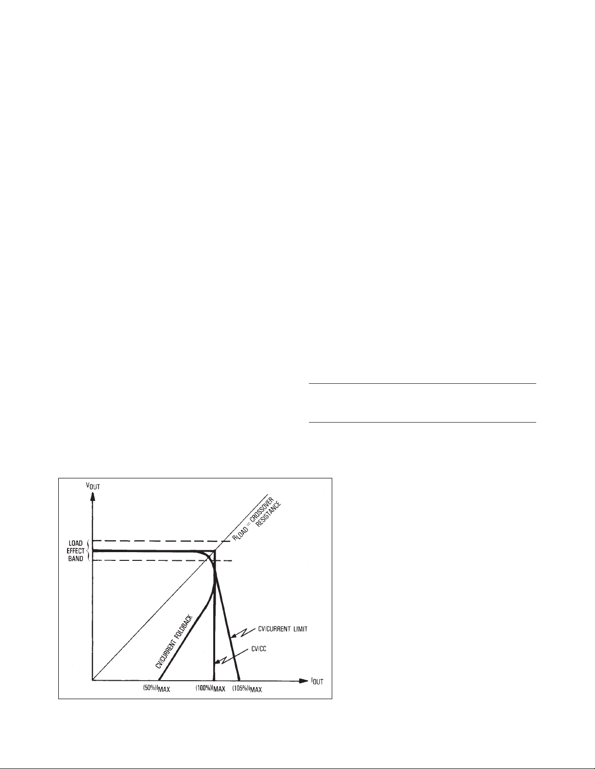
Conventional current limiting power supplies
and CV/CC mode power supplies are very similar
in function. These implementations generally vary
only in the degree of regulation in the constant
current operating region (see Figure 5) and in the
ability of the user to adjust the CC operating point
(CV/CC power supplies). A rounded crossover knee
and sloping current limit characteristic denotes
less precise current regulation. In comparison, a
sharp knee and vertical current limit characteristic
denote a higher degree of current regulation. The
foldback current limiting power supply employs a
technique that enables both the output voltage and
current to decrease simultaneously for load resistances below the crossover value. The purpose of
current limiting is to provide protection for the
power supply and the device being powered (assuming the current limit value is below the maximum
current rating of the device).
Test Overview/ Procedures
A measurement of the output voltage and current
of the power supply under test is required while
decrementing the electronic load resistance (or
current in CC mode) by steps from an initial value
that produces the power supply’s full rated voltage
output (see Figure 6). The voltage will remain constant until the compliance current (output current
of the power supply) increases to the preset current
limit value. The crossover region or current limit
has been reached when the rated output voltage of
the power supply changes by a degree greater than
the load regulation specification. At the current
limit knee, the compliance current and output voltage behavior is determined by the type of current
limiting circuit implemented in the power supply
design (see Table 3).
Table 3. Typical Test Results of Standard Current
Limiting Implementations
I Compliance (or I
out
)
Current Limiting Method at Minimum Load Resistance
CV/CC Remain constant (CC mode)
Conventional Current Limiting Typically ≤(105%) I
max
Current Foldback Typically foldback is ≤(50%) I
max
Figure 5. Typical Operating Characteristics of Three Types of Current
Limiting Power Supplies
Page 8

8
PARD (Periodic and Random Deviation)
PARD (formerly known as ripple and noise) is the
periodic and random deviation of the DC output
voltage from its average value, over a specified
bandwidth, and with all other parameters constant. It is representative of all undesirable AC and
noise components that remain in the DC output
voltage after the regulation and filtering circuitry
(see Figure 7).
PARD is measured in rms or peak-to-peak values,
and is typically specified over a bandwidth range
of 20 Hz to 20 MHz. Any deviation below 20 Hz is
included in a specification called output drift. In
some applications, a low output ripple specification is critical. An example would be where the
power supply is providing power to a high gain
amplifier with inadequate ripple rejection for the
application. In this case, a portion of the power
supply PARD would be amplified along with the
desired signal. It is extremely important that the
PARD value be specified as a peak-to-peak value
as well as an rms value in this application. The
peak-to-peak value would provide information on
high magnitude, short duration noise spikes while
the rms value would be beneficial for determination of the expected signal-to-noise ratio.
Figure 6. Test Configuration and Results for Current Limit Characterization
Figure 7. PARD Consists of Undesirable Signals Superimposed on the DC Output of
a Power Supply
Page 9

9
Test Overview/Procedures
To make PARD measurements, the electronic load
used should operate in CR mode for constant voltage and constant current power supplies. The load
should also have lower PARD than the power supply being tested. This is especially important when
measuring the PARD of linear power supplies, since
they typically have excellent PARD specifications.
A regulated AC source should be applied to the
input of the power supply under test. PARD measurements are made at the lowest and highest specified values of AC input to the power supply, and at
the lowest and highest specified source frequencies.
Proper connections between the instruments and
power supply under test are essential when making
these measurements. Since PARD consists of low
level, broadband signals, major test set concerns
are ground loops, proper shielding, and impedance
matching. A digitizing oscilloscope can be used for
peak-to-peak measurements (see Figure 8). High
frequency noise spikes need to be measured, and
therefore the digitizing rate of the oscilloscope must
be at least five times the maximum PARD frequency for proper sampling. To eliminate cable ringing
and standing waves, the typical configuration
includes coaxial cabling with 50 Ohm terminations
at both ends. Capacitors should be connected in
series with the signal path to block the DC current.
A true rms RF voltmeter should be used to measure the rms specification. Precautions similar to
those for the peak-to-peak measurements should
be considered. For both measurements, care should
be taken to prevent ground loops. Since most
oscilloscopes and true rms voltmeters have ground
referenced inputs, testing a power supply with
grounded outputs may create such a ground loop.
In this case, it may be necessary to use instruments with floating (differential amplifier) inputs
to eliminate this problem.
The first set of PARD measurements should be
made with the AC source voltage and frequency
set at the lowest specified values, and with the
power supply under test at its minimum and then
maximum rated load value. A second set of measurements should be made with the AC source set
at the highest specified values of amplitude and
frequency, and with the power supply minimally
loaded and then maximally loaded. To test multiple
output power supplies, PARD measurements for
each output should be made with all other outputs
set initially to minimum load, and then to maximum load.
Figure 8. PARD Testing Configuration
Page 10

10
Efficiency
The efficiency of a power supply is simply the
ratio of its total output power to its total input
power. To obtain the true input power (rms voltage
x in-phase rms current) of a typical AC-to-DC
converting power supply, commercially available
wattmeters or AC sources can be used to measure
the necessary parameters. The instrument used
to measure the input current and voltage must be
capable of sampling the input signals at a rate
fast enough to produce accurate measurements.
This test serves as a good indication of the overall
correct operation of the power supply under test.
If the measured efficiency is outside the specified
range for the topology of the power supply, it is
probable that a design flaw or a manufacturing
problem exists that should be addressed.
Test Overview/Procedures
The efficiency and power factor of the power supply
under test should be measured under steady-state
operation after the unit has been allowed to warm
up. The electronic load can be operated in CC mode
(for CV power supplies) and CV mode for (CC power
supplies). At least two load settings should be used,
one of them being the maximum rated load for the
power supply under test (see Figure 9 for test configuration). Some power supplies vary substantially
in efficiency and power factor as a function of loading. In this case, the load should be varied through
enough settings so that curves can be plotted from
the data to provide the best representation of the
test results.
Start-Up
The start-up delay of a power supply is the amount
of time between the application of AC input and
the time at which the outputs are within their regulation specification. For switching power supplies
or power supplies with current limiting, this time
period is essential for proper sequencing of the output voltage at turn-on. In switching power supply
designs, undesirable events can occur at turn-on,
causing current spikes which can destroy the switching transistors. The problem occurs when the feedback loop tries to compensate for the low output
voltage that it sees when the AC input is initially
applied to the power supply. This problem is usually
solved by adding “soft-start” circuitry to limit the
time the switching transistors are turned on during
the start-up sequence. This will limit the current
flow through them until the power supply has
reached stable operation.
Another undesirable condition that can occur
during power supply start-up is voltage latch-up.
In this case, the output voltage of a CV power supply with current foldback fails to reach its full
value at turn-on because the output current attempts
to immediately go to a high value. The protective
response of the current foldback circuitry of the
power supply can cause the output voltage to “latchup” at a point where the current that must be dissipated can cause damage to the power supply (see
Figure 10). It is, therefore, beneficial to measure
the start-up delay time and fully characterize it to
ensure safe operation at turn-on.
Figure 9. Configuration for Testing Efficiency and Power Factor
In this test configuration for measuring power supply efficiency and power factor, the variable AC source
provides measurements for input power and power factor.
Page 11

11
To fully characterize the start-up sequence of the
power supply under test, measurements must be
made of the output voltage response to the instantaneous application of the AC input (see Figure 11).
A digital oscilloscope should be used so that storage of the output values can be accomplished for
the measured start-up time period. To accurately
control the AC input frequency and amplitude to
the power supply under test, a regulated AC source
should be used. Turn-on of the AC source at selected
60 Hz (50 Hz) phases (zero-crossing and positive or
negative peak voltage, for example) is important for
thorough characterization of start-up. The electronic
load used in this test should operate in CR mode.
Figure 10. Voltage Latch-Up
Undesirable voltage latch-up and turn-on can cause the power supply to operate at
current levels that may be damaging to internal circuitry.
Figure 11. Start-Up Delay Test Configurations and Results
Page 12

12
An observation of any DC power supply data sheet
from a power supply manufacturer reveals a number
of design specifications that must be verified and
tested. These tests often differ in technique and in
the test equipment that is used to measure the various parameters. The common aspect of all of these
tests is that a method of controlled loading of the
power supply outputs is required, which is most
easily done with an electronic load. The list below
contains a brief description of some of these tests.
Drift
This test involves the measurement of the periodic
and random deviation of a power supply’s output
current or voltage (typically over 8 hours), typically
covering a bandwidth from DC to 20 Hz. The electronic load used for this test should be able to operate in CC or CV mode.
Test Equipment:
• Computer (for long-term testing)
• Electronic Load
• True rms Voltmeter
Source Effect (Line Regulation)
A measurement of the change in the output voltage
or current due to a change in the source voltage
magnitude. The output of interest is measured
after it settles within the regulation specifications.
The electronic load used for this test should be
able to operate in CC or CV mode.
Test Equipment:
• Electronic Load
• Regulated AC Source
• Digital Multimeter
• Precision Current Shunt
Short Circuit Output Current
This test measures the steady-state current of the
power supply under test after the output terminals
have been shorted. The short circuit can be provided
by an electronic load operating in CR mode.
Test Equipment:
• Electronic Load
• Digital Multimeter
• Precision Current Shunt
Overvoltage Shutdown
Typically, a power supply is expected to shut down
if its output voltage exceeds the maximum input
voltage of its intended load, the maximum operating
voltage of the power supply, or a variably set voltage limit. The overvoltage protection test demonstrates the ability of the power supply under test
to correctly respond to any of those conditions. An
electronic load in CC mode can be used to test the
output voltage response.
Test Equipment:
• Electronic Load
• Digital Multimeter
Programming Response Time
This test measures the maximum time required
for the programmed output voltage or current of
a power supply to change from a specified initial
value to a value within a specified tolerance band
of a newly programmed value, following the onset
of a step change in an analog programming signal,
or the gating of a digital signal. An electronic load
in CC, CR, or CV could be used in this test.
Test Equipment:
• Computer
• Electronic Load
• Digital Multimeter
• Precision Current Shunt
Other Power Supply Tests
Page 13

13
The Agilent Electronic Load Family offers the power
supply tester the solution for many of the tests that
must be performed. For bench or system applications in large or small scale testing environments,
Agilent Electronic Loads provide high quality and
reliability with superior performance, features, and
documentation. This will make power supply test
system configuration easier, measurement procedures repeatable, and operating environments safer.
The Agilent 6060A 300 Watt and 6063A 240 V Single
Input DC Electronic Load provide many features
that are fully programmable in CC, CV, or CR mode.
For measurements that require step load changes,
the 6060A and 6063A contain a transient generator
that has a minimum risetime of 12 microseconds.
This allows for load transient response testing of
high performance linear (series regulated) power
supplies as well as switching power supplies. In
addition, the duty cycle and frequency of the transient generator can be fully controlled using the
front panel, or via programming through the builtin GPIB.
Synchronizing the measuring instruments in a
power supply test system is essential to retrieve
valid test data. The 6060A and 6063A can generate
triggers that can externally trigger a DMM, digital
oscilloscope, or wattmeter to take a measurement
as the load changes according to the testing goals.
The 6060A and 6063A can also change in response
to external triggers from other test equipment.
For testing multiple output power supplies, Agilent
offers the 6050A 1800 Watt Load Mainframe. This
product provides an economical alternative to the
6060A and 6063A for large scale testing environments. It has six slots which can be user-configured
up to 1800 Watts with the Agilent Electronic Load
Modules—the 60501A 150 Watt Module, the 60502A
300 Watt Module, the 60503A 240 Volt Module, and
the 60504A 600 Watt Module. The 6050A provides
all of the features of the 6060A and 6063A.
The Electronic Load Family provides “One Box”
solutions for system applications. These loads contain a DMM and precision current shunt for voltage,
current, and power readback via the built-in GPIB.
In addition, Agilent Electronic Loads contain a
transient generator, provide status readback, and
have voltage and current programmers that reside
in the box. This eliminates the need for external
DMMs in many power supply test applications, and
therefore saves rack space and additional test
system costs.
For reliable and safe operation, Agilent Electronic
Loads offer full protection against overvoltage, overcurrent, overpower, overtemperature, and reverse
polarity conditions. The reliability of Agilent Electronic Loads are backed by a standard three year
warranty. The reliability, performance, and features
of the 6060A, 6050A, 60501A, 60502A, 60503A, and
60504A, combined with competitive prices, make
these products an optimum solution for power
supply testing applications.
Power Supply Testing with Agilent Electronic Loads
Page 14

By internet, phone, or fax, get assistance with all your
test and measurement needs.
Online Assistance
www.agilent.com/find/assist
Phone or Fax
United States:
(tel) 1 800 452 4844
Canada:
(tel) 1 877 894 4414
(fax) (905) 282 6495
Europe:
(tel) (31 20) 547 2323
(fax) (31 20) 547 2390
Japan:
(tel) (81) 426 56 7832
(fax) (81) 426 56 7840
Latin America:
(tel) (305) 269 7500
(fax) (305) 269 7599
Australia:
(tel) 1 800 629 485
(fax) (61 3) 9210 5947
New Zealand:
(tel) 0 800 738 378
(fax) (64 4) 495 8950
Asia Pacific:
(tel) (852) 3197 7777
(fax) (852) 2506 9284
Product specifications and descriptions in this
document subject to change without notice.
Copyright © 1988, 2000 Agilent Technologies
Printed in U.S.A. 10/00
5952-4190
 Loading...