

Agilent MGA-83563
Description
Agilent’s MGA-83563 is an easyto-use GaAs RFIC amplifier that
offers excellent power output and
efficiency. This part is targeted
for 3V applications where constant-envelope modulation is
used. The output of the amplifier
is matched internally to 50Ω.
However, an external match can
be added for maximum efficiency
and power out (PAE = 37%, Po =
22 dBm). The input is easily
matched to 50 Ω.
Due to the high power output of
this device, it is recommended for
use under a specific set of
operating conditions. The thermal
sections of the Applications
Information explain this in detail.
The circuit uses state-of-the-art
PHEMT technology with proven
reliability. On-chip bias circuitry
allows operation from single
supply voltage.
+22 dBm P
3V Power Amplifier
SAT
for 0.5 – 6 GHz Applications
Data Sheet
Features
• Lead-free Option Available
at 2.4 GHz,
SAT
at 2.4 GHz,
SAT
Attention:
Observe precautions for
handling electrostatic
sensitive devices.
Surface Mount Package
SOT-363 (SC-70)
Pin Connections and
Package Marking
V
16
d1
GND
INPUT
Note:
Package marking provides orientation
and identification; “x” is date code.
83x
25
34
OUTPUT
and V
GND
GND
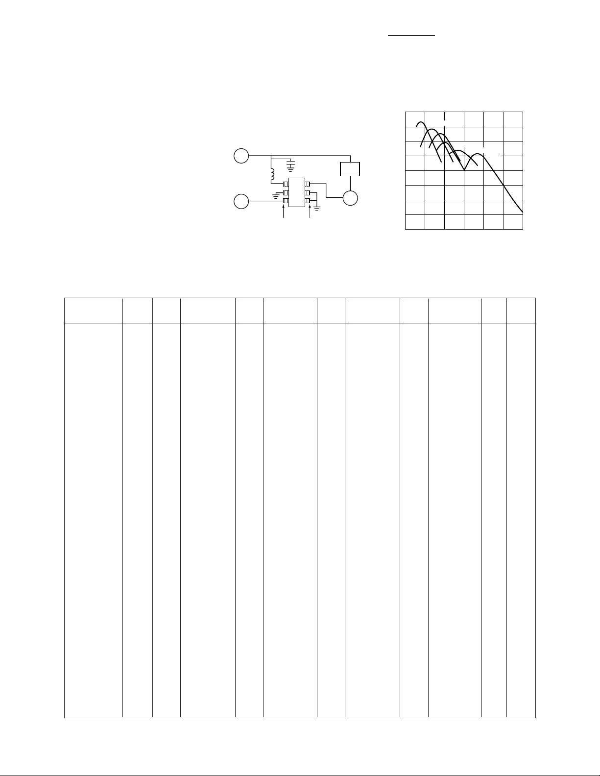
Equivalent Circuit
(Simplified)
• +22 dBm P
3.0 V
+23 dBm P
3.6 V
• 22 dB Small Signal Gain at
2.4 GHz
• Wide Frequency Range 0.5
to 6 GHz
• Single 3 V Supply
• 37% Power Added
Efficiency
• Ultra Miniature Package
d2
Applications
• Amplifier for Driver and
Output Applications
ESD Machine Model (Class A)
ESD Human Body Model (Class 0)
Refer to Agilent Application Note A004R:
Electrostatic Discharge Damage and Control.
V
INPUT
OUTPUT
and V
d1
BIAS
BIAS
d2
GROUND
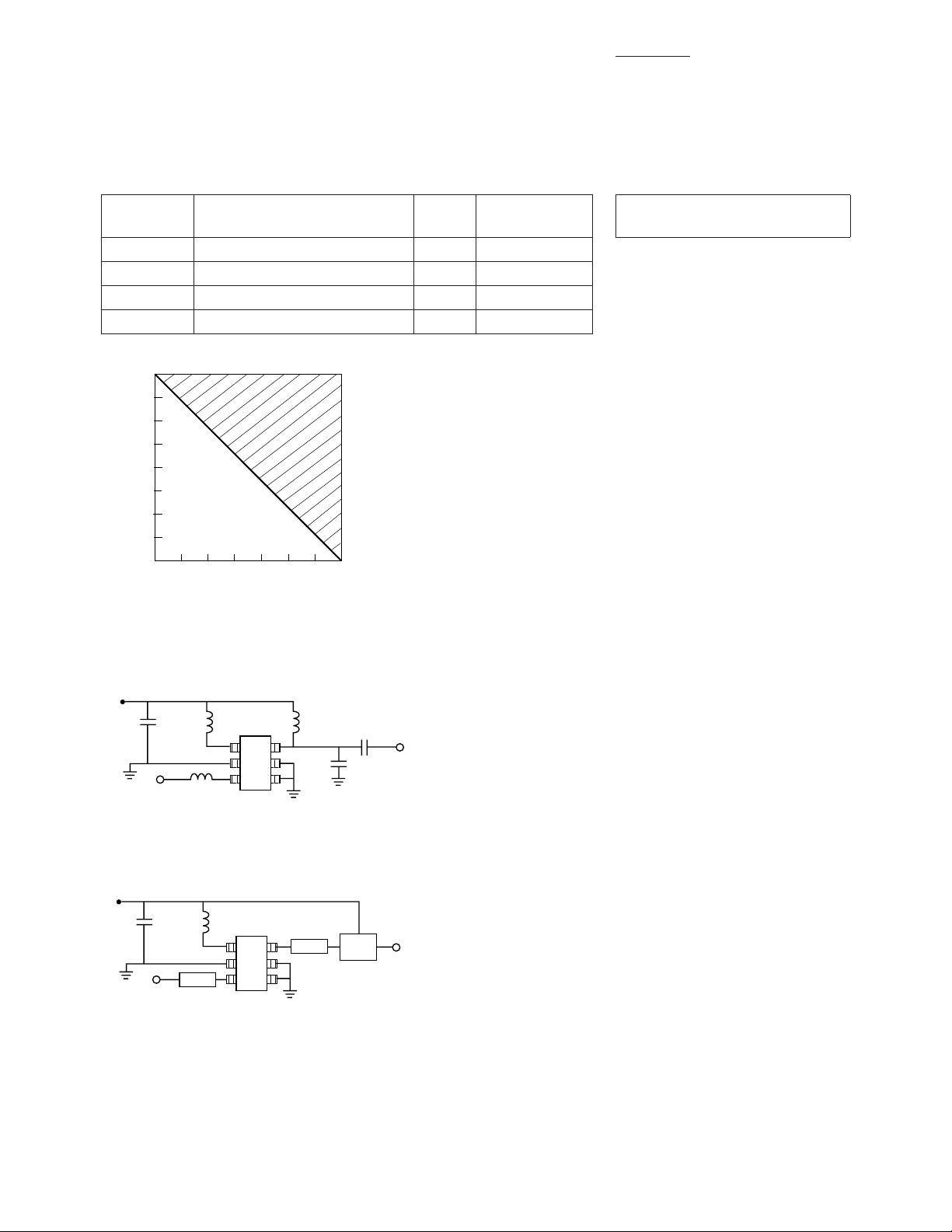
MGA-83563 Absolute Maximum Ratings
Absolute
Symbol Parameter Units Maximum
V Maximum DC Supply Voltage V 4
P
in
T
ch
T
STG
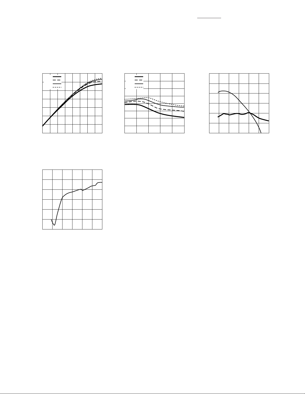
800
700
(mW)
600
500
400
300
200
100
POWER DISSIPATED AS HEAT
Pd = (VOLTAGE) x (CURRENT) – (Pout)
0
10 30 50 70 90 150110
Temperature/ Power Derating Curve.
CW RF Input Power dBm +13
Channel Temperature °C 165
Storage Temperature °C -65 to 150
1 x 10
6
Hrs MTTF
130
CASE TEMPERATURE (°C)
[1]
2
Thermal Resistance
θ
Notes:
1. Operation of this device above any one
of these limits may cause permanent
damage.
= 25°C (TC is defined to be the
2. T
C
temperature at the package pins where
contact is made to the circuit board).
ch to c
= 175°C/W
[2]
:
3.0V
2.2 nH 18 nH20 pF
83
RF
1.2 nH
INPUT
Figure 1. MGA-83563 Final Production Test Circuit.
V
d
L120 pF
83
Tuner
RF
INPUT
Circuit A: L1 = 2.2 nH for 0.1 to 3 GHz
Circuit B: L1 = 0 nH (capacitor as close as possible) for 3 to 6 GHz
Figure 2. MGA-83563 Test Circuit for Characterization.
Tuner
1 pF
50 pF
Bias
Tee
RF
OUTPUT
RF
OUTPUT
3
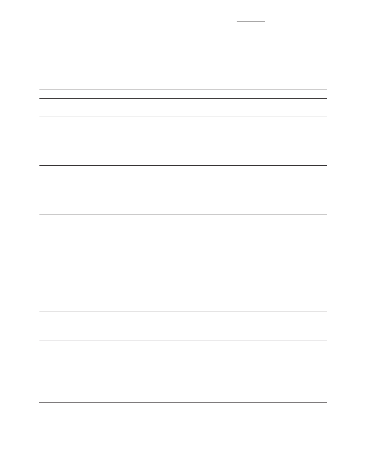
MGA-83563 Electrical Specifications,
Vd = 3 V, TC = 25°C, using test circuit of Figure 2, unless noted.
Std.
Symbol Parameters and Test Conditions Units Min. Typ. Max. Dev.
P
SAT
Saturated Output Power
PAE Power Added Efficiency
I
d
Device Current
[3,5]
[3]
[3]
f = 2.4 GHz dBm 20.5 22.4 0.75
f = 2.4 GHz % 25 37 2.5
mA 152 200 12.4
[4]
Gain Small Signal Gain f = 0.9 GHz dB 20
f = 1.5 GHz 22
f = 2.0 GHz 23
f = 2.4 GHz 22
f = 4.0 GHz 22
f = 5.0 GHz 19
f = 6.0 GHz 17
P
SAT
Saturated Output Power f = 0.9 GHz dBm 20.9
f = 1.5 GHz 21.7
f = 2.0 GHz 21.8
f = 2.4 GHz 22
f = 4.0 GHz 21.9
f = 5.0 GHz 19.7
f = 6.0 GHz 18.2
PAE Power Added Efficiency f = 0.9 GHz % 41
f = 1.5 GHz 41
f = 2.0 GHz 40
f = 2.4 GHz 37
f = 4.0 GHz 32
f = 5.0 GHz 18
f = 6.0 GHz 14
P
1 dB
Output Power at 1 dB Gain Compression
[5]
f = 0.9 GHz dBm 19.1
f = 1.5 GHz 19.7
f = 2.0 GHz 19.7
f = 2.4 GHz 19.2
f = 4.0 GHz 18.1
f = 5.0 GHz 16
f = 6.0 GHz 15
VSWR
Input VSWR into 50 Ω
in
Circuit A f = 0.9 to 1.7 GHz 3.5
= 1.8 to 3.0 GHz 2.6
f
Circuit B f = 3.0 to 6.0 GHz 2.3
VSWR
Output VSWR into 50 Ω
out
Circuit A f = 0.9 to 2.0 GHz 1.4
= 2.0 to 3.0 GHz 2.5
f
Circuit B f = 3.0 to 4.0 GHz 3.5
f = 4.0 to 6.0 GHz 4.5
ISOL Isolation f = 0.9 to 3.0 GHz dB -38
f = 3.0 to 6.0 GHz -30
IP
3
Third Order Intercept Point f = 0.9 GHz to 6.0 GHz dBm 29
Notes:
3. Measured using the final test circuit of Figure 1 with an input power of +4 dBm.
4. Standard Deviation number is based on measurement of at least 500 parts from three non-consecutive wafer lots during
the initial characterization of this product, and is intended to be used as an estimate for distribution of the typical
specification.
5. For linear operation, refer to thermal sections in the Applications section of this data sheet.
4
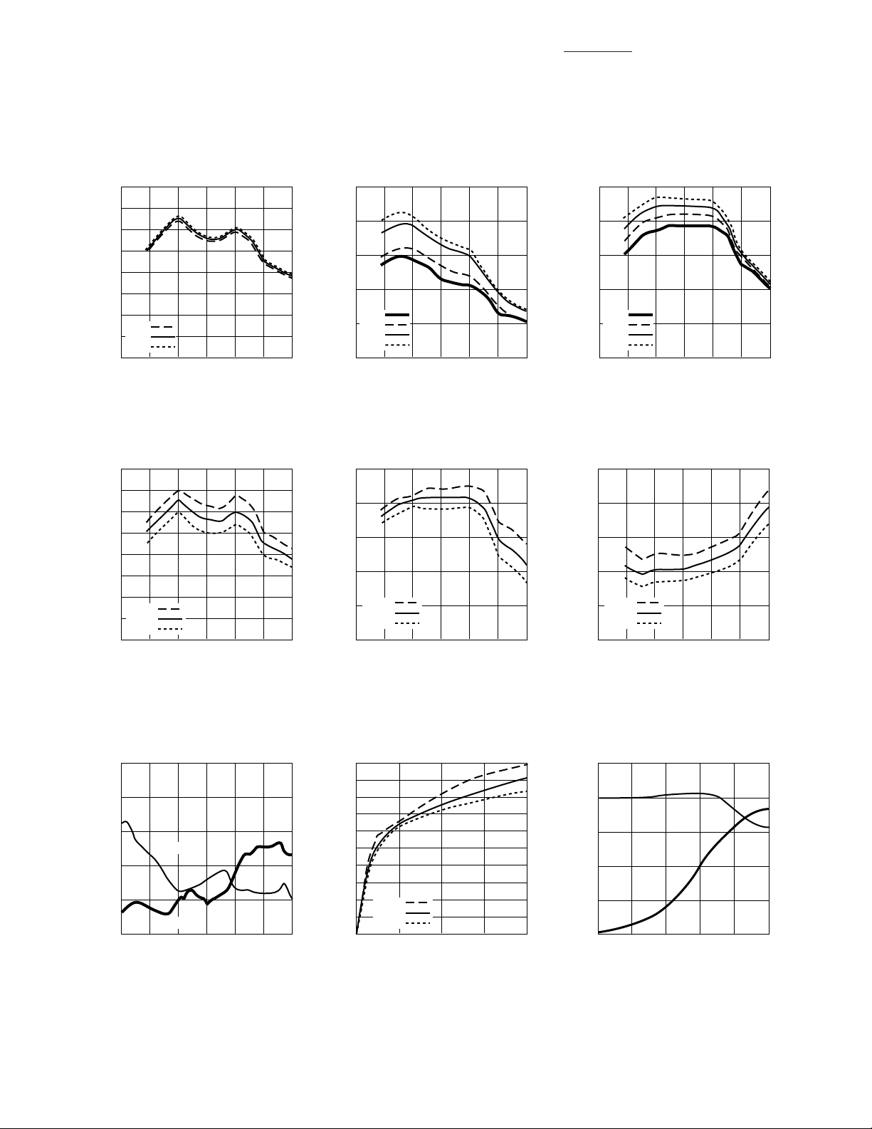
MGA-83563 Typical Performance,
26
24
22
20
(dB)
18
GAIN
16
14
3.3V
12
3.0V
2.7V
10
012 3 4 65
FREQUENCY (GHz)
Figure 3. Tuned Gain vs. Frequency
and Voltage.
26
24
22
20
(dB)
18
GAIN
16
14
-40°C
12
+25°C
+85°C
10
012 3 4 65
FREQUENCY (GHz)
Figure 6. Gain vs. Frequency and
Temperature.
24
22
20
(dBm)
1dB
18
P
2.7V
16
3.0V
3.3V
3.6V
14
012 3 4 65
Figure 4. Output Power at 1 dB
Compression vs. Frequency and Voltage.
24
22
(dBm)
20
18
OUTPUT POWER
16
14
012 3 4 65
Figure 7. Saturated Output Power
(+4 dBm in) vs. Frequency and
Temperature.
Vd = 3 V, TC = 25°C, using test circuit of Figure 2, unless noted.
24
22
20
(dBm)
SAT
18
P
2.7V
16
3.0V
3.3V
3.6V
14
012 3 4 65
FREQUENCY (GHz)
-40°C
+25°C
+85°C
FREQUENCY (GHz)
Figure 5. Saturated Output Power
(+4 dBm in) vs. Frequency and Voltage
12
10
(dB)
8
6
NOISE FIGURE
4
2
012 3 4 65
Figure 8. Noise Figure vs. Frequency
and Temperature.
FREQUENCY (GHz)
-40°C
+25°C
+85°C
FREQUENCY (GHz)
.
10
8
6
VSWR
INPUT
4
2
OUTPUT
0
012 3 4 65
FREQUENCY (GHz)
Figure 9. Input and Output VSWR
vs. Frequency.
200
180
160
(mA)
d
140
120
100
80
60
40
DEVICE CURRENT, I
-40°C
+25°C
20
+85°C
0
012 43
FREQUENCY (GHz)
Figure 10. Supply Current vs. Voltage
and Temperature. Pin = -27 dBm.
190
I
d
170
(mA)
d
150
130
110
DEVICE CURRENT, I
90
-14 -10 -6 -2 2 6
INPUT POWER (dBm) @ 2.4 GHz
PAE
50
40
30
20
10
0
Figure 11. Device Current and Power
Added Efficiency vs. Input Power.
Note: Figure 1 test circuit.
PAE (%)
5
MGA-83563 Typical Performance,
continued
Vd = 3 V, TC = 25°C, using test circuit of Figure 2, unless noted.
24
2.7V
3.0V
22
3.3V
3.6V
20
(dBm)
18
16
14
OUTPUT POWER
12
10
-10 -8 -6 -2
INPUT POWER (dBm) @ 2.4 GHz
-4 2064
Figure 12. Output Power vs. Input
Power and Voltage.
Note: Figure 1 test circuit.
-20
-25
-30
(dB)
-35
33
2.7V
3.0V
32
3.3V
(dBm)
3.6V
31
30
29
28
27
26
THIRD ORDER INTERCEPT
25
-14 -10 -6
INPUT POWER (dBm) @ 2.4 GHz
-2 62
Figure 13. Third Order Intercept
vs. Input Power and Voltage.
Note: Figure 1 test circuit.
50
45
40
(dBm)
3
35
30
PAE (%) and IP
25
20
012 3 4 65
FREQUENCY (GHz)
Figure 14. Power Added Efficiency
and Third Order Intercept vs.
Frequency (V
= 3.6 V).
d
-40
ISOLATION
-45
-50
012 3 4 65
FREQUENCY (GHz)
Figure 15. Isolation vs. Frequency.
6
MGA-83563 Test Circuit
Typical s-parameters are shown
below for various inductor values
(L). Those marked “Sim” are
simulated and those marked
“Meas” are measured using an
frequency before designing an
input, output, or power matching
structure.
V
d
L
50 pF
ICM (Intercontinental Microwave) fixture. Figure 17 shows
IN
the available gain for each L
value. The user should first select
the L value for the application
Figure 16. S-parameter Test Circuit.
s-parameter reference plane
Table 1.
MGA-83563 Typical Scattering Parameters
83
[1]
Bias
Tee
OUT
26
18 nH
24
22
20
(dB)
18
GAIN
16
14
12
10
Figure 17. Available Gain (G
Frequency for the MGA-83563 Amplifier
over Various Inductance Values.
8.2 nH
4.7 nH
2.2 nH
1.2 nH
0 nH
012 3 4 65
FREQUENCY (GHz)
max
TC = 25°C, Vd = 3.0 V, Id = 165 mA, CW Operation, Pin = -27 dBm
Freq. RLin S
11
|S21|2 S
21
Gain S
12
RL
out
S
22
Gmax
L GHz dB Mag Ang Gain Mag Ang dB Mag Ang dB Mag Ang K dB
Sim 18.0 nH 0.6 -4.6 0.59 -48 23.9 15.61 43 -46.7 0.005 105 -21.1 0.09 150 4.47 25.8
Sim 18.0 nH 0.8 -9.6 0.33 -57 24.6 16.96 6 -39.0 0.011 102 -16.8 0.15 -130 2.37 25.2
Sim 18.0 nH 1.0 -16.0 0.16 -27 24.1 16.02 -25 -35.5 0.017 87 -10.1 0.31 -146 1.80 24.6
Sim 18.0 nH 1.4 -10.1 0.31 22 21.7 12.22 -68 -32.8 0.023 66 -5.8 0.51 177 1.48 23.5
Sim 18.0 nH 1.8 -7.3 0.43 17 19.1 9.03 -97 -31.7 0.026 54 -4.4 0.61 150 1.45 22.0
Sim 8.2 nH 0.8 -4.1 0.63 -36 21.2 11.52 48 -47.4 0.004 95 -17.2 0.14 121 6.01 23.5
Sim 8.2 nH 1.0 -5.8 0.51 -45 22.7 13.65 22 -41.1 0.009 111 -35.2 0.02 130 3.13 24.0
Sim 8.2 nH 1.4 -13.0 0.22 -45 23.7 15.30 -27 -33.7 0.021 94 -10.4 0.30 -139 1.54 24.3
Sim 8.2 nH 1.8 -13.0 0.22 13 22.4 13.15 -68 -30.9 0.029 74 -5.5 0.53 -179 1.21 24.1
Sim 8.2 nH 2.0 -10.7 0.29 18 21.3 11.65 -84 -30.3 0.031 67 -4.4 0.60 166 1.16 23.7
Sim 8.2 nH 2.4 -8.2 0.39 15 19.1 8.98 -111 -29.5 0.034 57 -3.4 0.68 141 1.14 22.5
Sim 4.7 nH 1.4 -6.7 0.46 -44 22.1 12.72 4 -37.6 0.013 109 -26.7 0.05 -78 2.44 23.1
Sim 4.7 nH 1.8 -12.0 0.25 -43 22.9 13.99 -37 -32.3 0.024 94 -9.9 0.32 -143 1.44 23.7
Sim 4.7 nH 2.0 -14.3 0.19 -23 22.6 13.53 -57 -30.8 0.029 85 -7.1 0.44 -164 1.26 23.7
Sim 4.7 nH 2.4 -11.9 0.26 10 21.1 11.36 -90 -29.2 0.035 70 -4.3 0.61 163 1.09 23.4
Sim 4.7 nH 2.8 -9.4 0.34 12 19.1 9.03 -115 -28.3 0.038 61 -3.2 0.69 138 1.05 22.5
Meas 2.2 nH 1.8 -6.3 0.49 -53 21.5 11.92 -23 -37.2 0.014 90 -15.1 0.18 -100 2.40 22.8
Meas 2.2 nH 2.0 -7.4 0.43 -51 21.9 12.48 -45 -34.8 0.018 85 -9.7 0.33 -130 1.82 23.3
Meas 2.2 nH 2.4 -7.9 0.40 -36 20.9 11.07 -82 -32.4 0.024 68 -6.2 0.49 -175 1.52 22.8
Meas 2.2 nH 2.8 -7.1 0.44 -27 19.0 8.93 -113 -31.2 0.027 56 -4.1 0.63 150 1.40 22.1
Meas 2.2 nH 3.0 -6.6 0.47 -25 18.0 7.90 -123 -31.0 0.028 52 -4.1 0.62 138 1.48 21.1
Sim 1.2 nH 2.4 -7.9 0.40 -41 20.5 10.61 -36 -33.4 0.021 97 -18.0 0.13 -120 1.98 21.3
Sim 1.2 nH 2.8 -10.8 0.29 -37 20.7 10.90 -67 -30.4 0.030 88 -9.6 0.33 -168 1.47 21.6
Sim 1.2 nH 3.0 -11.9 0.25 -29 20.5 10.56 -82 -29.4 0.034 82 -7.4 0.43 176 1.34 21.6
Sim 1.2 nH 3.2 -12.3 0.24 -20 20.0 9.97 -95 -28.6 0.037 76 -5.9 0.51 161 1.24 21.5
Sim 1.2 nH 3.6 -11.7 0.26 -7 18.6 8.49 -120 -27.5 0.042 67 -4.1 0.62 137 1.14 21.0
Meas 0.0 nH 3.0 -5.6 0.53 -33 17.9 7.87 -13 -39.1 0.011 109 -12.8 0.23 -7 4.07 19.6
Meas 0.0 nH 3.4 -4.7 0.58 -31 20.1 10.13 -43 -34.1 0.020 107 -7.9 0.40 -73 1.72 22.7
Meas 0.0 nH 3.8 -5.5 0.53 -50 20.0 9.95 -81 -31.7 0.026 94 -6.2 0.49 -132 1.43 22.6
Meas 0.0 nH 4.0 -7.4 0.43 -52 19.4 9.28 -94 -30.9 0.028 93 -4.5 0.60 -148 1.38 22.1
Meas 0.0 nH 4.2 -8.4 0.38 -48 18.7 8.62 -106 -30.2 0.031 91 -3.5 0.67 -163 1.27 21.9
Meas 0.0 nH 4.6 -9.0 0.36 -44 17.0 7.08 -129 -28.8 0.036 84 -3.1 0.70 173 1.25 20.5
Meas 0.0 nH 5.0 -9.2 0.35 -39 15.4 5.87 -145 -27.9 0.040 78 -3.0 0.71 155 1.29 19.0
Meas 0.0 nH 5.4 -9.7 0.33 -32 13.8 4.88 -159 -27.2 0.044 77 -3.0 0.71 140 1.38 17.3
Meas 0.0 nH 5.8 -7.8 0.41 -29 12.4 4.16 -170 -25.9 0.051 73 -3.6 0.66 127 1.47 15.7
Meas 0.0 nH 6.0 -6.6 0.47 -46 12.1 4.03 177 -24.9 0.057 64 -3.3 0.68 123 1.33 15.9
Note:
1. Reference plane per Figure 43 in Applications Information section.
) vs.
7
RF
Input
RF
Input
RFC
V
d
3
L2
1
6
MGA-83563 Applications
Information
The MGA-83563 is two-stage,
medium power GaAs RFIC
amplifier designed to be used for
driver and output stages in
MGA-83563 for linear applications
at reduced power levels is
discussed in the “Thermal Design
for Reliability” and “Use of the
MGA-83563 for Linear Applications” in this applications note.
transmitter applications operating
within the 500 MHz to 6 GHz
frequency range.
This device is designed for
operation in the saturated mode
where it delivers a typical output
power of +22 dBm (158 mW) with
a power-added efficiency of 37%.
The MGA-83563 has a large signal
gain of 18 dB requiring an input
signal level of only +4 dBm to
drive it well into saturation. The
high output power and high
efficiency of the MGA-83563,
combined with +3-volt operation
and subminiature packaging,
make this device especially useful
for battery-powered, personal
communication applications such
as wireless data, cellular phones,
and PCS.
The upper end of the frequency
range of the MGA-83563 extends
Application Guidelines
The use of the MGA-83563 is very
straightforward. The on-chip,
partial RF impedance matching
and integrated bias control circuit
simplify the task of using this
device.
The design steps consist of (1)
selecting an interstage inductor
from the data provided, (2)
adding provision for bringing in
the DC bias, and (3) designing
and optimizing an output impedance match for the particular
frequency band of interest. The
input is already well matched to
50 ohms for most frequencies and
in many cases no additional input
matching will be necessary.
Each of the three design steps for
using the MGA-83563 will now be
discussed in greater detail.
Figure 18. Interstage Inductor L2 and
Bias Current.
The values for inductor L2 are
somewhat dependent on the
specific printed circuit board
material, thickness, and RF layout
that are used. The inductor values
shown in Figure 19 have been
created for the PCB and RF
layout that is used for the circuit
examples presented in this
application note. The methodology that was used to determine
the optimum values for L2 and for
creating Figure 19 is presented in
the Appendix. If the user’s PCB
and/or layout differ significantly
from the example circuits, refer
to the Appendix for a description
of how to determine the values of
L2 for any arbitrary frequency,
PCB material, or RF layout.
to 6 GHz making it a useful
solution for medium power
amplifiers in wireless communications products such as 5.7 GHz
spread spectrum or other ISM/
license-free band applications.
Internal capacitors on the RFIC
chip limit the low-end frequency
response to applications above
approximately 500 MHz.
The thermal limitations of the
subminiature SOT-363 (SC-70)
package generally restrict the use
of the MGA-83563 to applications
that use constant envelope types
of modulation. These types of
systems are able to take full
advantage of the MGA-83563’s
high efficiency, saturated mode of
operation. The use of the
Step 1 — Selecting the
Interstage Inductor
The drain of the first stage FET of
this two-stage RFIC amplifier is
connected to package Pin 1. The
supply voltage Vd is connected to
this drain through an inductor,
L2, as shown in Figure 18. The
supply end of the inductor is
bypassed to ground.
This interstage inductor serves
the purpose of completing the
impedance match between the
first and second stages. The value
of inductor L2 depends on the
particular frequency for which
the MGA-83563 is to be used and
is chosen from the look-up graph
in Figure 19.
Step 2 — Bias Connections
The MGA-83563 is a voltage-
biased device and operates from
a single, positive power supply.
The supply voltage, typically
+3-volts, must be applied to the
drains of both stages of the RFIC
amplifier. The connection to the
first stage drain is made through
the interstage inductor, L2, as
described in the previous step.
The supply voltage is applied to
the second stage drain through
Pin 6, which is also the RF Output
connection. Referring to
Figure 18, an inductor (RFC) is
used to separate the RF output
signal from the DC supply. The

8
)
40
30
20
10
9
8
7
6
5
4
L2 (nH)
3
2
1
0.9
0.8
0.7
0.5 1.0 1.5 2.0 2.5 3.0
FREQUENCY (GHz
Figure 19. Values for Interstage Inductor L2.
supply side of the RFC is capacitively bypassed. A DC blocking
capacitor is used at the output to
isolate the supply voltage from
feedback from the RF output to
the drain of the first stage.
Otherwise, the circuit could
become unstable.
the succeeding stage.
The RF Input (Pin 3) connection
In order to prevent loss of output
power, the value of the RFC is
chosen such that its reactance is
several hundred ohms at the
frequency band of operation. At
higher frequencies, it may be
practical to use a length of high
impedance transmission line
(preferably λ/4) in place of the
RFC.
The value of the DC blocking and
RF bypass capacitors are chosen
to provide a small reactance
(typically < 1Ω) at the lowest
operating frequency.
to the MGA-83563 is at DC ground
potential. The use of a DC
blocking capacitor at the input of
the MGA-83563 is not required
unless a circuit that has a DC
voltage present at its output
precedes the RFIC. Although at
ground potential, the input to the
MGA-83563 should not be used as
a current sink.
Step 3 —
Output Impedance Match
The most interesting aspect of
using the MGA-83563 is arriving
at an optimum, large signal
impedance match at the output. A
Since both stages of the RFIC are
biased from the same voltage
source, particular care should be
taken to ensure that the supply
line between the two is well
bypassed to prevent inadvertent
simple but effective approach is
to begin with a circuit that
provides a small signal impedance match, then empirically
adjust the tuning for optimum
large signal performance.
The starting place is to design a
circuit that matches the small
signal Γml (the reflection coeffi-
cient of the load impedance
required to conjugately match the
output of the MGA-83563) to
50 ohms. The small signal
S-parameter data for designing
the output circuit is taken from
Table 1, using the data corre-
sponding to be nearest value of
interstage inductor that was
chosen in step one.
A RF CAD program such as
Agilent’s Touchstone can be used
to easily calculate Γml. Touch-
stone will interpolate the Table 1
S-parameter data for the particu-
lar design frequency of interest.
As the MGA-83563 is driven into
saturation, the output impedance
will generally become lower.
Choose a circuit topology that
will match Γml as well as the
range of impedances on the low
side of Γml. Beginning with this
small signal output match, tune
the circuit under large signal
conditions for maximum
saturated output power and best
efficiency.
It should be noted that both the
saturated output power (P
sat
) and
power-added efficiency (PAE) for
each MGA-83563 is 100% RF
tested at 2.4 GHz in a production
test fixture that simulates an
actual amplifier application. This
method of testing not only
guarantees minimum
performance standards, but also
ensures repeatable RF
performance in the user’s
production circuits.

9
Step 4 (Optional)—
Input Impedance Match
As previously noted, the internal
input impedance match to the
MGA-83563 is already reasonably
good (return loss is typically
8 dB) and may be adequate for
many applications as is. The
design of the MGA-83563 is such
that the second stage will enter
into compression before the first
stage. The isolation provided by
the first stage therefore results in
a minimal impact on the input
matching as the amplifier
becomes saturated.
If an improved input return loss is
needed, an input circuit is designed to match 50 Ω to Γ
ms
(the
reflection coefficient of the
source impedance for a conjugate
match at the input of the
MGA-83563). The value of Γms is
calculated from the S-parameters
in Table 1 in the same way as was
done for Γml. Since the real part
of the input impedance to the
MMIC is near 50 Ω and the
reactive part is capacitive, the
addition of a simple series
inductor is often all that is needed
if a better input match is required.
PCB Layout
Recommendations
When laying out a printed circuit
board for the MGA-83563, several
points should be taken into
account. The PCB layout will be a
balance of electrical, thermal, and
assembly considerations.
Package Footprint
A recommended printed circuit
board footprint for the miniature
SOT-363 (SC-70) package that is
used by the MGA-83563 is shown
in Figure 20.
This package footprint provides
ample allowance for package
placement by automated assembly equipment without adding
parasitics that could impair the
high frequency performance of
the MGA-83563. (The padprint in
Figure 20 is shown with the
footprint of a SOT-363 package
superimposed on the PCB pads
for reference.)
PCB Materials
FR-4 or G-10 printed circuit board
type of material is a good choice
for most low cost wireless
applications for frequencies
through 3 GHz. Typical singlelayer board thickness is 0.020 to
0.031 inches. Multi-layer boards
generally use a dielectric layer
thickness in the 0.005 to
0.010 inch range.
For higher frequency applications, e.g., 5.8 GHz, circuit boards
made with PTFE/glass dielectric
materials are suggested.
0.026
0.079
0.039
0.018
Dimensions in inches.
Figure 20. Recommended PCB Pad
Layout for Agilent’s SC70 6L/SOT-363
Products.
RF Considerations
Starting with the package padprint
of Figure 20, the nucleus of a PCB
layout is shown in Figure 21. This
layout is a good general purpose
starting point for designs using the
MGA-83563 amplifier.
V
d1
Bypass
RF
Input
83
Figure 21. Basic PCB Layout.
Capacitor
L2
RF
Output
This layout is a microstripline
design (solid groundplane on the
backside of the circuit board)
with a 50 Ω input and output and
provision for inductor L2 with its
bypass capacitor.
Adequate RF grounding is critical
to obtain maximum performance
and to maintain device stability.
All of the ground pins of the RFIC
should be connected to the RF
groundplane on the backside of
the PCB by means of plated
through holes (vias) that are
placed very near the package
terminals. As a minimum, one via
should be located next to each
ground pin to ensure good RF
grounding. It is a good practice to
use multiple vias as in Figure 21
to further minimize ground path
inductance.
While it might be considered an
effective RF practice, it is recommended that the PCB pads for the
ground pins not be connected
together underneath the body of
the package for two reasons. The
first reason is that connecting the
ground pins of multi-stage
amplifiers together can sometimes result in undesirable
feedback between stages. Each
ground pin should have its own
independent path to ground. The
second reason is that PCB traces
hidden under the package cannot
be adequately inspected for
solder quality.

10
Thermal Considerations
The DC power dissipation of the
MGA-83563, which can be on the
order of 0.5 watt, is approaching
the thermal limits of subminiature
packaging such as the SOT-363.
As a result, particular care should
be taken to adequately heatsink
the MGA-83563.
The primary heat path from the
MMIC chip to the system heatsink
is by means of conduction
through the package leads and
ground vias to the groundplane
on the backside of the PCB. As
previously mentioned in the
“PCB Layout” section, the use of
multiple vias near all of the
ground pins is desirable for low
inductance. The use of multiple
vias is also an especially important part of the heatsinking
function.
For heatsinking purposes, a
thinner PCB with more vias,
thicker clad metal, and heavier
plating in the vias all result in
lower thermal resistance and
better heat conduction. Circuit
boards thicker than 0.031 inches
are not recommended for both
thermal and electrical reasons.
The importance of good thermal
design on reliability is discussed
in the next section.
Thermal Design for
Reliability
Good thermal design is an
important consideration in the
reliable use of medium power
devices such as the MGA-83563
because the Mean Time To
Failure (MTTF) of semiconductor
devices is inversely proportional
to the operating temperature.
The following examples show the
thermal prerequisites for using
the MGA-83563 reliably in both
saturated and linear modes.
Saturated Mode Thermal
Example
Less heat is dissipated in the
MGA-83563 when operated in the
saturated mode because a
significant amount of power is
removed from the RFIC as RF
signal power. It is for this reason
that the saturated mode allows
the device to be used reliably at
higher circuit board temperatures
than for full power, linear
applications.
As an illustration of a thermal/
reliability calculation, consider
the case of an MGA-83563 biased
at 3.0 volts for use in a saturated
mode application with a MTTF
reliability goal of 10
(114 years). Reliability calculations will first be presented for
nominal conditions, followed by
the conservative approach of
using worst-case conditions.
The first step is to calculate the
power dissipated by the
MGA-86353 as heat. Power flow
for the MGA-83563 is represented
in Figure 22.
P
DC
P
in
Σ
HEAT
Figure 22. Thermal Representation
of MGA-83563.
Pn = 0
6
hours
P
diss
P
out
From Figure 22,
Pin + PDC = P
where Pin and P
+ P
out
are the RF
out
diss
input and output power, PDC is
the DC input power, and P
diss
is
the power dissipated as heat. For
the saturated mode, P
out
= P
sat
,
and,
P
= Pin + PDC – P
diss
sat
From the table of Electrical
Specifications, the device current
(typical) is 152 mA with a power
supply voltage of 3 volts. Referring to Figure 10, it can be seen
that the current will decrease
approximately 8% at elevated
temperatures. The device DC
power consumption is then:
PDC = 3.0 volts * 152 mA * 0.92
PDC = 420 mW
For a saturated amplifier, the RF
input power level is +4 dBm
(2.51 mW) and the saturated
output power is +22 dBm
(158 mW).
The power dissipated as heat is
then:
P
= 2.51 + 420 – 158 mW
diss
P
= 264 mW
diss
The channel-to-case thermal
resistance (θ
) from the table
ch-c
of Absolute Maximum Ratings is
175°C/watt. Note that the meaning of “case” for packages such as
the SOT-363 is defined as the
interface between the package
pins and the mounting surface,
i.e., at the PCB pads. The temperature rise from the mounting
surface to the MMIC channel is
then calculated as
0.264 watt * 175°C/watt, or 46°C.

[1]
Operating life tests
for the
MGA-83563 have established that
a MTTF of 10
6
hours will be met
for channel temperatures ≤ 150°C.
To achieve the 106 hour MTTF
goal, the circuit to which the
device is mounted (i.e., the case
temperature) should therefore
not exceed 150° – 46°C, or 104°C.
Repeating the reliability calculation using the worst case maximum device current of 200 mA,
the DC power dissipation is
552 mW. Summing the RF input
and output powers, P
diss
is
397 mW which results in a
channel-to-case temperature rise
of 69°C. The maximum case
temperature for the MTTF goal of
106 hours is then 150°– 69°C, or
81°C.
For other MTTF goals, power
dissipation, or operating temperatures, Agilent publishes reliability
data sheets based on operating
life tests to enable designers to
arrive at a thermal design for
their particular operating environment. For a reliability data sheet
covering the MGA-83563, request
Agilent publication number 59644128E, titled “GaAs MMIC Amplifier Reliability Data.” This reliability data sheet covers the Agilent
family of PHEMT GaAs RFICs.
Linear Amplifier Thermal
Example
If the MGA-83563 is used in a
linear application, the total power
dissipation is significantly higher
than for the saturated mode. The
dissipated power is greater due to
higher device current (not as
efficient as the saturated mode)
and also because no signal power
is being removed.
The maximum power dissipation
for reliable linear operation is
calculated in the same manner as
was done for the saturated
amplifier example. For linear
circuits, the RF input and output
power are negligible and assumed
to be zero. All of the DC power is
thus dissipated as heat. For
purposes of comparison to the
saturated mode example, this
calculation will use the same
MTTF goal of 106 hours and
supply voltage of 3 volts.
Calculations are again made for
both nominal and worst case
conditions.
From the data of Figure 10, the
typical 3-volt, small signal device
current for the MGA-83563 at
elevated temperatures is 156 mA.
The total device power dissipation, P
, is then 3.0 volts
diss
*
156 mA, or 468 mW. The temperature increment from the RFIC
channel to case is 0.468 watt
*
175°C/watt, or 82°C.
Commensurate with the MTTF
goal of 106 hours, the circuit to
which the device is mounted
should therefore not exceed
150°– 82°C, or 68°C.
For the worst case calculation, a
guard band of 40% is added to the
typical current to arrive at a
maximum DC current of 218 mA.
The P
is 655 mW and the
diss
channel-to-case temperature rise
is 115°C. The maximum case
temperature for worst case
current condition is 35°C.
A case temperature of 68°C for
nominal operation, or 35°C in the
worst case, is unacceptably low
for most applications. In order to
use the MGA-83562 reliably for
linear applications, the P
diss
must
be lowered by reducing the
supply voltage.
11
The implication on RF output
power performance for amplifiers
operating with a reduced Vd is
covered later in this application
note in the section subtitled “Use
of the MGA-83563 for Linear
Applications”.
Design Example for
2.5 GHz
The design of a 2.5 GHz amplifier
will be used to illustrate the
approach for using the
MGA-83563. The basic design
procedure outlined earlier will be
used, in which the interstage
inductor (L2) is chosen first,
followed by the design of an
initial small signal, output match.
The output match will then be
empirically optimized for large
signal conditions after which an
input match will be added.
The printed circuit layout in
Figure 21 is used as the starting
place. The circuit is designed for
fabrication on 0.031-inch thick
FR-4 dielectric material.
Interstage Inductor L2
The first step is to choose a value
for the interstage inductor, L2.
Referring to Figure 19, a value of
1.5 nH corresponds to the design
frequency of 2.5 GHz. A chip
inductor is chosen for L2 in this
example. However, for small
inductance values such as this,
the interstage inductor could also
be realized with a length of high
impedance transmission line.
The interstage inductor is bypassed with a 62 pF capacitor,
which has a reactance of 1 Ω at
2.5 GHz. Connecting the supply
voltage to the bypassed side of
the inductor completes the
interstage part of the amplifier.

12
Output Match
The design of the small signal
output matching circuit begins
with the calculation of the small
signal match impedance, Γml. The
set of S-parameters in Table 1 for
an inductor value of 1.2 nH is
used since this is the closest
value to the 1.5 nH that was
chosen for L2 in the first design
step.
Agilent’s Touchstone program
was used to interpolate the sparameter data and calculate a
Γml of 0.14 ∠172° for 2.5 GHz.
This Γml point is plotted on the
Smith chart in Figure 23 as
Point C, along with an indication
of the area of lower impedance
from this point. (The output
impedance is expected to
decrease under large signal
conditions.) A two-element
matching network consisting of a
shunt capacitor and series
transmission line is chosen to
match the output to 50 ohms.
1
0.5
MLIN
C
B
A
B
-1
C (Γml)
0.2
LARGE SIGNAL
-0.2
Figure 23. Initial Output Match for
Small Signal.
-0.5
RF
Output
The shunt-C, series-line topology
is chosen based on its ability to
cover the expected range of
impedance to be matched and
because it will pass DC bias into
the output pin of the MGA-83563.
A
(50 Ω)
C
21
2
-2
(For the latter reason, impedance
matching circuits using series
capacitors are avoided.)
In some cases, it may be more
practical to implement the series
transmission line element with a
chip inductor. If the series line is
excessively long, the cost of an
additional chip component can be
traded off against circuit board
space. The substitution of an
open-circuit line for the shunt C
may also be possible, thus
eliminating the a capacitor.
Referring to the Smith chart in
Figure 23, the initial output match
for Γml was determined to be a
0.4 pF shunt capacitor followed
by a 0.32-inch length of 50 Ω
microstripline.
DC Bias
A 22 nH RFC is added to the 50 Ω
side of the output matching
circuit to apply bias voltage to the
drain of the second stage. The
RFC is bypassed with a 62 pF
capacitor. A series DC blocking
capacitor, also 62 pF, is added to
the RF output to complete the
bias circuit.
Optimizing the Output
Match
To reach the final output
matching circuit for maximum
saturated output power, an input
power of +4 dBm is applied to
saturate the amplifier circuit. The
output matching circuit is then
experimentally optimized by
adjusting the value of the shunt
capacitor and the distance the
capacitor is located along the
output line from the MGA-83563.
During the tuning process, the
saturated output power of the
amplifier is monitored with a
power meter connected to the
amplifier’s output. An ammeter is
used to observe total device DC
current drain (Id) as an indication
of amplifier efficiency. The
desired output match is then
achieved at the tuning point of
maximum P
and minimum Id.
sat
The optimum output match for
2.5 GHz was achieved with a
shunt capacitor value of 0.9 pF
located 0.08 inches along the 50 Ω
line from the output pin of the
MGA-83563. The final output
circuit is shown in Figure 24.
RF
Input
MGA83563
Figure 24. Final RF Output Match for
the 2.5 GHz Amplifier Tuned for
Maximum P
sat
50 Ω
0.08 in.
.
Output
0.9 pF
RF
When tuned for maximum
saturated output power, the small
signal output return loss for the
amplifier was measured as 5.5 dB
at 2.5 GHz.
Input Match
The input return loss without any
external matching was measured
as 7.6 dB (2.4:1 VWSR). For many
applications no further matching
is necessary. If, however, an
improved input match is required,
a simple series inductor is all that
will be needed.
Agilent’s Touchstone CAD program is again used to extrapolate
the 2.5 GHz S-parameters in Table
1 and calculate a small signal Γ
of 0.37 ∠47°. The conjugate of
Γms, 0.37 ∠-47°, is plotted on the
Smith chart as Point A in
Figure 25.
ms

13
1
0.5
C (50 Ω)
0.2
-0.2
Figure 25. Initial Small Signal Input
Match.
0.2
-0.5
RF
Input
0.5
B
L1
MLIN
1
C
B
-1
A (Γ
2
A
2
*)
ms
-2
The addition of a 0.15 inch length
(actual length on FR-4) of 50 Ω
transmission line rotates Point A
around to Point B on the R = 1
circle of the Smith chart. A series
2.5 nH inductor (L1) is then all
that is required to complete the
match to 50 Ω at Point C.
While the input impedance of the
MGA-83563 is somewhat isolated
from the nonlinear effects of the
saturated output stage, some
empirical optimization of the
input inductor may increase the
input return loss still further. The
input is easily fine-tuned under
large signal conditions by observing the input return loss while an
input power of +4 dBm is applied
to the amplifier. The input
inductor is then “swept” by
placing various values of chip
inductors across the gap provided
in the 50 Ω line at the input of the
MGA-83563. For this example
amplifier, increasing the inductor
from the initial small signal value
of 2.5 nH to 2.7 nH was found to
provide the best input match. The
final input circuit tuned as for
large signal conditions is shown
in Figure 26.
RF
2.7 nH
Input
50 Ω
0.17 in.
Figure 26. Final Large Signal RF Input
Match for the 2.5 GHz Amplifier.
MGA83563
RF
Output
The addition of the 2.7 nH series
inductor increased the large
signal input return loss from
7.6 dB (with no matching) to
14.8 dB (1.4:1 VSWR) at 2.5 GHz.
Completed 2.5 GHz
Amplifier
A schematic diagram of the final
2.5 GHz circuit is shown in
Figure 27. All unmarked capacitors are 62 pF.
V
RF
Output
RFC
Output
d
L1 = 2.7 nH
50 Ω
RF
0.17 in
Input
Figure 27. Schematic Diagram of
2.5 GHz Amplifier.
3
L2 = 1.5 nH
1
83
RFC =
6
50 Ω
0.08 in
22 nH
C2 = 0.9 pF
The completed 2.5 GHz amplifier
assembly with all components is
shown in Figure 28.
+3V
L2
C
C
Input
Figure 28. Completed 2.5 GHz
Amplifier Assembly.
L1
83
CC2
The small signal gain of the
completed amplifier was measured as 22.0 dB at 2.5 GHz. Gain
over a frequency range of 2.0 to
3.0 GHz is shown in Figure 29.
28
26
24
22
(dB)
20
GAIN
18
16
14
2 2.2 2.4 2.6 32.8
FREQUENCY (GHz)
Figure 29. Small Signal Gain of the
Completed 2.5 GHz Amplifier.
The (small signal) input and
output return losses for the
completed amplifier are 14.9 dB
and 5.5 dB respectively at
2.5 GHz. Input and output return
loss over the 2.0 to 3.0 GHz
frequency range is shown in
Figure 30.
0
-5
(dB)
-10
-15
RETURN LOSS
-20
-25
2 2.2 2.4 2.6 32.8
Figure 30. Input and Output
Return Loss of the Completed
2.5 GHz Amplifier.
OUTPUT
INPUT
FREQUENCY (GHz)
Table 2 summarizes measured
results for this particular amplifier at 2.5 GHz.
Output
Mode Gain Power I
(dB) (dBm) (mA)
Small Signal 22.0 — 148
G
-1dB
21.0 19.2 165
Saturated 17.8 21.8 139
Table 2. Performance Summary for
2.5 GHz Amplifier.
d

14
The power-added efficiency
(PAE) in the saturated mode is
36% as calculated from:
P
PAE =
PAE =
Σ
P
(P
P
RF
DC
out – Pin
DC
)
Note the current increases
slightly from small signal conditions to the 1 dB compression
point, then falls appreciably as
the amplifier goes into saturation.
(The 1-dB compressed output
power will be higher for amplifiers that are tuned for linear
performance.)
P
and PAE Sensitivity to
sat
Inductor L2
The output match of the completed 2.5 GHz amplifier was held
fixed while various values of L2
were substituted for the purposes
of (1) verifying the optimum
value for L2, and (2) determining
the sensitivity of P
the value of L2. These results are
plotted in Figure 31.
and PAE to
sat
The length of the series line
between the output of the
MGA-83563 and C2 is also part of
the matching circuit. This line was
not considered as a variable in the
sensitivity analysis since photofabrication of micro-striplines on
circuit boards is highly repeatable.
The most important observation
of this data is that the PAE
remains high for values of C2 that
are toward the left of the maximum P
point (lower values of
sat
C2), while the PAE begins to drop
off toward for higher values of
C2. This data points out the
importance of choosing a value
P
and PAE for each value of C2
sat
are plotted in Figure 32.
Inspection of Figure 32 reveals
that a variation in C2 of ±10% is
acceptable for most applications.
25
20
15
(dBm)
sat
P
10
5
0
0 0.5 1 1.5 42 2.5 3 3.5
for C2 that is toward the lower
side of the maximum P
(lower C2) in order to maintain
high efficiency with production
tolerance components.
P
sat
PAE
L2 (nH)
sat
point
40%
35%
30%
25%
PAE (%)
20%
15%
10%
The data in Figure 31 indicates
there is some tradeoff between
tuning for maximum output
power and maximum efficiency.
The original choice of 1.5 nH for
the interstage inductor L2 appears well optimized.
The results of this tuning process
supplied the 2.5 GHz data point
referred to in the Appendix that
was used to create Plot B of
Figure 47.
Output Match Sensitivity
The sensitivity of P
the value of the shunt capacitor in
the output matching circuit was
investigated by varying the value
of C2 while noting P
current. The input power was
fixed at +4 dBm for this test.
and PAE to
sat
and device
sat
Figure 31. 2.5 GHz P
23
22.5
22
21.5
21
(dBm)
sat
P
20.5
20
19.5
19
18.5
18
0 0.5 1 1.5 2
Figure 32. 2.5 GHz P
and PAE vs. L2.
sat
P
sat
C2 (pF)
and PAE vs. C2.
sat
PAE
50%
45%
40%
35%
30%
25%
20%
15%
10%
(%)
PAE

15
Amplifier Designs for
1.9 GHz and 900 MHz
The same design process used for
the 2.5 GHz amplifier above was
repeated for the design of amplifiers for the 1.9 GHz and 900 MHz
frequency bands. Example
circuits were built using the same
PCB layout as used for the
2.5 GHz amplifier. The schematic
diagram, component values, and
assembly drawing for the 1.9 GHz
and 900 MHz designs are shown
in the “Summary of Example
Amplifiers“ section.
1.9 GHz Amplifier Measured
Results
Performance of this amplifier is
summarized in Table 3. The PAE
is 41%.
Output
Mode Gain Power I
(dB) (dBm) (mA)
Small Signal 23.8 — 155
G
-1dB
22.8 19.6 182
Saturated 17.5 21.5 114
Table 3. Performance Summary for
1.9 GHz Amplifier.
Small signal gain over the 1.5 to
2.3 GHz frequency range is shown
in Figure 33.
26
d
The small signal input and output
return loss over the 1.5 to 2.3 GHz
frequency range is shown in
Figure 34.
0
-4
(dB)
-8
-12
RETURN LOSS
-16
-20
1.5 1.7 1.9 2.1 2.3
Figure 34. Input and Output
Return Loss of the 1.9 GHz
Amplifier.
OUTPUT
INPUT
FREQUENCY (GHz)
900 MHz Amplifier Measured
Results
Measured results for this 900 MHz
amplifier is shown in Table 4. The
PAE is 40%.
Output
Mode Gain Power I
d
(dB) (dBm) (mA)
Small Signal 24.5 — 168
G
-1dB
23.5 20.9 177
Saturated 18.5 22.5 144
Table 4. Performance Summary for
900 MHz Amplifier.
Gain over the 500 to 1300 MHz
frequency range is shown in
Figure 35.
26
24
22
(dB)
20
GAIN
18
16
14
0.5 0.7 0.9 1.1 1.3
FREQUENCY (GHz)
Figure 35. Small Signal Gain of the
900 MHz Amplifier.
Input and output return loss
(small signal) from 500 to
1300 MHz is shown in Figure 36.
0
OUTPUT
-5
(dB)
-10
RETURN LOSS
-15
-20
0.5 0.7 0.9 1.1 1.3
Figure 36. Input and Output
Return Loss of the 900 MHz
Amplifier.
INPUT
FREQUENCY (GHz)
24
22
(dB)
20
GAIN
18
16
14
1.5 1.7 1.9 2.1 2.3
FREQUENCY (GHz)
Figure 33. Small Signal Gain of the
Completed 1.9 GHz Amplifier.

P
and PAE Sensitivity to
sat
Inductor L2 for the 900 MHz
Amplifier
As was done for the 2.5 GHz
amplifier example, values for L2
were “swept” for verification and
to observe sensitivity of P
sat
and
PAE. The results are plotted in
Figure 37. This process verified
the correct value of L2 and
Summary of Example
Amplifiers
A schematic diagram for the three
example amplifiers covering
2.5 GHz, 1.9 GHz, and 900 MHz is
shown in Figure 38.
Component values for the three
designs are summarized in
Table 5.
provided the 900 MHz data point
used in the Appendix to create
Plot B of Figure 47.
23.0
22.8
22.6
22.4
22.2
(dBm)
22.0
sat
P
21.8
21.6
21.4
21.2
21.0
0 5 10 15 454020 25 30 35
P
L2 (nH)
sat
PAE
55%
50%
45%
40%
35%
30%
16
(nH, pF)
900 MHz 1.9 GHz 2.5 GHz
L1 5.6 2.2 2.7
L2 12 2.7 1.5
L3 82 33 22
L4 Not used (short circuit)
C2 3.6 1.2 0.9
C1, C3, C4 150 82 62
C5 1000
Table 5. Component Values for
Example Amplifiers.
Frequency
The completed amplifier with all
components and SMA connectors
is shown in Figure 39. The circuit
is fabricated on 0.031-inch FR-4
material.
The additional 1000 pF bypass
capacitor, C5, was added to the
(%)
bias line near the Vd connection
PAE
to eliminate interstage feedback.
This layout has provision for an
inductor (L4) at the output of the
MGA-83563. This inductor is not
used in for these example amplifiers and is replaced by a short.
Figure 37. 900 MHz P
L1
RF
Input
Figure 38. Schematic Diagram for the Example Amplifiers.
0.17 in
sat
50 Ω
and PAE vs. L2.
C1
L2
3
46
83
1
50 Ω
L4
0.08 in
C4
C2
L3
(RFC)
C3
C5
V
d
RF
Output

17
+V
d
C5
L3
C2
L2
C4
C3
OUT
IN
L1
83
L4
MGA-83-A
Figure 39. Completed MGA-83563 Amplifier Assembly.
Use of the MGA-83563 for
Linear Applications
Due to the thermal limitations
covered in the “Thermal Design
for Reliability” section, the MGA83563 is best suited for use as a
saturated mode amplifier. The
MGA-83563 can however be used
with reduced output power
performance by lowering the
supply voltage.
Some saturated amplifier applications may also benefit from
operation at reduced Vd for the
purpose of reducing current drain
and extending battery life.
P
and P
1dB
2.5 GHz and 900 MHz circuit
examples are shown in Figures 40
and 41, respectively. The methods
presented in the “Thermal Design
for Reliability” section may be
used to arrive at a maximum
supply voltage that corresponds
to the desired MTTF goal.
vs. Vd for the
sat
The P
40 and 41 is taken from the
example amplifiers tuned for
maximum P
higher with linear tuning. When
designing for linear applications,
the value for the interstage
inductor L2 is taken from Plot A
of Figure 47 in the Appendix.
The data in Tables 2–4 shows
that some increase in device
current occurs as the output
power approaches P
ance should be made in the
thermal analysis for the increased
P
diss
or near P
(dBm)
OUTPUT POWER
Figure 40. Output Power vs. Supply Voltage for the 2.5 GHz Amplifier.
power plotted in Figures
1dB
if the circuit is to be used at
1dB
25.00
23.00
21.00
19.00
17.00
15.00
13.00
11.00
9.00
7.00
5.00
1.00 1.25 1.50 1.75 3.00
sat
.
. P
1dB
P
P
will be
. Allow-
1dB
sat
1dB
SUPPLY VOLTAGE, Vd (V)
Operation at Higher
Supply Voltages
While the MGA-83563 is designed
primarily for use in +3 volt
applications, the output power
can be increased by using a
higher supply voltage. Referring
to Figure 5, the P
can be
sat
increased by up to 1 dB by using a
power supply voltage of
+3.6 volts.
Note: If bias voltages greater than
3 volts are used, appropriate
caution should be given to both
the thermal limits and the Absolute Maximum Ratings.
Hints and
Troubleshooting
Oscillation
Unconditional stability of the
MGA-83563 is dependent on
having good grounding. Inadequate device grounding or poor
PCB layout techniques could
cause the device to be potentially
unstable. In a multistage RFIC
such as the MGA-83563, feedback
through bias lines supplying
voltage to both stages can lead to
oscillation. It is important to well
bypass the connections to bias
supply to ensure stable operation.
3.30 3.502.00 2.25 2.50 2.70

18
68%
95%
99%
Parameter Value
Mean (µ)
(typical)
-3σ -2σ -1σ +1σ +2σ +3σ
26.00
24.00
22.00
(dBm)
20.00
18.00
16.00
OUTPUT POWER
14.00
12.00
1.5 3.0 3.52.0 2.5
Figure 41. Output Power vs. Supply Voltage for the 900 MHz Amplifier.
Statistical Parameters
Several categories of parameters
appear within this data sheet.
Parameters may be described
with values that are either
“minimum or maximum,” “typical,” or “standard deviations.”
P
sat
P
1dB
SUPPLY VOLTAGE, Vd (V)
Values for most of the parameters
in the table of Electrical Specifications that are described by
typical data are the mathematical
mean (µ), of the normal distribution taken from the characterization data. For parameters where
measurements or mathematical
The values for parameters are
based on comprehensive product
characterization data, in which
automated measurements are
made on of a minimum of 500
parts taken from three nonconsecutive process lots of
semiconductor wafers. The data
derived from product character-
averaging may not be practical,
such as S-parameters or Noise
Parameters and the performance
curves, the data represents a
nominal part taken from the
center of the characterization
distribution. Typical values are
intended to be used as a basis for
electrical design.
ization tends to be normally
distributed, e.g., fits the standard
bell curve.
To assist designers in optimizing
not only the immediate amplifier
circuit using the MGA-83563, but
Parameters considered to be the
most important to system performance are bounded by minimum
or maximum values. For the
MGA-83563, these parameters
are: Saturated Output Power
(P
), Power Added Efficiency
sat
(PAE), and Device Current (Id).
Each of the guaranteed parameters is 100% tested as part of the
manufacturing process.
to also evaluate and optimize
trade-offs that affect a complete
wireless system, the standard
deviation (σ) is provided for
many of the Electrical Specifica-
tions parameters (at 25°C) in
addition to the mean. The stan-
dard deviation is a measure of the
variability about the mean. It will
be recalled that a normal distribu-
tion is completely described by
the mean and standard deviation.
Standard statistics tables or
calculations provide the probability of a parameter falling between
any two values, usually symmetrically located about the mean.
Referring to Figure 42 for example, the probability of a
parameter being between ±1σ is
68.3%; between ±2σ is 95.4%; and
between ±3σ is 99.7%.
Figure 42. Normal Distribution.
Phase Reference Planes
The positions of the reference
planes used to specify S-parameters and Noise Parameters for
the MGA-83563 are shown in
Figure 43. As seen in the illustration, the reference planes are
located at the point where the
package leads contact the test
circuit.
REFERENCE
PLANES
TEST CIRCUIT
Figure 43. Phase Reference Planes.

19
Appendix —
Determination of
Interstage Inductor
Value.
A methodology is presented here
for determining the value of the
interstage inductor, L2 that
produces optimum large signal
performance at any frequency.
This is the method used to create
the plot of Optimum L2 vs.
Frequency in Figure 19. This
procedure is included as a
reference for PCB designs that
may differ considerably from the
example circuit of Figure 40.
While the method described here
covers a wide range of frequencies for generic applications, the
same approach can be used for a
single frequency of interest.
Although the printed circuit
board layout of Figure 40 is used
here for demonstration purposes,
the same procedure is equally
applicable to the any other circuit
board material, thickness, or
topology.
This is a 2-step process in which
the value for L2 for best small
signal performance is first
ascertained followed by an
empirical adjustment of L2 to
allow for large signal effects.
The first step in this process is to
assemble a test circuit for the
MGA-83563 with 50-ohm input
and output lines. This test circuit
should use the same printed
circuit board material, thickness,
and ground via arrangement for
the MGA-83563 that will be used
to the final amplifier circuit. The
connection to Pin 1 should have
provision for a chip inductor that
is bypassed to ground. The
bypassed side of the inductor is
connected to the supply voltage.
The supply voltage is also con-
nected to the RF Output/V
d2
(Pin 6) by means of an external,
wideband bias tee. The test
circuit is shown in Figure 44.
BIAS
TEE
+V
OUT
Test Circuit
L2
IN
Figure 44. L2 Test Circuit.
MGA83563
50 Ω50 Ω
Next, the wideband gain response
of the test circuit is observed
while substituting various values
of chip inductors for L2. For each
value of L2, the gain should be
plotted and/or the frequency at
which the maximum gain occurs
recorded. Note that the small
signal input and output match
provided by the internal matching
of the MGA-83563 is sufficiently
close to 50 ohms for most combi-
nations of L2 and frequencies that
further matching would not
significantly skew the data. This
is a small signal test and the input
power level should be less than
-15 dBm.
25
20
15
(dB)
10
GAIN
5
0
0.5 1.0 2.0
FREQUENCY (GHz)
Figure 45. Small Signal Gain vs.
Frequency for Various Values of L2.
6.8
15
33
4.0
Various values of Toko, Inc.
4.7
0 nH
1.5
2.7
5.03.0 6.0
©
type LL1608 inductors were used
for this particular example. An
inductance value of 0.5 nH was
used for the case of a short
circuit placed across the gap
provided for L2. For use at
5.8 GHz, Pin 1 should be bypassed
through the most direct path
(minimum inductance) to ground.
d
Referring to Figure 21, L2 is not
used and a bypass capacitor is
placed from Pin 1 directly to the
ground pad for Pin 2.
The result of this step is the
multiple plot shown in Figure 45
of gain vs. frequency with L2 as a
parameter. This plot is similar to
the plot in Table 1, but differs in
that the data in Figure 45 is
specific to the designer’s particular PCB layout. The Table 1 data
is a combination of test data
taken in a relatively parasiticsterile characterization fixture
and computer simulations. The
test data in Figure 45 includes the
effects of all circuit parasitics,
ground vias, parasitics of the
actual chip inductor that will be
used, and also takes into account
the length of line and bypass
capacitor used to make the
connection to L2 that will be used
in the final circuit.
The value of L2 is then plotted vs.
the frequency at which the gain
peak occurred for each value of
inductance. This plot is done as a
log plot with a straight-line curve
fit added to smooth the data. This
data, shown as Plot A in Figure
46, then gives the optimum value
of L2 for maximum small signal
gain, i.e., linear performance.
The results of the 2.5 GHz and
900 MHz example amplifiers
presented in this Application
Note were used to modify Plot A
for large signal use. The optimum,
large signal value for L2 at
2.5 GHz was determined to be

20
1.5 nH, and 12 nH for 900 MHz.
These two L2-frequency points
are added to the data plot of
Figure 46. A straight line is drawn
through these two points to
create Plot B.
Plot B provides a look-up for
values of L2 for saturated amplifier designs. Plot A is used for
linear amplifiers. Note: Plot B is
replicated as Figure 19 in the
“Application Guidelines” section
of this note.
[1]
Operating life test conducted for a case
temperature of 60°C and with a Vd of
3.6 volts. After 1000 hours, there were 0
failures.
40
30
20
10
9
8
7
6
5
4
L2 (nH)
3
2
1
0.9
0.8
0.7
0.5 1.0 1.5 2.0 2.5 3.0
PLOT A
PLOT B
FREQUENCY (GHz)
Figure 46. Optimum L2 for Small Signal Gain vs. Frequency.

Package Dimensions
Outline 63 (SOT-363/SC-70)
21
HE
A1
SYMBOL
E
D
HE
A
A2
A1
Q1
e
b
c
L
e
b
DIMENSIONS (mm)
MIN.
1.15
1.80
1.80
0.80
0.80
0.00
0.10
0.650 BCS
0.15
0.10
0.10
D
MAX.
1.35
2.25
2.40
1.10
1.00
0.10
0.40
0.30
0.20
0.30
E
Q1
A2
A
L
NOTES:
1. All dimensions are in mm.
2. Dimensions are inclusive of plating.
3. Dimensions are exclusive of mold flash & metal burr.
4. All specifications comply to EIAJ SC70.
5. Die is facing up for mold and facing down for trim/form,
ie: reverse trim/form.
6. Package surface to be mirror finish.
c
Part Number Ordering Information
No. of
Part Number Devices Container
MGA-83563-TR1 3000 7" Reel
MGA-83563-TR2 10000 13" Reel
MGA-83563-BLK 100 antistatic bag
MGA-83563-TR1G 3000 7" Reel
MGA-83563-TR2G 10000 13" Reel
MGA-83563-BLKG 100 antistatic bag
Note: For lead-free option, the part number will have the
character “G” at the end.

Device Orientation
REEL
TOP VIEW
4 mm
END VIEW
CARRIER
8 mm
TAPE
USER
FEED
DIRECTION
COVER TAPE
Tape Dimensions and Product Orientation
For Outline 63
P
P
0
C
t
(CARRIER TAPE THICKNESS) Tt (COVER TAPE THICKNESS)
1
10° MAX.
D
D
1
K
0
83x 83x 83x 83x
P
2
10° MAX.
E
F
W
A
0
CAVITY
PERFORATION
CARRIER TAPE
COVER TAPE
DISTANCE
For product information and a complete list of Agilent
contacts and distributors, please go to our web site.
DESCRIPTION SYMBOL SIZE (mm) SIZE (INCHES)
LENGTH
WIDTH
DEPTH
PITCH
BOTTOM HOLE DIAMETER
DIAMETER
PITCH
POSITION
WIDTH
THICKNESS
WIDTH
TAPE THICKNESS
CAVITY TO PERFORATION
(WIDTH DIRECTION)
CAVITY TO PERFORATION
(LENGTH DIRECTION)
A
0
B
0
K
0
P
D
1
D
P
0
E
W
t
1
C
T
t
F
P
2
www.agilent.com/semiconductors
E-mail: SemiconductorSupport@agilent.com
Data subject to change.
Copyright © 2004-2005 Agilent Technologies, Inc.
Obsoletes 5989-1800EN
November 3, 2005
5989-4188EN
2.40 ± 0.10
2.40 ± 0.10
1.20 ± 0.10
4.00 ± 0.10
1.00 + 0.25
1.55 ± 0.10
4.00 ± 0.10
1.75 ± 0.10
8.00 + 0.30 - 0.10
0.254 ± 0.02
5.40 ± 0.10
0.062 ± 0.001
3.50 ± 0.05
2.00 ± 0.05
0.094 ± 0.004
0.094 ± 0.004
0.047 ± 0.004
0.157 ± 0.004
0.039 + 0.010
0.061 + 0.002
0.157 ± 0.004
0.069 ± 0.004
0.315 + 0.012
0.0100 ± 0.0008
0.205 + 0.004
0.0025 ± 0.0004
0.138 ± 0.002
0.079 ± 0.002
B
0
 Loading...